Three-dimensional electrical control of the excitonic fine structure for a quantum dot in a cavity
Abstract
The excitonic fine structure plays a key role for the quantum light generated by semiconductor quantum dots, both for entangled photon pairs and single photons. Controlling the excitonic fine structure has been demonstrated using electric, magnetic, or strain fields, but not for quantum dots in optical cavities, a key requirement to obtain high source efficiency and near-unity photon indistinguishability. Here, we demonstrate the control of the fine structure splitting for quantum dots embedded in micropillar cavities. We propose a scheme based on remote electrical contacts connected to the pillar cavity through narrow ridges. Numerical simulations show that such a geometry allows for a three-dimensional control of the electrical field. We experimentally demonstrate tuning and reproducible canceling of the fine structure, a crucial step for the reproducibility of quantum light source technology.
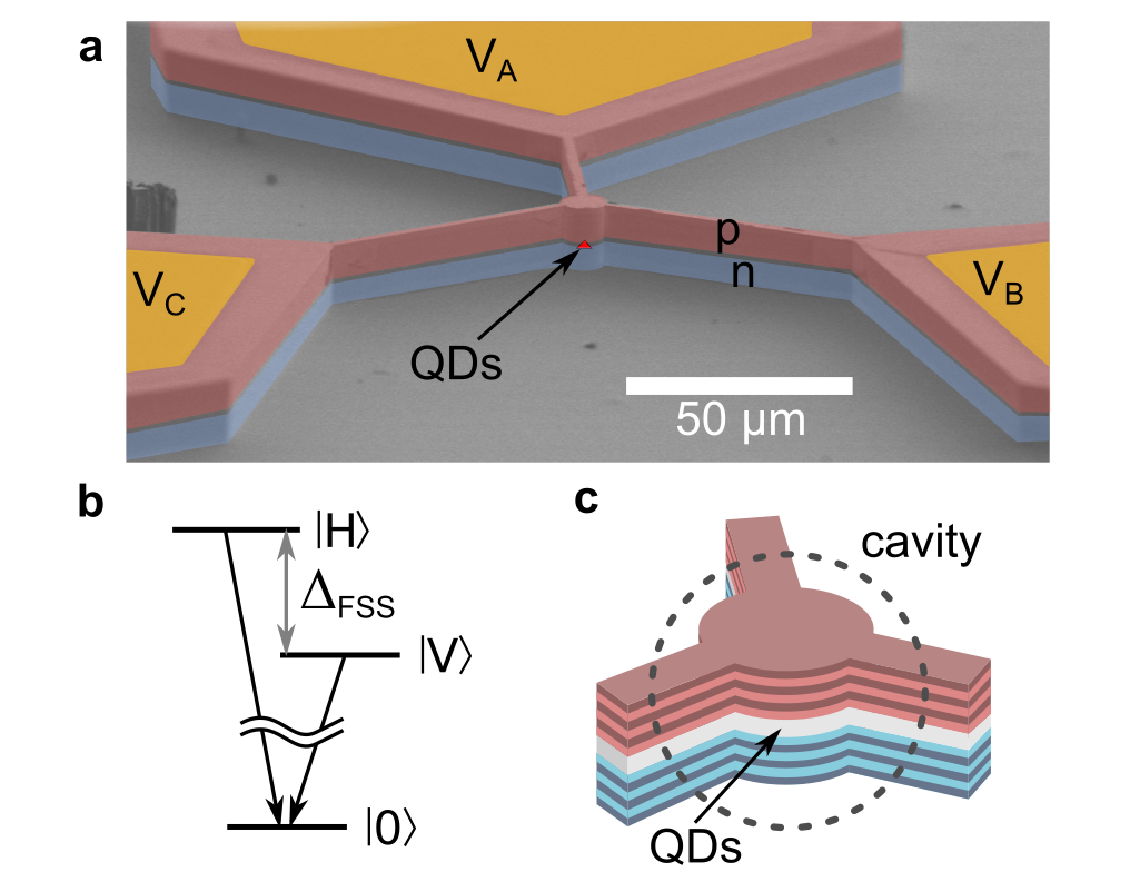
Semiconductor quantum dots (QDs) have emerged as excellent emitters of single photons Senellart et al. (2017) and entangled photon pairs Schimpf et al. (2021); Jöns et al. (2017) with exciting prospects for both optical quantum networks and processors. The neutral exciton state in an epitaxially grown QD exhibits a fine structure splitting (FSS) arising from a reduced symmetry of the nanostructure as well as valence band mixing (see Fig. 1(b)) Bayer et al. (2002); Léger et al. (2007). Cancelling this FSS has long been identified as a key requirement for the on-demand generation of polarization-entangled photon pairs via the radiative biexciton-exciton cascade Benson et al. (2000); Liu et al. (2019). Similarly, near-zero FSS was shown to enable high fidelity initialization of long-lived quantum dot hole spin qubits Brash et al. (2015). Conversely, it was very recently shown that the brightness of an exciton based single-photon source under resonant pumping could be optimized for an optimal finite FSS value Ollivier et al. (2020). All these perspectives have led to the development of a large variety of techniques to control the FSS. Material growth and processing are tailored to reduce the average FSS, for instance growing small QDs Stevenson et al. (2006), performing post growth annealing Young et al. (2005) or using droplet epitaxy Huo et al. (2013). Fine tuning of the residual FSS was explored through the application of both magnetic and electric fields Kowalik et al. (2005); Gerardot et al. (2007); Stevenson et al. (2006) as well as strain Seidl et al. (2006); Kuklewicz et al. (2012).
However, the control of a single degree of freedom only leads to zero FSS if the applied field points along the major axis of QD asymmetry Gong et al. (2011); Plumhof et al. (2011); Bennett et al. (2010). To universally eliminate the FSS, it was theoretically shown that two independent and non-parallel external controls are needed Trotta et al. (2012), e.g. biaxial strain or two vector components of an applied electromagnetic field.
Adding a third control further allows independent tuning of the FSS and the average exciton transition energy Trotta et al. (2015).
Over the years, the toolbox for controlling the excitonic fine structure has become quite diverse and efficient, leading to record entanglement fidelity for entangled photon pairs Huber et al. (2018). However, such control has not yet been achieved for QDs inserted in optical cavities, a crucial step to ensure high collection efficiency of the single and entangled photonsWang et al. (2016); Somaschi et al. (2016); Dousse et al. (2010), and for reaching near unity photon indistinguishability Somaschi et al. (2016); Wang et al. (2016); Tomm et al. (2021).
Here, we propose a structure that allows controlling the excitonic FSS for quantum dots inserted in monolithic micropillar cavities. We define three independent control knobs by remotely applying three electric potentials on large p-i-n diodes that are connected to the pillar cavity through narrow ridges. The vertical p-i-n doping profile extends over the full device. Finite element simulations are conducted to monitor both the stationary electric field and current in the structure for various bias situations, evidencing a control of the electric field at the position of the QD in all three directions of space. We experimentally explore this approach and demonstrate both a control of the FFS amplitude and of the orientation of the exciton transition dipoles. We find that various combinations of applied voltages reduce the FSS close or below the radiative linewidth. Furthermore, similar values of FSS can be obtained for different excitonic wavelengths.
The structure proposed to control the excitonic FSS for a QD in a cavity is illustrated in Fig. 1(a). We start from a planar GaAs/AlGaAs microcavity grown on a GaAs substrate. For the sample under investigation, the bottom (top) distributed Bragg reflector (DBR) consists of 34 (16) pairs of thick GaAs/AlGaAs layers. The DBRs surround a thick GaAs cavity spacer with a layer of annealed InGaAs QDs in its center. Vertically, the multilayer structure defines a p-i-n junction with p(n) doping for the top (bottom) mirror and an intrinsic region within the cavity spacer embedding the QDs. Laterally, the planar structure is etched to define circular pillar cavities with µm diameters that are connected through three µm wide, µm long ridges to large mesas where titanium-gold pads are defined for electrical connection. Each pad can be connected to an independent voltage source with the gold-coated back of the substrate defining a common ground potential. By applying various values for the three biases labelled , and , one can control the amplitude and direction of the electric field at the center of the pillar cavity in the three directions of space.
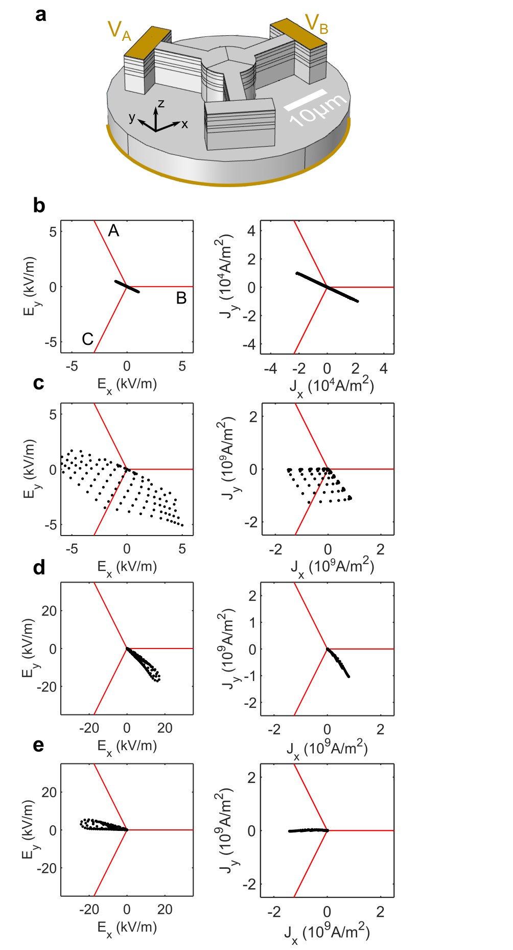
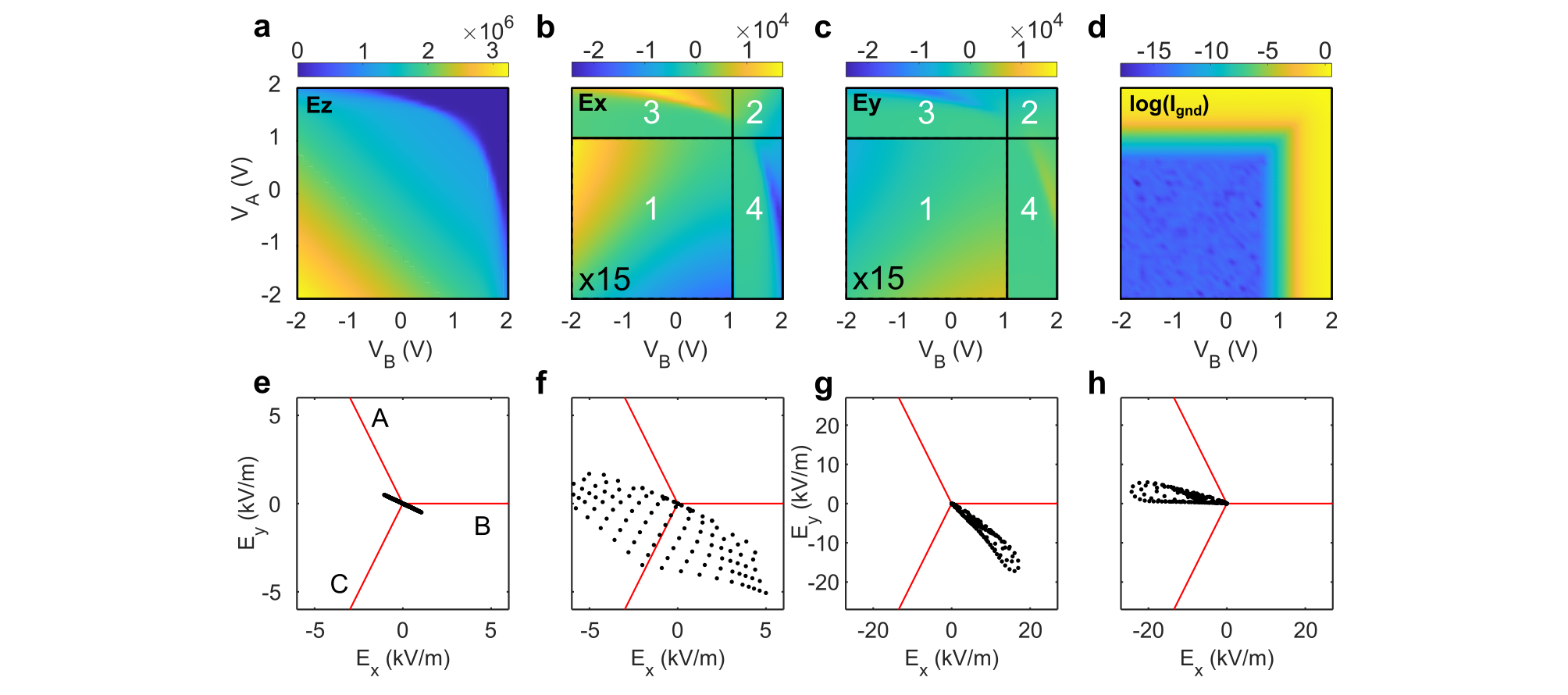
To evidence such a possibility, we first performed Finite Elements Method (FEM) simulations (COMSOL Multiphysics). For computational efficiency, we replaced the vertical DBR layer structure by a single GaAs slab with a vertical p-i-n doping profile. Such a simplification allows for a qualitative understanding of the physics at play disregarding the complex modulation doping structure that one needs to implement in the DBR structure. Figures 2(a-c) display the three electric field components at the center of the micropillar cavity - both in the vertical and horizontal direction - as a function of two applied electric potentials and , while is not fixed by an external potential. Along the vertical direction, the calculated electric field presents a large amplitude for negative values of and , and progressively decreases when going to the passing regime for both diodes A and B. The in-plane electric field components, on the other end, show a more subtle behavior and four regimes can be identified as indicated in the four areas labelled 1 through 4 in Fig 2(b-c). They essentially correspond to the regimes of non-passing and passing p-i-n junction for each of the two electric potentials as evidenced by Fig. 2(d) presenting the total current flowing through the device (in logarithmic scale).
Figures 2(e-h) present the in-plane electric field components in polar plots for each regime. For area 1 (Fig. 2(e)), the amplitude of the field depends on the applied voltage but its direction remains normal to the unconnected ridge C: the current flows along the p-doped upper DBR with an in-plane field parallel to it, dictated by the Ohmic resistivity of the p-doped material. The direction of the in-plane electric field can be modified when the junctions are in the passing regime. This is the case for area 2 (Fig. 2(f)) for which the accessible values of in-plane electric field cover an angular range of almost . Effectively, we generate two independent non-parallel current components which are both drained to the common ground on the back side of the p-i-n junction. Finally, there are two intermediate cases found in areas 3 and 4 of the field maps for which one diode only is in the passing regime. For area 3 (4), the field mostly points in the direction of diode A (B), yet with a noticeable steering effect resulting from the second applied voltage presenting a current drain on the top surface.
Based on the above discussion, we find that there are at least two ways to generate in-plane electric fields with directional control at the position of a QD centered in the micropillar device. First, in the limit of a non-passing p-i-n junction, using the third control knob (in addition to and ) would allow to choose the field amplitude in the three directions that are normal to each one of the ridges as it was the case in the direction normal to ridge C with only one pair of voltages ( and ) in Fig. 2(e). Second, in the limit of large forward bias, two electric potentials suffice to control both orientation and magnitude of the field. The maximum attainable magnitude of the in-plane electric field differs by roughly a factor of four between the regimes.
The link between the observed in-plane electric field behavior and current flows is shown in supplementary figure 2. In all regimes, except for area 2, the current and electric field are roughly parallel. For area 2, two non-parallel current components are created which are both drained through the p-i-n junction in the passing regime. We underline however that the absolute value of the calculated current is largely over-estimated numerically, because of the strongly simplified doping structured considered in the z direction, as experimentally evidenced hereafter.
We tested this FFS control scheme experimentally on 10 µm diameter pillar cavities. Such large diameter cavities do not show discrete optical modes, so that any cavity bi-refringence effect that could perturb the polarization analysis of the excitonic fine structure is avoided Moczała-Dusanowska et al. (2019).
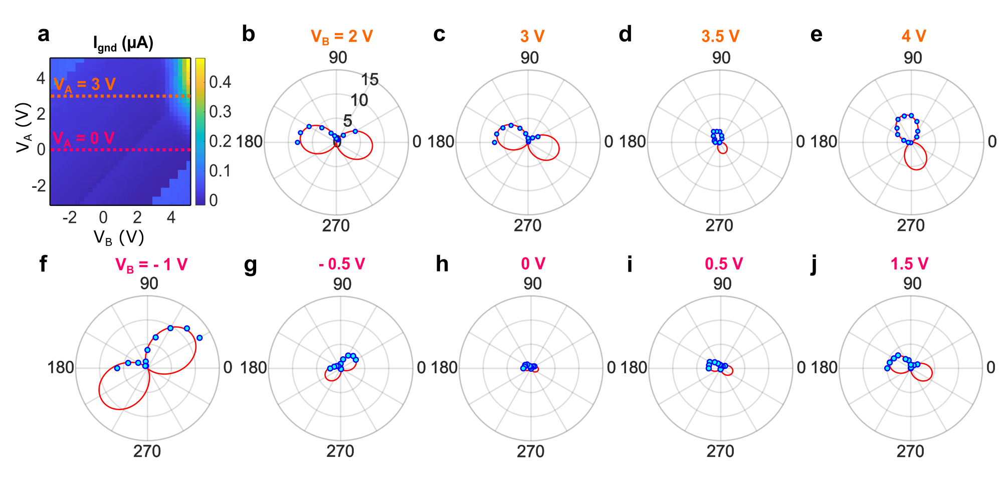
The FSS is optically probed through polarization-resolved micro-photoluminescence (µPL) studies performed at 4K, under quasi-resonant (p-shell) continuous-wave excitation Gazzano et al. (2013). We present experimental data for two QDs (QD1 and QD2) inserted in two distinct cavities. Figure 3 shows the data set obtained for QD1. Figure 3(a) presents the measured sum of currents flowing through the connections to the two independent voltage sources. This sum corresponds the portion of the current that flows through the p-i-n junction, since the horizontal current flowing on top of the device cancels out. Figure 3(a) allows one to identify the various regimes for the FSS control and evidences maximal current in the range, orders of magnitudes lower than predicted by our simplified numerical simulations. The passing regime is obtained for and .
This asymmetry, that is not accounted for in our numerical simulations, can be due to the imperfections of the 1D ridges exhibiting different Ohmic resistances.
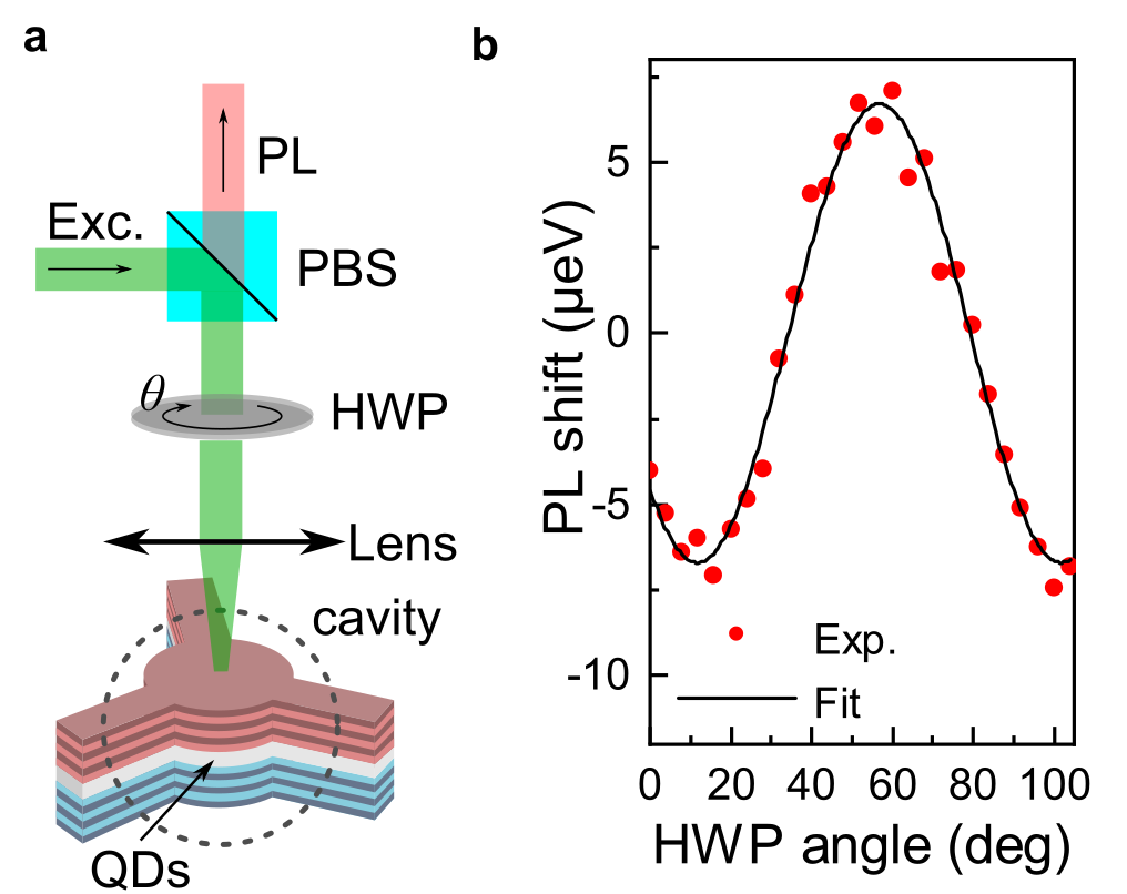
The small FSS of our QDs is not spectrally resolved by our setup, however the exciton photoluminescence peak energy undergoes a clear sinusoidal shift of amplitude in the 10 µeV range as a function of the angle of the detected linear polarization. This measurement is achieved here by rotating a half-wave-plate before a fixed polarizer (See supplementary). In Fig. 3(b-e), polar plots of this shift are reported for different voltages at a fixed voltage V. For each voltage, the angular dependence is fitted by the function where refers to the polarization angle of the high energy exciton line. A reduction of down to µeV is observed at 3.5 V, at the edge of the passing regime, together with a rotation of the exciton eigenaxes on the order of . This is the characteristic signature of near cancellation of the FSS in such a way that the eigenaxes of the high and low energy exciton lines are exchanged when (ideally) crossing the zero FSS point Bennett et al. (2010); Trotta et al. (2012). A further reduction down to µeV is observed at a fixed voltage V (non-passing regime) when varying , as seen in Fig. 3(f-j). For both the passing and non-passing regimes, a significant reduction of the FSS near or below the radiative linewidth is thus demonstrated, whereas over the whole voltage scans, we observed significant variations of FSS amplitude up to µeV.
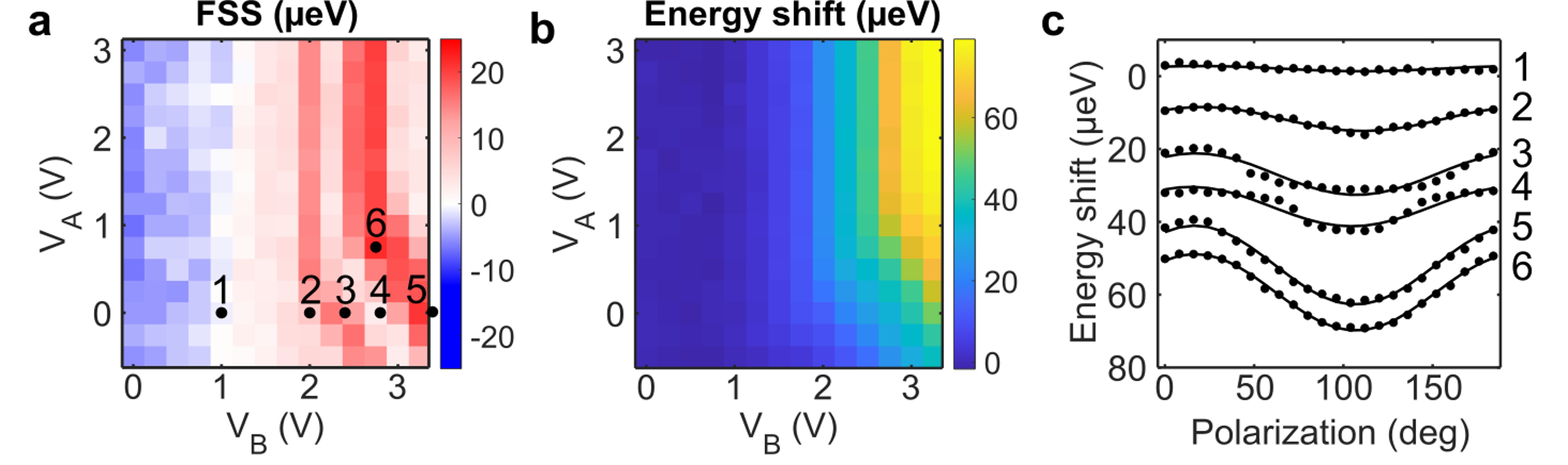
To complete the experimental picture, we report similar results for QD2 in Figure 4. Here, the exciton peak energy is measured for each value of () for the exciton eigenaxes identified for V. We deduce an algebraic value for FSS defined as the energy difference between these two energies. Figure 4(a) shows that the algebraic FSS varies over more than 20 µeV and exhibits a clear transition at the voltage V where the algebraic FSS changes sign. To determine whether it is due to FSS cancellation (and not only to a rotation of the QD eigenaxes Bennett et al. (2010); Trotta et al. (2012)), the exciton peak energy is measured as a function of the angle of detected polarization, for 6 different points as indicated in Fig. 4(a). The sinusoidal dependence reported in Fig. 4(d) does not show any significant rotation of the eigenaxes in the probed region of positive FSS and a vanishing FSS of µeV, below the radiative linewidth for point 1 in Fig. 4(a). Besides, when considering a fixed value of and increasing , the FSS turns out to vary non monotonously, showing notably a local minimum at V, a behavior also observed for QD1. Such an observation is not directly explained by the electrical field which, according to our numerical simulations, should evolve monotonously. This rather reveals the complex dependence of FSS on the electric field, as already reported in Ref. Gerardot et al., 2007 for an in-plane application of an electric field. Combined with the average exciton energy shift due to the quantum confined Stark effect, covering a range around 80 µeV as shown in Fig. 4(b), this behaviour is of particular interest to reduce or modify the FSS for different central exciton energies. Such a possibility is evidenced in Fig. 4(b) where similar FSS values are obtained at different exciton energy for voltage combination 3 and 4 as well as for 5 and 6.
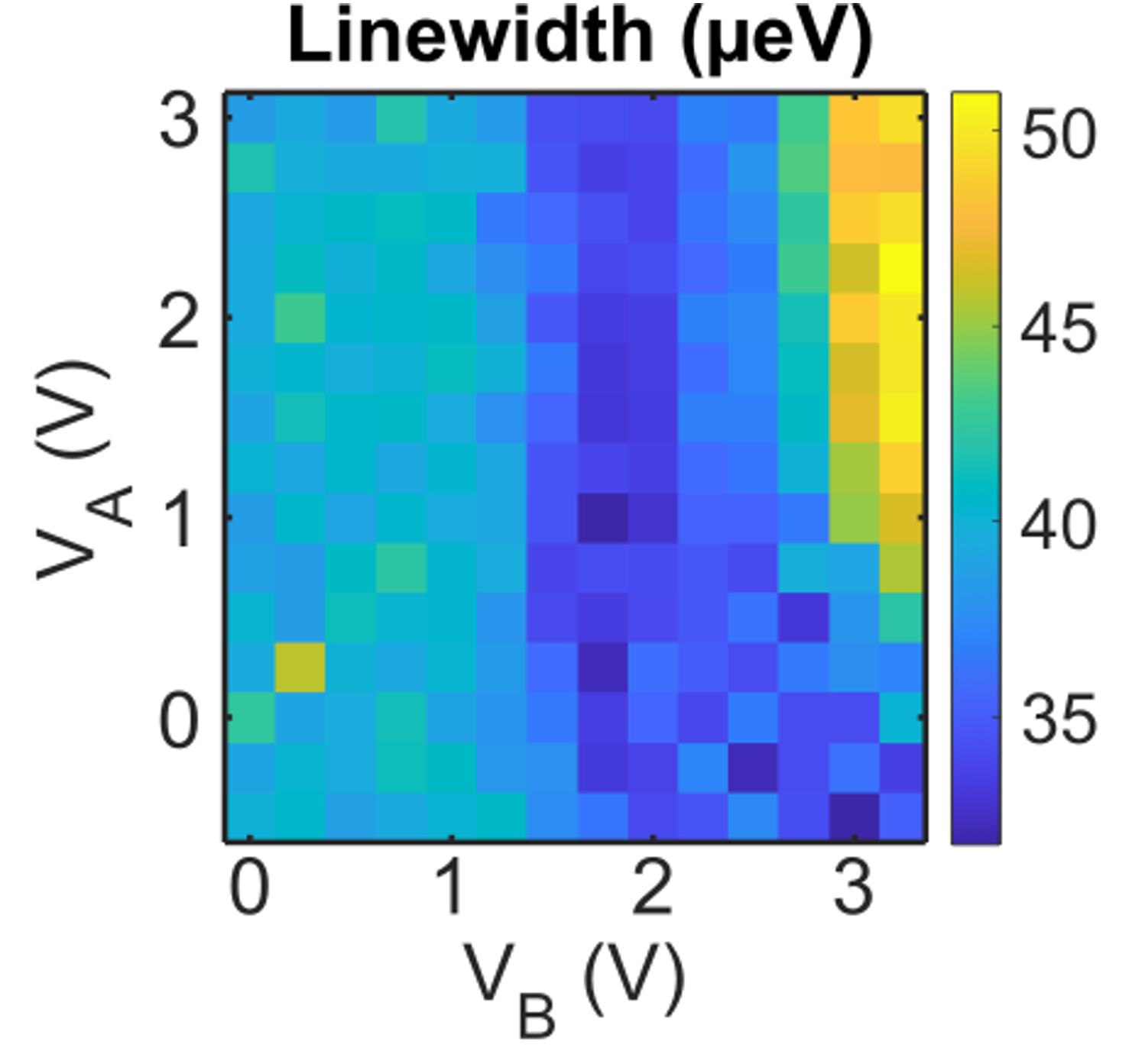
Finally, we underline that the method proposed to control the exciton FSS relies on a geometry very similar to the one already used to obtain highly indistinguishable photons under resonant excitation. This was reproducibly demonstrated from QDs deterministically positioned in micropillar cavities controlled by a single electrical pad Somaschi et al. (2016); Ollivier et al. (2020), in a large applied voltage range with limited current. We thus anticipate that the efficient and versatile control of the FSS obtained here in the non-passing regime would allow high indistinguishability. We note, however, that significant emission linewidth broadening is observed here in the passing regime ( V) in the present time-integrated measurements obtained under non-resonant excitation (see supplementary figure S3).
In conclusion, we have proposed a new scheme to control the exciton fine structure of a QD inside a micro-pillar cavity based on three independent electric potentials. Numerical simulations provide important insight on how the proposed geometry allows for a three-dimensional control of the electrical field at the center of the pillar cavity. Experimentally, we observe a tuning of the FSS in the 10-20 µeV range Trotta et al. (2014, 2015) which is shown to be sufficient to cancel the FSS of annealed InGaAs QDs. The mean-exciton energy is controlled over a significantly lower range than the one obtained for strain tuning techniques in bulk samples. However, several parameters can be explored to increase the amplitude of the electric field variation in the pillar center: length and width of the connecting ridges, vertical doping structures, etc. Here, we reported an 80 µeV exciton tuning range - a value that is already sufficient to tune the QD exciton into resonance with the pillar cavity mode when combined with the in-situ lithography technique Dousse et al. (2008). Indeed, this technique has been shown powerful to define a quasi-resonant pillar cavity around a chosen quantum dot for bright single photon sources or entangled photon pairs Somaschi et al. (2016); Dousse et al. (2010). Our work thus opens the path toward the fabrication of bright sources of single photons and entangled photon pairs, with control of both the QD-cavity detuning and the excitonic fine structure.
Acknowledgements
This work was partially supported by the H2020-FET OPEN project number 899544 - PHOQUSING, the French RENATECH network, and the European Research Council Starting Grant No. 715939, Nanophennec. H. O. acknowledges support from the Paris Ile-de-France Région in the framework of DIM SIRTEQ. M.E. acknowledges funding by the Deutsche Forschungsgemeinschaft (DFG, German Research Foundation) Project 401390650, and by the University of Oldenburg through a Carl von Ossietzky Young Researchers fellowship.
References
- Senellart et al. (2017) P. Senellart, G. Solomon, and A. White, Nature Nanotechnology 12, 1026 (2017).
- Schimpf et al. (2021) C. Schimpf, M. Reindl, F. Basso Basset, K. D. Jöns, R. Trotta, and A. Rastelli, Applied Physics Letters 118, 100502 (2021), https://doi.org/10.1063/5.0038729 .
- Jöns et al. (2017) K. D. Jöns, L. Schweickert, M. A. M. Versteegh, D. Dalacu, P. J. Poole, A. Gulinatti, A. Giudice, V. Zwiller, and M. E. Reimer, Scientific Reports 7, 1700 (2017).
- Bayer et al. (2002) M. Bayer, G. Ortner, O. Stern, A. Kuther, A. A. Gorbunov, A. Forchel, P. Hawrylak, S. Fafard, K. Hinzer, T. L. Reinecke, S. N. Walck, J. P. Reithmaier, F. Klopf, and F. Schäfer, Phys. Rev. B 65, 195315 (2002).
- Léger et al. (2007) Y. Léger, L. Besombes, L. Maingault, and H. Mariette, Phys. Rev. B 76, 045331 (2007).
- Benson et al. (2000) O. Benson, C. Santori, M. Pelton, and Y. Yamamoto, Physical Review Letters 84, 2513 (2000).
- Liu et al. (2019) J. Liu, R. Su, Y. Wei, B. Yao, S. F. C. d. Silva, Y. Yu, J. Iles-Smith, K. Srinivasan, A. Rastelli, J. Li, and X. Wang, Nature Nanotechnology 14, 586 (2019).
- Brash et al. (2015) A. J. Brash, L. M. P. P. Martins, F. Liu, J. H. Quilter, A. J. Ramsay, M. S. Skolnick, and A. M. Fox, Phys. Rev. B 92, 121301 (2015).
- Ollivier et al. (2020) H. Ollivier, I. Maillette de Buy Wenniger, S. Thomas, S. C. Wein, A. Harouri, G. Coppola, P. Hilaire, C. Millet, A. Lemaitre, I. Sagnes, O. Krebs, L. Lanco, J. C. Loredo, C. Antón, N. Somaschi, and P. Senellart, ACS Photonics 7, 1050 (2020).
- Stevenson et al. (2006) R. Stevenson, R. Young, P. Atkinson, K. Cooper, D. Ritchie, and A. Shields, Nature 439, 179 (2006).
- Young et al. (2005) R. J. Young, R. M. Stevenson, A. J. Shields, P. Atkinson, K. Cooper, D. A. Ritchie, K. M. Groom, A. I. Tartakovskii, and M. S. Skolnick, Physical Review B 72, 113305 (2005).
- Huo et al. (2013) Y. Huo, A. Rastelli, and O. Schmidt, Applied Physics Letters 102, 152105 (2013).
- Kowalik et al. (2005) K. Kowalik, O. Krebs, A. Lemaitre, S. Laurent, P. Senellart, P. Voisin, and J. A. Gaj, Applied Physics Letters 86, 041907 (2005).
- Gerardot et al. (2007) B. Gerardot, S. Seidl, P. Dalgarno, R. Warburton, D. Granados, J. García, K. Kowalik-Seidl, O. Krebs, K. Karrai, A. Badolato, and P. Petroff, Applied Physics Letters 90, 041101 (2007).
- Seidl et al. (2006) S. Seidl, M. Kroner, A. Hogele, and K. Karrai, Applied Physics Letters 88 (2006), 10.1063/1.2204843.
- Kuklewicz et al. (2012) C. Kuklewicz, R. Malein, P. Petroff, and B. Gerardot, Nano Letters 12, 3761 (2012).
- Gong et al. (2011) M. Gong, W. Zhang, G.-C. Guo, and L. He, Physical Review Letters 106, 227401 (2011).
- Plumhof et al. (2011) J. D. Plumhof, V. Krápek, F. Ding, K. D. Jöns, R. Hafenbrak, P. Klenovský, A. Herklotz, K. Dörr, P. Michler, A. Rastelli, and O. G. Schmidt, Physical Review B 83, 121302 (2011).
- Bennett et al. (2010) A. Bennett, M. Pooley, R. Stevenson, M. Ward, R. Patel, A. Giroday, N. Sköld, I. Farrer, C. Nicoll, D. Ritchie, and A. Shields, Nature Physics 6, 947 (2010).
- Trotta et al. (2012) R. Trotta, E. Zallo, C. Ortix, P. Atkinson, J. D. Plumhof, J. van den Brink, A. Rastelli, and O. G. Schmidt, Physical Review Letters 109, 147401 (2012).
- Trotta et al. (2015) R. Trotta, J. Martín-Sánchez, I. Daruka, C. Ortix, and A. Rastelli, Physical Review Letters 114, 150502 (2015).
- Huber et al. (2018) D. Huber, M. Reindl, S. F. Covre da Silva, C. Schimpf, J. Martín-Sánchez, H. Huang, G. Piredda, J. Edlinger, A. Rastelli, and R. Trotta, Physical Review Letters 121, 033902 (2018).
- Wang et al. (2016) H. Wang, Z.-C. Duan, Y.-H. Li, S. Chen, J.-P. Li, Y.-M. He, M.-C. Chen, Y. He, X. Ding, C.-Z. Peng, C. Schneider, M. Kamp, S. Höfling, C.-Y. Lu, and J.-W. Pan, Phys. Rev. Lett. 116, 213601 (2016).
- Somaschi et al. (2016) N. Somaschi, V. Giesz, L. De Santis, J. C. Loredo, M. P. Almeida, G. Hornecker, S. L. Portalupi, T. Grange, C. Antón, J. Demory, C. Gómez, I. Sagnes, N. D. Lanzillotti-Kimura, A. Lemaítre, A. Auffeves, A. G. White, L. Lanco, and P. Senellart, Nature Photonics 10, 340 (2016).
- Dousse et al. (2010) A. Dousse, J. Suffczyński, A. Beveratos, O. Krebs, A. Lemaitre, I. Sagnes, J. Bloch, P. Voisin, and P. Senellart, Nature 466, 217 (2010).
- Tomm et al. (2021) N. Tomm, A. Javadi, N. O. Antoniadis, D. Najer, M. C. Lobl, A. R. Korsch, R. Schott, S. R. Valentin, A. D. Wieck, A. Ludwig, and R. J. Warburton, Nature Nanotechnology (2021), 10.1038/s41565-020-00831-x.
- Moczała-Dusanowska et al. (2019) M. Moczała-Dusanowska, Ł. Dusanowski, S. Gerhardt, Y. M. He, M. Reindl, A. Rastelli, R. Trotta, N. Gregersen, S. Höfling, and C. Schneider, ACS Photonics, ACS Photonics 6, 2025 (2019).
- Gazzano et al. (2013) O. Gazzano, S. Michaelis de Vasconcellos, C. Arnold, A. Nowak, E. Galopin, I. Sagnes, L. Lanco, A. Lemaître, and P. Senellart, Nature Communications 4, 1425 (2013).
- Trotta et al. (2014) R. Trotta, J. Wildmann, E. Zallo, O. Schmidt, and A. Rastelli, Nano Letters 14, 3439 (2014).
- Dousse et al. (2008) A. Dousse, L. Lanco, J. Suffczynski, E. Semenova, A. Miard, A. Lemaitre, I. Sagnes, C. Roblin, J. Bloch, and P. Senellart, Physical Review Letters 101, 267404 (2008).
Supplementary Information:
Three-dimensional electrical control of the excitonic fine structure for a quantum dot in a cavity