2D-Motion Detection using SNNs with Graphene-Insulator-Graphene Memristive Synapses
Abstract
The event-driven nature of spiking neural networks makes them biologically plausible and more energy-efficient than artificial neural networks. In this work, we demonstrate motion detection of an object in a two-dimensional visual field. The network architecture presented here is biologically plausible and uses CMOS analog leaky integrate-and-fire neurons and ultra-low power multi-layer RRAM synapses. Detailed transistor-level SPICE simulations show that the proposed structure can accurately and reliably detect complex motions of an object in a two-dimensional visual field.
Index Terms:
RRAM, Synapse, LIF Neuron, Compact model, SNN, Motion DetectionI Introduction
In the field of computer vision, motion detection has been traditionally performed using machine learning algorithms on hardware that are themselves based on the von Neumann architecture. While modern-day microprocessors face the infamous memory bottleneck issue, these approaches often turn out to be power-hungry [1]. On the other hand, spiking neural networks (SNNs) emulate the dynamics of biological neural networks in electronic circuits and deliver low-power, inherently parallel computation. Event-driven computation thus becomes an alternative in realizing energy-efficient hardware for numerous cognitive tasks [2]. The emergence of novel non-volatile memory technologies like resistive random access memories (RRAMs) [3], phase change memories [4], and spin transfer torque RAMs [5] has further accelerated the development of SNNs.
Several techniques have been proposed in the past for motion detection using SNNs [6, 7, 8, 9, 10, 11]. In [6], a novel temporal coding scheme is used to encode the real-time motion into a series of spikes and a gradient descent learning algorithm is utilized to train the two-layered SNN. An autonomous neuromorphic agent that could perform obstacle-avoidance and target acquisition was demonstrated using the CMOS-based ROLLS neuromorphic processor in [7]. Various studies such as probabilistic feed-forward synapses [9], rate-based Hebbian learning [10] and spike timing-dependent plasticity [11] have been proposed to realize directional selectivity and consequently motion detection. On the other hand, considering biological neural systems’ high efficacy and accuracy, authors in [12] have shown insect-inspired elementary motion detection. It is envisaged that the ability to mimic an insect’s navigation system would have a significant impact on the field of robotics, compact visual surveillance, etc., due to the limited computational capacity of their on-board processor.
In our effort to develop biologically inspired, low power motion detection framework, we improve and extend the delay and correlate network presented in [12] to detect complex motions. Our proposed SNN based network uses CMOS-based analog leaky integrate-and-fire (LIF) neurons and ultra-low-power, forming-free RRAMs as synapses. We present an end-to-end SPICE implementation of the complete network using an experimentally validated physics-based Verilog-A model of the synapse and transistor-level implementations for the neurons. We improve the network’s directional resolution by incorporating lateral inhibition. Also we show that the network can detect a wide range of input signal frequencies by adding an appropriate number of output neurons per direction.
This paper is organized as follows. Section II details the network architecture. Section III discusses the physics-based compact model of the GIG synapse, LIF neuron circuit, and peripheral circuitry used for stimulus generation. Section IV presents the simulation results followed by a conclusion in section V.
II Network Architecture
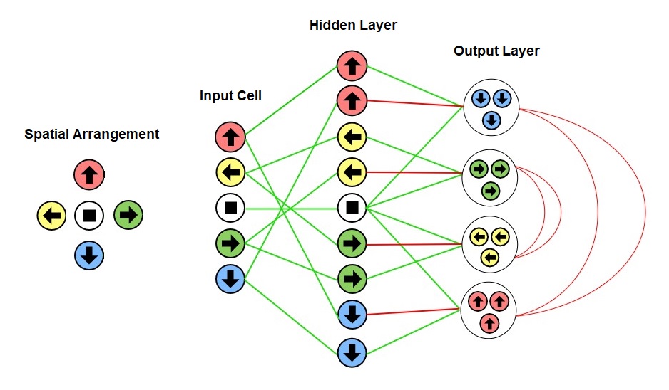
To detect the motion of an object moving along a particular direction, a delay and correlate network was presented in [12]. Basically, the idea is to introduce a temporal delay between two spatially adjacent inputs followed by a downstream mechanism for detecting the spatio-temporal correlations. Here, we modify the network presented in [12] to network shown in Fig. 1. Spatial arrangement of the input layer of a unit cell is shown in Fig. 1 (Left). The neuron at the center (white circle) is called a neutral neuron as it is not pointing in any of the cardinal directions. Neurons in the input layer are connected to the output layer neurons through a hidden layer as shown in Fig. 1. We introduce lateral inhibition (shown by red lines) between Up-Down and Left-Right output neurons to emphasize the fact that an object can’t move in Up-Down or Left-Right direction at the same time. This modification reduces the spiking activity for output neurons that are not meant to fire for given excitation and improve the network accuracy. Additionally, in order to make the network capable of detecting objects moving with a wide range of frequencies, we use N (instead of using a single) output neurons per direction. The value of N and time constants of each output neuron can be adjusted to meet the application-specific requirements.
The operation of the network shown in Fig. 1 is explained below. Input layer neurons denote the spatial activity of the object in the visual field and encode this activity by introducing a temporal delay between activity in spatially adjacent regions. This information from the input layer is passed on to the hidden layer through synapses. The adjustment of time constants of hidden layer neurons coupled with information received from the input layer generates a unique spatio-temporal pattern, encoding the spatial activity at the input layer. In this case, the time constant of the neutral neuron is made smaller than the other four neurons. Finally, the spatio-temporal pattern generated at the hidden layer is transmitted to the output layer. The incoming spikes to the output layer may have an excitatory (green lines) or inhibitory (red lines) effect on the output layer. The output layer neurons are designed with threshold voltages and time constants such that they will fire if they receive two consecutive excitatory spikes within a short time interval. However, if an inhibitory spike is received shortly before the first spike, then the membrane voltage is reduced sufficiently and the excitatory pair of spikes does not cause an output spike.
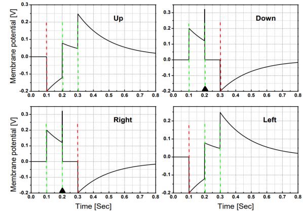
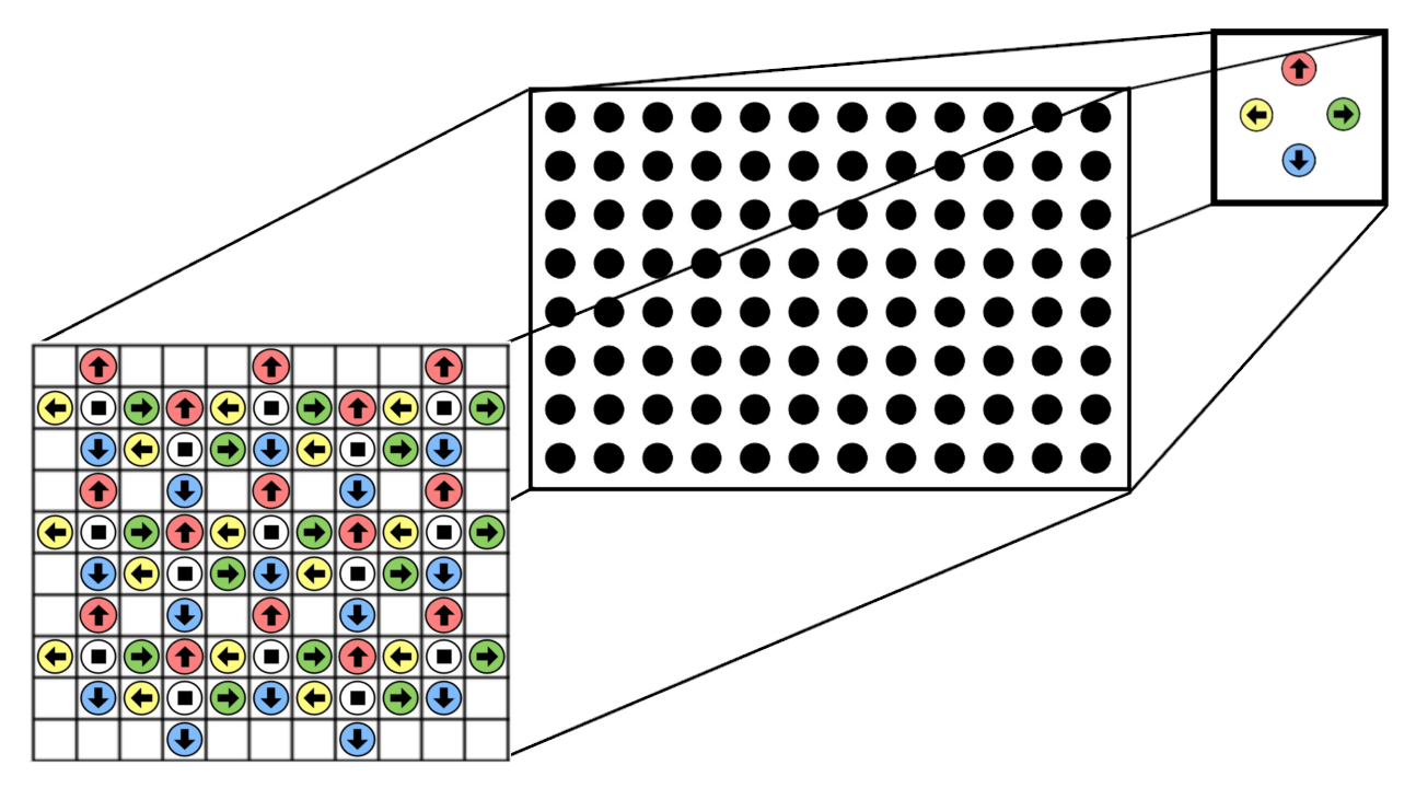
Fig. 2 illustrates the working of the unit cell when the object moves in a specific direction across an input cell, say, diagonally from Left-Up to Right-Down. The input neurons get excited in the order: Left and Up; Center; Right and Down. The temporal delays in the activity at spatially adjacent location are encoded at the input layer and coupled with time constant adjustments of the hidden layer neurons, which results in a spike pattern at the output neuron as follows: Down and Right receive two excitatory spikes followed by one inhibitory. Up and Left receive one inhibitory spike followed by two excitatory. Hence, the Right and Down neurons spike for this input while the other two do not. The input cell shown in Fig. 1 is used to tessellate the 1011 visual field as shown in Fig. 3. Each of the 15 input cells has its own patch of hidden layer neurons which connects to a common output layer as shown in Fig. 4. The network uses a total of 75 input neurons, 135 hidden neurons, and 4N output neurons, where N was varied from 1 to 5 for performance comparison. A total of 315 synapses are required to realize the connections between the neurons.
III SPICE Implementation
III-A Synapse Model
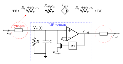
Resistive random-access memory technology has emerged in the last decade as a promising candidate for applications in non-volatile storage as well as for neuromorphic computation [13, 14, 15, 16, 17, 18]. ”Forming-free” operation with ultra-low operating current has been previously observed in graphene-insulator-graphene (GIG) RRAM devices with chemical vapor deposited (CVD) graphene electrodes [19]. The switching material for the GIG device is a three-layer stack of TiOx, Al2O3, and TiO2. The incorporation of CVD-grown graphene as electrodes significantly reduces the operating current compared to conventional electrodes such as TiN. The ultra-low ON and OFF state currents (180 nA and 100pA, respectively) and the ON-state non-linearity make these devices highly desirable for high-density storage and compute-in-memory applications. For a detailed discussion of GIG device fabrication and characterization, see [19]. A physics-based SPICE-compatible compact model to make this device suitable for large-scale circuits and systems design can be found here [20]. The electrical equivalent schematic of the RRAM used for the simulation is shown in Fig. 5 (top). The model framework assumes the existence of a pre-formed filament(s) in the top TiO2 and the bottom TiOx layers because of the forming-free nature of the device. The total series resistance offered by graphene electrode and TiO2 layer is modeled as a lumped resistor of value Rgr + R. The resistive switching behavior in this device is attributed to the formation and rupture of a conductive filament in the Al2O3 layer, and it is modeled as a series connection of variable resistor (R) and dependent current source (Igap). For more details about the model formulation, we direct readers to [20].
III-B Analog LIF neuron
The LIF neuron model is one of the most widely used models owing to its computational efficiency and biological plausibility [21]. The LIF model consists of a parallel combination of a resistor (R) and an integrating capacitor (C), as shown in Fig. 5. The currents Iin coming from the synapses, connected at the input terminal of the LIF neuron, charge up the capacitor. Each spiking neuron is characterized by an internal state variable, the membrane potential Vm(t). When this membrane potential exceeds a fixed threshold (Vth), a spike is sent out, and the capacitor is discharged to a reset potential (Vreset) using the voltage-controlled NMOS switch. A comparator and a delay block are used to generate the constant-width output spikes. The neuron block is implemented using TSMC’s 180nm CMOS standard cell library.
III-C Stimulus Generation
The input spikes denoting the motion of the object are generated using a peripheral circuit that mimics a dynamic vision sensor (DVS). Each pixel in a DVS is sensitive to relative temporal contrast in the luminous intensity, and upon detection of a sufficiently significant change, it sends out a spike [22]. To emulate this behavior, we treat each event as a vector , where and define the pixel location in the visual field, and is the time of the event. The trajectory of the moving object is modeled using the appropriate mathematical function and it is used to excite the input layer.
IV Results
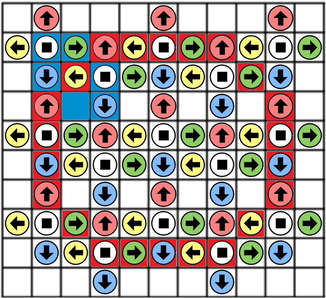
A SPICE simulation of the network shown in Fig. 4 is done using Cadence Virtuoso [23]. The object is assumed to be a square block of 33 pixels, shown in blue in Fig. 3. The red color denotes the circular path followed by the object’s center.
Whenever the object is at a specific location, all neurons that the object covers produce a spike that propagates through the deeper layers of the network as shown in Fig. 4. We expect a significant increase in the firing activity of the output neuron
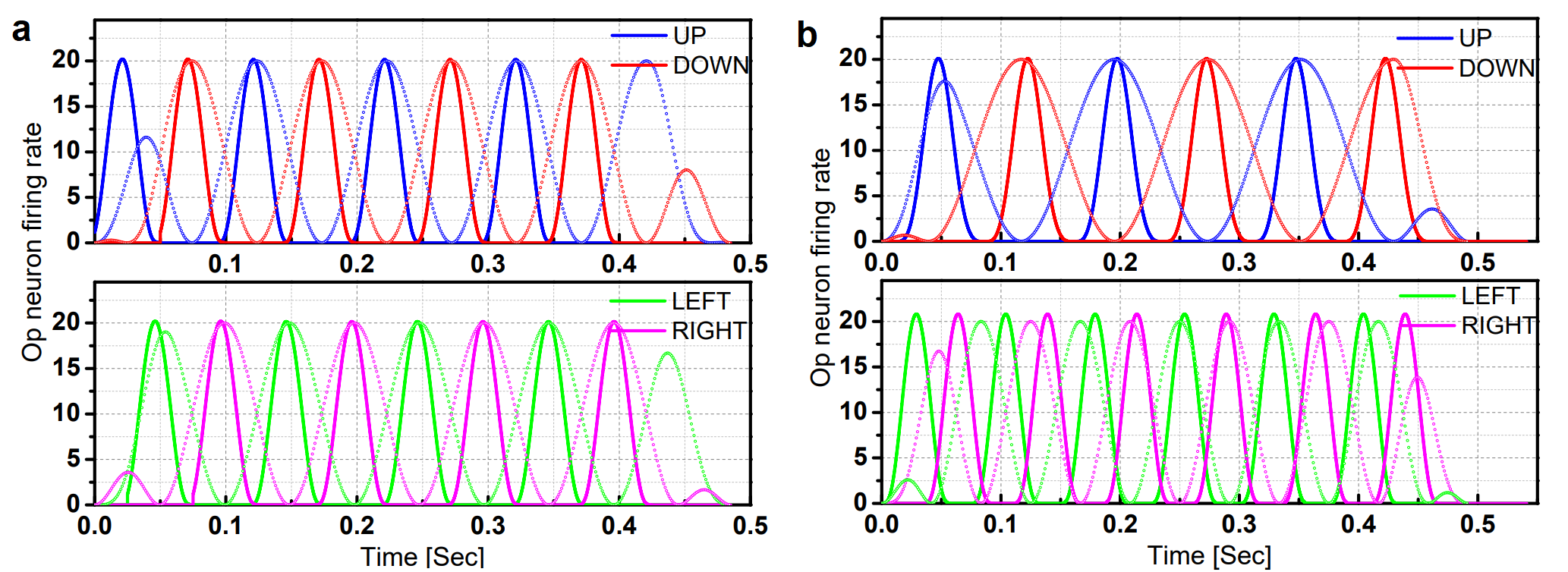
when the object moves across the visual field along its corresponding direction. The output firing rates for circular and eight-shaped trajectories are shown in Fig. 6.
For a circular input path, the four output neurons produce sinusoidal firing rates, with relative phase lags of 90∘ between them, as shown in Fig. 6(a). This can be understood by considering the UP-DOWN and LEFT-RIGHT neuron pairs as two orthogonal basis elements encoding the direction of motion. The stimulus travels rightwards from 0 to T/2, leftwards from T/2 to T, upwards from 3T/4 to T/4, and downwards from T/4 to 3T/4 where T is the time period. The firing rates of the corresponding output neuron reach their maxima at the midpoint of the time intervals mentioned above. Similarly, for an eight-shaped input path, the firing rate of the UP-DOWN neurons is half of that of the LEFT-RIGHT neurons. Here, the stimulus makes two oscillations along the horizontal direction for every oscillation along the vertical direction as shown in Fig. 6(b).
The instantaneous firing rate () is calculated by filtering the spike trains using a low-pass filter as
| (1) |
where * denotes the convolution operation. refers to the spike train (a sequence of impulses at the locations of the spikes) and refers to the impulse response of the aforementioned filter with and as constants that are set to the mean and twice the mean of the output neuron time constants. is a normalization constant and is the unit step function.
The ideal spiking rates () corresponding to four output neurons are obtained from the parameterization () of the path for considered trajectories (circular and eight shaped) as
| (2) |
where takes on four values depending on the output channel (UP, DOWN, LEFT, RIGHT). For UP and DOWN (LEFT and RIGHT), the directional velocity and its maximum value are replaced by and ( and ), respectively. Here is the maximum firing rate of the output neurons. The ideal firing rates reach their maximum when the object moves at maximum velocity along the preferred direction and go to zero when the object moves against the preferred direction. In case of no movement either along or against, they settle to half the maximum rate. The firing rate obtained from SPICE simulations (solid lines) is showing a good level of match with the ideal firing rate (dotted lines) as shown in Fig. 6.
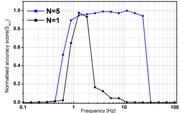
In order to make the network sensitive to a wide range of moving object frequencies, we use N output neurons (instead of one neuron) per direction. The network with five output neurons per direction, with time constants being logarithmically distributed from 5 ms to 500 ms, performs better than the network with one output neuron per direction, with a 500 ms time constant. The accuracy score () is shown in Fig. 7 as a function of the rotation frequency for the circular input case. The accuracy score is calculated as
| (3) |
A network designed with an appropriate value of N will be able to identify the required range of moving object frequency.
.
V Conclusion
We have demonstrated end-to-end SPICE simulation of SNN based motion detection framework. We design our network using an experimentally validated physics based synapse model and transistor-level implementation of LIF neurons. We demonstrated improvement in network performance by including lateral inhibition and pool of N output neurons per direction. The proposed network can accurately encode the object’s direction and velocity of movement over a significant range of velocities. A notably similar area where the same network can be applied is event-based tactile sensing where the stimulus is localized and moves at relatively low velocities across the sensory field. The network can help to extract velocity information directly from the input for using in higher-level applications like handwriting recognition. Tactile sensing data-sets such as the ST-MNIST digits data-set [24] provide a good target case for this network architecture beyond its original intended application. Other future work also includes the processing of Braille character data collected using tactile neuromorphic sensors.
References
- McKee [2004] S. A. McKee. Reflections on the memory wall. Association for Computing Machinery, 2004. doi: 10.1145/977091.977115.
- Mehonic et al. [2020] A. Mehonic, A. Sebastian, B. Rajendran, O. Simeone, E. Vasilaki, and A. J. Kenyon. Memristors—from in-memory computing, deep learning acceleration, and spiking neural networks to the future of neuromorphic and bio-inspired computing. Advanced Intelligent Systems, 2(11):2000085, 2020. doi: 10.1002/aisy.202000085.
- Yu [2018] S. Yu. Neuro-inspired computing with emerging nonvolatile memorys. Proceedings of the IEEE, 106(2):260–285, 2018. doi: 10.1109/JPROC.2018.2790840.
- Gallo and Sebastian [2020] M. L. Gallo and A. Sebastian. An overview of phase-change memory device physics. Journal of Physics D: Applied Physics, 53(21):213002, mar 2020. doi: 10.1088/1361-6463/ab7794.
- Bhatti et al. [2017] S. Bhatti, R. Sbiaa, A. Hirohata, H. Ohno, S. Fukami, and S.N. Piramanayagam. Spintronics based random access memory: a review. Materials Today, 20(9):530–548, 2017. ISSN 1369-7021. doi: 10.1016/j.mattod.2017.07.007.
- Yang et al. [2018] J. Yang, Q. Wu, M. Huang, and T. Luo. Real time human motion recognition via spiking neural network. 366:012042, jun 2018. doi: 10.1088/1757-899x/366/1/012042.
- Milde et al. [2017] M. B. Milde, H. Blum, A. Dietmüller, D. Sumislawska, J. Conradt, G. Indiveri, and Y. Sandamirskaya. Obstacle avoidance and target acquisition for robot navigation using a mixed signal analog/digital neuromorphic processing system. Frontiers in Neurorobotics, 11:28, 2017. ISSN 1662-5218. doi: 10.3389/fnbot.2017.00028.
- Orchard et al. [2013] G. Orchard, R. Benosman, R. Etienne-Cummings, and N. V. Thakor. A spiking neural network architecture for visual motion estimation. In 2013 IEEE Biomedical Circuits and Systems Conference (BioCAS), pages 298–301, 2013. doi: 10.1109/BioCAS.2013.6679698.
- Buchs and Senn [2001] N. J. Buchs and W. Senn. Learning direction selectivity through spike-timing dependent modification of neurotransmitter release probability. Neurocomputing, 38:121–127, 2001.
- Feidler et al. [1997] J. C. Feidler, A. B. Saul, A. Murthy, and A. L. Humphrey. Hebbian learning and the development of direction selectivity: the role of geniculate response timings. Network: Computation in Neural Systems, 8(2):195–214, jan 1997. doi: 10.1088/0954-898x_8_2_006.
- Buchs and Senn [2002] N. J. Buchs and W. Senn. Spike-based synaptic plasticity and the emergence of direction selective simple cells: simulation results. Journal of computational neuroscience, 13(3):167–186, 2002.
- Dalgaty et al. [2018] T. Dalgaty, E. Vianello, D. Ly, G. Indiveri, B. Salvo, E. Nowak, and J. Casas. Insect-Inspired Elementary Motion Detection Embracing Resistive Memory and Spiking Neural Networks, pages 115–128. 07 2018. ISBN 978-3-319-95971-9. doi: 10.1007/978-3-319-95972-6_13.
- et al. [2008] H. Y. Lee et al. Low power and high speed bipolar switching with a thin reactive ti buffer layer in robust hfo2 based rram. In 2008 IEEE International Electron Devices Meeting, pages 1–4, 2008. doi: 10.1109/IEDM.2008.4796677.
- et al. [2011] S. S. Sheu et al. A 4mb embedded slc resistive-ram macro with 7.2ns read-write random-access time and 160ns mlc-access capability. In 2011 IEEE International Solid-State Circuits Conference, pages 200–202, 2011. doi: 10.1109/ISSCC.2011.5746281.
- et al. [2009] S. S. Sheu et al. A 5ns fast write multi-level non-volatile 1 k bits rram memory with advance write scheme. In 2009 Symposium on VLSI Circuits, pages 82–83, 2009.
- et al. [2012] S. R. Lee et al. Multi-level switching of triple-layered taox rram with excellent reliability for storage class memory. In 2012 Symposium on VLSI Technology (VLSIT), pages 71–72, 2012. doi: 10.1109/VLSIT.2012.6242466.
- Chakrabarti et al. [2017] B. Chakrabarti, M. Lastras-Montaño, G. Adam, M. Prezioso, B. Hoskins, K-T Cheng, and D. Strukov. A multiply-add engine with monolithically integrated 3d memristor crossbar/cmos hybrid circuit. Scientific Reports, 7:42429, 02 2017. doi: 10.1038/srep42429.
- Adam et al. [2017] G. C. Adam, B. D. Hoskins, M. Prezioso, F. Merrikh-Bayat, B. Chakrabarti, and D. B. Strukov. 3-d memristor crossbars for analog and neuromorphic computing applications. IEEE Transactions on Electron Devices, 64(1):312–318, 2017. doi: 10.1109/TED.2016.2630925.
- Chakrabarti et al. [2014] B. Chakrabarti, T. Roy, and E. M. Vogel. Nonlinear switching with ultralow reset power in graphene-insulator-graphene forming-free resistive memories. IEEE Electron Device Letters, 35(7):750–752, 2014. doi: 10.1109/LED.2014.2321328.
- Reddy et al. [2021] L. H. Reddy, S. Pande, T. Roy, E. M. Vogel, A. Chakravorty, and B. Chakrabarti. A spice compact model for forming-free, low-power graphene-insulator-graphene reram technology. Emergent Materials, 4:1055 – 1065, 2021.
- Tang et al. [2014] T. Tang, R. Luo, B. Li, H. Li, Y. Wang, and H. Yang. Energy efficient spiking neural network design with rram devices. In 2014 International Symposium on Integrated Circuits (ISIC), pages 268–271, 2014. doi: 10.1109/ISICIR.2014.7029565.
- Lichtsteiner et al. [2006] Patrick Lichtsteiner, Christoph Posch, and Tobi Delbruck. A 128x128 120 db 15s latency asynchronous temporal contrast vision sensor. 2006.
- [23] Cadence® Virtuoso. URL https://www.cadence.com/en_US/home.html.
- et al. [2020] H. H. See et al. ST-MNIST - the spiking tactile mnist neuromorphic dataset. ArXiv, abs/2005.04319, 2020.