The Silicon Vertex Detector of the Belle II Experiment
Abstract
In 2019 the Belle II experiment started data taking at the asymmetric SuperKEKB collider (KEK, Japan) operating at the Y(4S) resonance. Belle II will search for new physics beyond the Standard Model by collecting an integrated luminosity of 50 ab-1. The silicon vertex detector (SVD), consisting of four layers of double-sided silicon strip sensors, is one of the two vertex sub-detectors. The SVD extrapolates the tracks to the inner pixel detector (PXD) with enough precision to correctly identify hits in the PXD belonging to the track. In addition the SVD has standalone tracking capability and utilizes ionization to enhance particle identification in the low momentum region. The SVD is operating reliably and with high efficiency, despite exposure to the harsh beam background of the highest peak-luminosity collider ever built. High signal-to-noise ratio and hit efficiency have been measured, as well as the spatial resolution; all these quantities show excellent stability over time. Data-simulation agreement on cluster properties has recently been improved through a careful tuning of the simulation. The precise hit-time resolution can be exploited to reject out-of-time hits induced by beam background, which will make the SVD more robust against higher levels of background. During the first three years of running, radiation damage effects on strip noise, sensor currents and depletion voltage have been observed, as well as some coupling capacitor failure due to intense radiation bursts. None of these effects cause significant degradation in the detector performance.
1 Introduction
Belle II [1] is a high energy physics experiment at the intensity frontier searching for physics beyond the Standard Model in rare meson, charm and tau decays. Since 2019, it has been operating at the asymmetric collider SuperKEKB [2] at Tsukuba in Japan. This collider operates primarily at the centre-of-mass energy corresponding to the mass (10.58 GeV) and it is designed to reach an instantaneous luminosity of cm-2 s-1 and to deliver a ab-1 dataset. It already holds the world luminosity record of cm-2 s-1. Essential features required to reach Belle II physics goals are the precise determination of the decay vertices, accurate and efficient tracking capabilities, including low-momentum particles, and the capability to distinguish between the different kinds of charged particles.
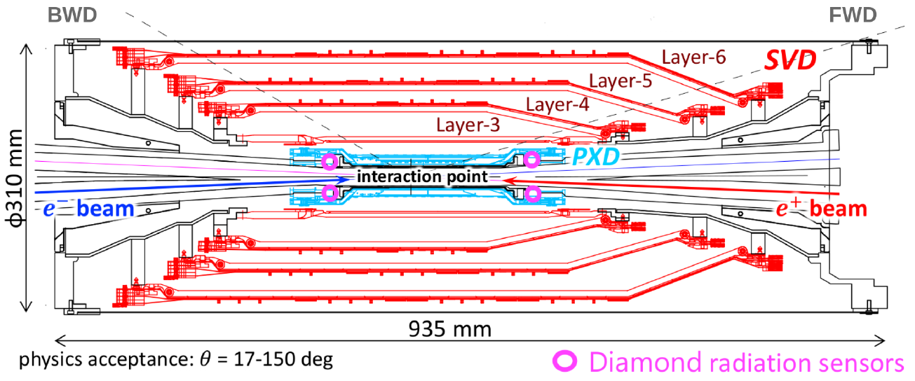
The Belle II experiment is an upgrade of the Belle the detector. Its design has been conceived to allow similar or better performance than Belle in an harsher environment characterised by an higher beam background and Lorentz boost reduced from to . The vertex detector of Belle II is designed to provide a better resolution than the Belle silicon vertex detector [3] in order to compensate for the reduced Lorentz boost. This improvement is achieved with more precise point resolution, a reduced inner radius and a low material budget. Moreover it must operate in a high background environment with a hit rate of 20 (3) MHz/cm2 and an integrated yearly dose of 2 (0.2) Mrad at a radius of 14 (40) mm. Figure 1 shows the cross-section view of the Belle II vertex detector. It is composed of two layers of DEPFET pixel sensors (PXD), with the innermost layer at 1.4 cm from the interaction point, and four layers of double-sided silicon strip sensors (SVD).
2 The Belle II silicon strip vertex detector
The SVD detector [4] consists of four layers numbered 3, 4, 5 and 6 from lower to higher radius, which are composed of seven, ten, twelve and sixteen ladders with two, three, four and five sensors, respectively. Its material budget is 0.7% of the radiation length per layer on average. Diamond sensors are installed on the beam pipe for radiation monitoring and to trigger fast beam aborts [5]. The SVD detector has three specific roles: firstly it allows to extrapolate the tracks toward the PXD; this is essential for the reconstruction of decay vertices and also to define regions of interest to reduce the PXD data transfer rate. Secondly it provides stand-alone tracking for low momentum tracks and finally it contributes to the particle identification by providing the information about the ionization energy loss.
The SVD detector is composed of 172 double-sided silicon strip sensors covering an area of 1.2 m2 for a total of 224 thousand strips. Each sensor is based on an N-type bulk about 320 m thick. The two opposite sides are implanted with P- and N-doped sensitive strips. The metal readout strips are AC coupled and are placed on top of the implanted strips, separated by a dielectric SiO2. Each readout channel is connected to a single strip. Between every two readout strips there is a floating strip that is not read out. The two sensor sides are referred to as the u/P and the v/N sides and have strips parallel and orthogonal to the beam direction, respectively. Layer 3 is equipped with mm mm sensors with a pitch of 50 (160) m for the u/P (v/N) side. Layers 4, 5 and 6 are equipped with mm mm rectangular sensors with a pitch of 75 (240) m in u/P (v/N) and with trapezoidal slanted sensors mm long, with a width varying from 41 to 61 mm and a pitch varying from 50 to 75 m in u/P and a 240 m pitch in v/N. The sensor full-depletion voltage is between 20 and 60 V and the operation voltage is 100 V. The rectangular sensors have been produced by Hamamatsu Photonics while Micron Semiconductor produced the trapezoidal slanted ones.
The SVD front-end readout ASIC is the APV25 chip [6]. It was originally developed for the CMS silicon tracker. It has 128 channel inputs per chip, a short shaping time of 50 ns, its power consumption is 0.4 W per chip and it can tolerate more than 100 Mrad of radiation dose. It operates in a multi-peak mode at 32 MHz, and not at the bunch crossing frequency, which is about eight times larger. To reconstruct the output waveform of each channel, six subsequent analog samples are recorded. A mixed three/six acquisition mode has also been prepared to reduce dead time, data size and occupancy at higher luminosity. The readout chips of the middle sensors are directly installed on one side of the sensor to minimise the signal propagation length and reduce the capacitance and the noise. These chips are thinned to 100 m to reduce the material budget and are cooled down using bi-phase CO2 at -20∘ C. A wrapped flex also allows the read out of the side of the sensor opposite to the chip position.
3 Operation and performance
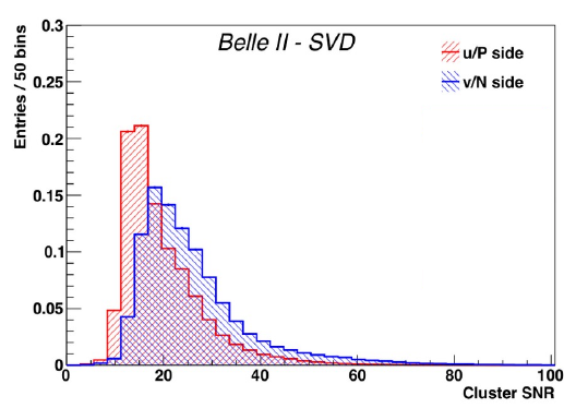
The SVD detector has been installed in 2018 and has been operated since 2019. The operation has been reliable and smooth. The total fraction of masked strips is about , moreover the average sensor hit efficiency is greater than and stable with time. The collected signal charge, normalised for the length of traversed sensor thickness, is similar in all sensors and matches the expectations. In the u/P side the charge is in agreement with the expectations from a minimal ionising particle taking into account the uncertainty in the APV25 gain calibration (). In the v/N side there is a signal loss due to the large pitch and the presence of the floating strip. A very good signal-to-noise ratio is observed in all 172 sensors with a most probable value between 13 to 30. The u/P side presents a larger noise due to the longer strip length and the larger inter-strip capacitance. The signal instead depends strongly by the sensor position due to the track incidence angle. Figure 2 shows the collected signal charge, normalised for the length of traversed sensor thickness and the signal-to-noise ratio for the more backward sensors of layer 3, summed over all ladders.

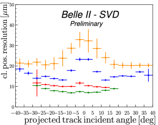
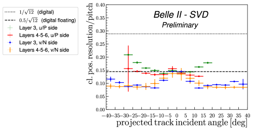
The cluster position resolution has been measured using events. It is estimated from the residuals of the cluster position with respect to the unbiased track intercept after the effect of the track extrapolation error has been subtracted. The measured resolutions are in agreement with the expectations from the pitch and are approximately 9 m for layer 3 u/P side, 11 m for layer 4, 5 and 6 u/P side, 20 m for layer 3 v/N side and 25 m for layer 4, 5 and 6 v/N side. Figure 3 shows the distributions, with respect to the projected track incident angle, of the resolution and of the resolution normalised to the pitch.
The hit time resolution with respect to the event time provided by the Belle II central drift chamber is approximately 2.9 ns for the u/P side and 2.4 ns for the v/N side. This excellent hit time resolution can be exploited to efficiently reject off-time hits coming from the beam background. Preliminary studies show that it is possible to reject about half of the background hits keeping more than of the signal ones. This information, not yet used, will be exploited at higher luminosities and background levels.
4 Beam background and radiation effects
Beam background produces radiation damage in the sensors and increases the SVD hit occupancy. A higher hit occupancy degrades the tracking performance by increasing the number of clusters that can be erroneously associated to tracks or even create fake tracks in the reconstruction. The present occupancy limit, set by performance studies, is about in layer 3. This limit could be approximately doubled by exploiting the hit time information to reject off-time background hits. With the current luminosity the average hit occupancy in layer 3 is less than . It however reaches at the design luminosity of cm-2 s-1 according to beam background projections based on scaling the simulation with a data-simulation ratio. This corresponds to a dose of 0.2 Mrad per year and a 1 MeV neutron equivalent fluence of neq/cm2 per year. These long term beam background extrapolations are affected by large uncertainties related to the collimation and the injection background that is not yet included. The integrated dose on the SVD sensors is evaluated exploiting the correlation between the measured occupancy and the dose rate measured in the diamond sensors [5]. This estimate is based on several assumptions and has an uncertainty of about . The mid plane of layer 3 is the detector region the most exposed to radiation. The estimated dose collected by this region over the past two and a half years is 70 krad. This corresponds to a fluence of neq/cm2, where the ratio of neq/cm2/krad between dose and neq fluence was estimated from simulation.
The first effects of radiation damage are already visible. The increase of leakage currents are proportional to the sensor bulk damage due to non-ionising energy loss. This damage, according to the NIEL hypothesis [7], is proportional to the 1 MeV neutron equivalent fluence, which in turn is proportional to the integrated dose. This linear correlation between leakage current and integrated dose is observed for all sensors with slopes in the range 2 to 5 A/cm2/Mrad. These values are of the same order of magnitude as those observed by the BaBar experiment: 1 A/cm2/Mrad at 20∘C [8]. In the SVD the leakage current contribution to the noise is highly suppressed by the short shaping time of the APV25 chips. Therefore, it will not affect significantly the total strip noise even after ten years at design luminosity, corresponding to about 2 Mrad of dose with present background extrapolation. It however will become comparable with present noise after about ten Mrad. Sensor bulk damage due to non-ionising energy loss can also change the depletion voltage. The depletion voltage can be monitored by measuring the v/N side noise as a function of the operation voltage: since the substrate of the sensor is N-type, the v/N-side strips are completely isolated, and hence their noise drops, at full depletion. No change in the full depletion voltage has yet been observed, in agreement with the low integrated 1 MeV neutron equivalent fluence accumulated. Another radiation effect is the increase of strip noise due to the ionising energy loss that causes fixed oxide charges in the SiO2 layer increasing the inter-strip capacitance. The amount of fixed oxide charges and hence the noise increase is expected to saturate. A noise increase of 20-25% has been observed in layer 3. The saturation has been reached in the v/N side and is being reached in the u/P side after 70 krad. No impact on performances is observed due to this increase of the strip noise.
5 Conclusion
The Belle II SVD detector has been taking data since March 2019 smoothly and reliably, showing excellent performance in agreement with the expectations. The first effects of radiation damage have been observed at the expected level and they are not affecting the performance. The detector is ready to cope with the increased beam background expected during future running.
Acknowledgments
This project has received funding from the European Union’s Horizon 2020 research and innovation programme under the Marie Sklodowska-Curie grant agreements No 644294 and 822070. This work is supported by MEXT, WPI, and JSPS (Japan); ARC (Australia); BMBWF (Austria); MSMT (Czechia); L’Institut National de Physique Nucléaire et de Physique des Particules (IN2P3) du CNRS (France); AIDA-2020 (Germany); DAE and DST (India); INFN (Italy); NRF and RSRI (Korea); and MNiSW (Poland).
References
- [1] Belle II collaboration, Belle II Technical Design Report, arXiv:1011.0352.
- [2] Y. Ohnishi et al., Accelerator design at SuperKEKB, PTEP 2013 (2013) 03A011.
- [3] Z. Natkaniec et al., Status of the Belle silicon vertex detector, Nucl. Instrum. Meth. A 560 (2006) 1.
- [4] K. Adamczyk et al., The Design, Construction, Operation and Performance of the Belle II Silicon Vertex Detector, arXiv:2201.09824.
- [5] S. Bacher et al., Performance of the diamond-based beam-loss monitor system of Belle II, Nucl. Instrum. Meth. A 997 (2021) 165157 [arXiv:2102.04800].
- [6] M.J. French et al., Design and results from the APV25, a deep sub-micron CMOS front-end chip for the CMS tracker, Nucl. Instrum. Meth. A 466 (2001) 359.
- [7] ROSE collaboration, Developments for radiation hard silicon detectors by defect engineering - Results by the CERN RD48 (ROSE) Collaboration, Nucl. Instrum. Meth. A 465 (2000) 60.
- [8] BaBar collaboration, The BABAR Detector: Upgrades, Operation and Performance, Nucl. Instrum. Meth. A 729 (2013) 615 [arXiv:1305.3560].