Rising speed limits for fluxons via edge quality improvement in wide MoSi thin films
Abstract
Ultra-fast vortex motion has recently become a subject of extensive investigations, triggered by the fundamental question regarding the ultimate speed limits for magnetic flux quanta and enhancements of single-photon detectors. In this regard, the current-biased quench of a dynamic flux-flow regime – flux-flow instability (FFI) – has turned into a widely used method for the extraction of information about the relaxation of quasiparticles (unpaired electrons) in the superconductor. However, the large relaxation times deduced from FFI for many superconductors are often inconsistent with the fast relaxation processes implied by their single-photon counting capability. Here, we investigate FFI in nm-thick m-wide MoSi strips with rough and smooth edges produced by laser etching and milling by a focused ion beam. For the strip with smooth edges we deduce, from the current-voltage (-) curve measurements, a factor of 3 larger critical currents , a factor of 20 higher maximal vortex velocities of 20 km/s, and a factor of 40 shorter . We argue that for the deduction of the intrinsic of the material from the - curves, utmost care should be taken regarding the edge and sample quality and such a deduction is justified only if the field dependence of points to the dominating edge pinning of vortices.
I Introduction
Ultra-fast vortex motion in superconductors has recently attracted great attention both experimentally Embon et al. (2017); Rouco et al. (2018); Dobrovolskiy et al. (2019a); Leo et al. (2020); Dobrovolskiy et al. (2020a); Ustavschikov et al. (2020) and theoretically Vodolazov (2019); Bezuglyj et al. (2019); Kogan and Prozorov (2020); Pathirana and Gurevich (2020); Kogan and Nakagawa (2021); Pathirana and Gurevich (2021). This attention is triggered by the fundamental question regarding the ultimate speed limit for magnetic flux transport via superconducting vortices and the phenomena of generation of sound Ivlev et al. (1999); Bulaevskii and Chudnovsky (2005) and spin waves Bespalov et al. (2014); Dobrovolskiy et al. (2021) by fluxons moving at velocities of a few km/s. Furthermore, high-velocity vortex dynamics is essential for the photoresponse of superconductor microstrip single-photon detectors (SMSPDs). Operated at large bias currents Korneeva et al. (2018, 2020); Charaev et al. (2020); Chiles et al. (2020), which enable a vortex-assisted mechanism of single-photon counting Vodolazov (2017), such microstrips appear as viable candidates for various applications requiring large-area detectors, e.g. free-space quantum cryptography, deep space optical communication, etc. If an SMSPD is capable of carrying a close-to-depairing transport current, its intrinsic detection efficiency is predicted to reach almost 100% Vodolazov (2017). Thus, materials with large critical currents are in demand for SMSPDs and require the understanding of vortex matter under far-from-equilibrium conditions. In this regard, current-biased quenches of the dynamic flux-flow regime provide a way for the extraction of information about the relaxation of quasiparticles (unpaired electrons) Leo et al. (2020) in the superconductor. The deduced quasiparticle relaxation times are then often used for judging whether a material could be potentially suitable for the use in single-photon detectors Caputo et al. (2017); Dobrovolskiy et al. (2020a); Hofer and Haberkorn (2021); Liu et al. (2021); Cirillo et al. (2021).
The physical phenomenon underlying this judgement is known as the flux-flow instability (FFI) Embon et al. (2017); Rouco et al. (2018); Dobrovolskiy et al. (2019a); Leo et al. (2020); Dobrovolskiy et al. (2020a); Ustavschikov et al. (2020); Hofer and Haberkorn (2021); Liu et al. (2021); Vodolazov (2019); Bezuglyj et al. (2019); Kogan and Prozorov (2020); Pathirana and Gurevich (2020); Kogan and Nakagawa (2021); Pathirana and Gurevich (2021); Caputo et al. (2017); Cirillo et al. (2021). FFI occurs in the regime of fast vortex motion and, in the current-driven regime, it becomes apparent as a sudden jump to a highly-resistive state in the current-voltage (-) curve of the superconductor. Microscopically, FFI is associated with the diffusion of quasiparticles from the vortex cores to the surrounding superconducting medium, and the subsequent retrapping of the quasiparticles by other vortices. According to Larkin and Ovchinnikov (LO) Larkin and Ovchinnikov (1975, 1986); Bezuglyj and Shklovskij (1992), close to the superconducting transition temperature , the maximal vortex velocity (instability velocity) is linked with the quasiparticle energy relaxation time via the expression , where is the electron diffusion coefficient and is the Riemann zeta function. This LO expression suggests that materials with shorter should, in principle, allow for higher vortex velocities. The essential assumptions in the LO theory Larkin and Ovchinnikov (1975, 1986) were (i) the perfect periodicity of the vortex lattice, (ii) the absence of defects and edges in the superconductor, and (iii) neglect of heating effects associated with the Joule dissipation. Accordingly, the LO theory can take into account neither collective effects leading to the dynamic transformation of the vortex lattice nor vortex-pinning and edge-barrier effects. In subsequent studies, however, it was revealed that larger can be realized in materials with a weak uncorrelated disorder Silhanek et al. (2012); Shklovskij et al. (2017); Dobrovolskiy et al. (2017), via the vortex guiding effect Dobrovolskiy et al. (2019a) or via addition of a GHz-frequency ac current to the dc bias current Dobrovolskiy et al. (2020b). At the same time, in a uniform system, the highest vortex velocities were experimentally observed in a direct-write Nb-C superconductor with a small diffusion coefficient and fast relaxation of quasiparticles ( ps) Dobrovolskiy et al. (2020a) and in bridges of lead Embon et al. (2017) which has a large diffusion coefficient and a short inelastic electron-phonon relaxation time ( ps) Watts-Tobin et al. (1981). Remarkably, while many dirty superconductors (NbN Korzh et al. (2020), MoSi Korneeva et al. (2020), NbRe Cirillo et al. (2020), NbReN Cirillo et al. (2021) etc.) possess good single-photon detection capability, and deduced from FFI are not always consistent with the fast relaxation processes implied by photon-counting experiments. For instance, the deduced values of m/s for -MoSi Liu et al. (2021); Samoilov et al. (1995), - km/s for MoSi Doettinger et al. (1997), - km/s for -W and NbReN Hofer and Haberkorn (2021); Cirillo et al. (2021), km/s for NbN Lin et al. (2013) yield on the (sub-)ns time scale.
Recently, it was predicted theoretically and confirmed experimentally that FFI does not necessarily occur in the entire volume of the sample, but it can have a local character Bezuglyj et al. (2019). If the sample is inhomogeneous, then in the flux-flow regime it could be that regions with slower and faster moving vortices coexist, leading to the formation of normally conducting domains in the regions where is reached first. Once the current density exceeds some threshold current density (determining the equilibrium of the nonisothermal normal/superconducting boundary) Gurevich and Mints (1984); Bezuglyj and Shklovskij (1984) these domains begin to grow and the whole sample transits to the normal state Bezuglyj et al. (2019). In this case, the standard relation [: measured voltage just before the transition, : magnitude of the applied magnetic field, : distance between the voltage leads] can no longer yield the instability velocity quantitatively. Nevertheless, the functional relations between the LO instability parameters in the case of a local FFI remain the same as in the case of a global FFI, but require renormalization of the sample length Bezuglyj et al. (2019). At the same time, it is worth noting that regardless of the FFI character, the places where FFI is actually nucleating are determined by defects at that edge through which vortices enter the sample Vodolazov (2019). Microscopically, such defects affect the vortex motion primarily via the local suppression of the edge barrier for vortex entry either due to variation of material parameters (critical temperature, electron mean free path etc.) or due to the local enhancement of the transport current density (current-crowding effect) near geometrical defects Buzdin and Daumens (1998); Aladyshkin et al. (2001); Vodolazov et al. (2003); Clem and Berggren (2011); Mikitik (2021).
Here, we compare the non-equilibrium state generated by vortex motion in MoSi strips with focused ion beam (FIB)-milled and laser-etched edges. We choose MoSi because it is known for its very weak intrinsic pinning and as a material which is promising for single-photon detectors Caloz et al. (2018); Korneeva et al. (2020); Charaev et al. (2020); Korneeva et al. (2014). Specifically, for MoSi strips with smooth edges milled by FIB we reveal that the critical current is controlled by the edge barrier in a wide range of magnetic fields and is close to the depairing current at , which is indicative of a high homogeneity of the material. From the - curves we deduce instability velocities in the - km/s range and energy relaxation times on the ps time scale. By contrast, in the laser-etched MoSi strip, is several times smaller than , does not show indications for edge-barrier effects and the values are an order of magnitude smaller and close to the values deduced in the past for MoSi Doettinger et al. (1997); Samoilov et al. (1995) and other dirty superconductor films Hofer and Haberkorn (2021); Liu et al. (2021); Lin et al. (2013). We explain these differences by the change in the quality of the close-to-edge regions by the laser etching process which leads to a strong local inhomogeneity, bulk pinning and, thus, to a much lower instability velocity. Our results imply that for strips where no care was taken about the edge quality and bulk homogeneity, and whose magnetic field dependence of the critical current does not attest to the dominating edge-barrier effect, FFI only allows for the deduction of some “indicative” relaxation time exceeding the intrinsic in the material.
II Experiment
The non-equilibrium state generated by fast vortex motion is investigated for two 15 nm-thick amorphous superconducting MoSi strips differing by the edge roughness. The experimental geometry is shown in Fig. 1(a). The MoSi films were deposited by dc magnetron co-sputtering of elemental molybdenum and silicon targets onto Si wafers covered with a thermally grown 230-nm-thick SiO2 layer. The Mo70Si30 composition of the films was ensured by using the calibrated deposition rates and inspection of thicker film replica by energy-dispersive x-ray (EDX) spectroscopy. The films were deposited onto 5 nm-thick Si buffer layers and covered with 3 nm-thick Si layers for protection against oxidation. The films have a flat morphology, with an rms surface roughness of less than nm, as deduced from atomic force microscopy (AFM) scans in the range m2. Microstructural characterization of MoSi lamellas by transmission electron microscopy (TEM: Tecnai F30, 300 kV) revealed high structural uniformity of the films, see Fig. 1(b). An exemplary selected area electron diffraction pattern of the MoSi film is shown in Fig. 1(c). The absence of diffraction rings in Fig. 1(c) attests to an amorphous microstructure of the material, in contrast with various polycrystalline microstructures Dobrovolskiy et al. (2015); Porrati et al. (2019).
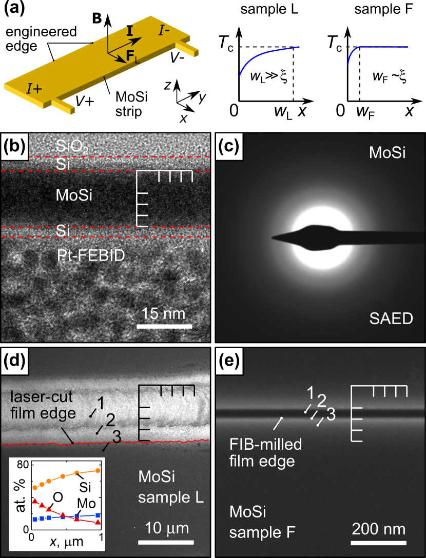
For electrical resistance measurements the films were patterned into a four-probe geometry, with a strip length m and width m. One strip was etched out by laser beam (sample L) and another strip by Ga FIB milling (sample F). The use of different patterning techniques allowed for the realization of rough and smooth edges, respectively, see also Fig. 1(d) and (e).
Laser etching was done under ambient conditions using an LGI-505 gas laser source, with nm wavelength, ns pulse duration and up to 1000 pulses per second of the laser. The beam power, focal spot size and speed of the beam rastering are decisive for the edge quality. These parameters were adjusted to produce an edge shown in Fig. 1(d). The discrete spatial character of the laser beam impact is seen as a circle-footprint contrast variation along the groove etched in the substrate (region 1 in Fig. 1(d)). Gaussian flanks of the laser beam, with a focal spot diameter of about m, caused evaporation of the MoSi film within a region of width -m along the edge (region 2). As a result, an irregular, saw-tooth-like strip edge profile (red thin line in Fig. 1(d)) was created in sample L, characterized by an irregular variation of the edge barrier for vortex entry into the interior of the strip (region 3). The variation of the composition of sample L induced by the laser etching process within a region of width m along the edge, is shown in the inset in Fig. 1(d). The local film composition was inferred from EDX spectroscopy at kV/ nA for a series of nm2 areas probed at different distances from the strip edge. The larger oxygen content in the close-to-edge region leads to a degradation of the superconducting properties. The larger relative contents of Si and O with respect to the Mo70Si30 composition are because of the significantly larger thickness (of about nm) of the layer probed by kV electrons than the film thickness.
FIB milling was done in a dual-beam scanning electron microscope (SEM: FEI Nova NanoLab 600) at 30 kV/30 pA and 20 nm pitch. The milling of a groove (region 1 in Fig. 1(e)) was accompanied by stopping of Ga ions within a region of width nm along the edges in sample F, as inferred from SRIM simulations and seen as a lighter region 2 in the SEM image in Fig. 1(e). The rms edge roughness in the -direction is less than nm, as deduced from an AFM scan over a distance of nm along the edge. Thus, the edges of sample F produce a close-to-perfect edge barrier for vortex entry into the strip (region 3).
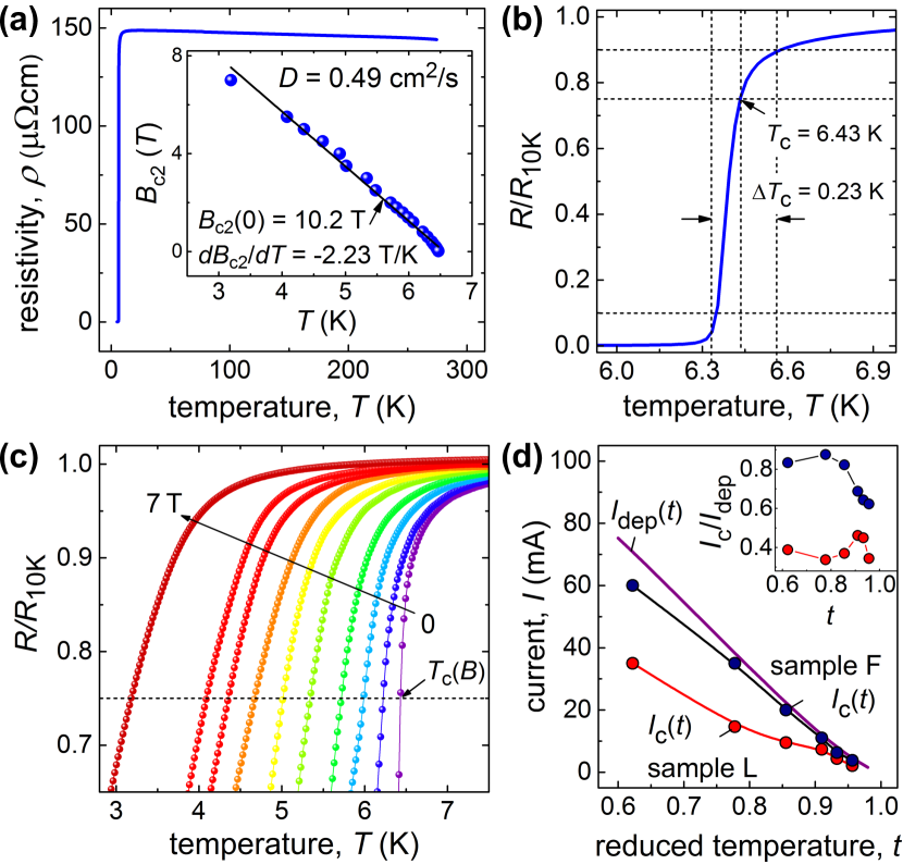
Electrical resistance measurements were done in a He bath cryostat equipped with a superconducting solenoid. Magnetic field was applied perpendicular to the strip plane and the current-voltage (-) curves were recorded in the current-driven regime. The temperature dependence of the resistance exhibits a weak localization behavior (see Fig. 2(a) which is representative for both samples), with a resistivity of cm at K. Figure 2(b) depicts the superconducting transition of the MoSi film at K, as determined by using the % resistance criterion, and the superconducting transition width K, determined as the temperature interval between the % and % of the resistance at K. Application of a magnetic field leads to a broadening of the transition, accompanied with its systematic shift toward lower temperatures, see Fig. 2(c). Near , the temperature dependence of the upper critical field exhibits a slope T/K, whose extrapolation toward zero temperature yields T, see the inset in Fig. 2(a). This slope corresponds to an electron diffusion coefficient of cm2/s, as deduced from the relation Semenov et al. (2009). The coherence length and the penetration depth at zero temperature are estimated Korneeva et al. (2018) as nm and nm, with the Pearl length m. Thus, our strips are thin and wide, with and .
III Results and Discussion
III.1 Critical current and current-voltage curves
The maximal value of the dissipation-free current the superconductor can carry is of primary importance for both, its use in single-photon detectors and the realization of ultra-fast vortex motion. Theoretically, at zero magnetic field, this current is given by the pair-breaking current , whose temperature dependence can be described by the expression
| (1) |
for dirty superconductors Romijn et al. (1982); Clem and Kogan (2012); Korneeva et al. (2018). In Eq. (1), is the superconducting gap at zero temperature, the electron charge, and the sheet resistance. The factor , which is absent for narrow strips (), takes into account the nonuniform current distribution in strips with Plourde et al. (2001). With the BCS ratio we obtain mA for our MoSi strips.
The theoretical dependence calculated by Eq. (1) is compared with the experimentally measured in Fig. 2(d). We used the mV voltage criterion for the deduction of the critical current from the - curves, as illustrated in Fig. 3. This criterion corresponds to the lowest voltage at the foot of the zero-field resistance jump for sample F. Note that in the investigated temperature range , where is the reduced temperature, varies between and for sample L and it is between and for sample F, see the inset in Fig. 2(d).
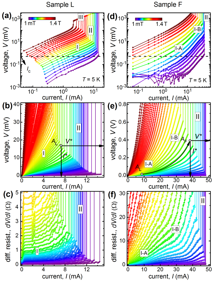
The - curves for both samples are presented in Fig. 3 for K (). In panels (a) and (d) of Fig. 3 we label three distinct regimes in the - curves: (I) the flux-flow regime, (II) the FFI, and (III) the normal conducting regime. Panels (b) and (e) of Fig. 3 show in more detail the nonlinear conductivity regimes preceding the voltage jumps. The last points (A) before the jumps correspond to the instability current related to the instability voltage .
A comparison of the - curves for both samples suggests that sample L transits into the highly-resistive state at noticeably smaller currents than sample F. Herewith, nonlinear upturns in the - curves at the foot of the instability jump occur in a broader range of currents for sample F. This behavior is illustrated by the evolution of the instability point for sample L to the instability point for sample F for the - curves taken at the same field of mT in panels (b) and (e). The extended regime of nonlinear conductivity (I-B) for sample F is also seen in the versus representation in Fig. 3(c) and (f), as compared to the regime of almost linear conductivity (regime I for sample L and regime I-A for sample F) at smaller currents. In this way, at a given magnetic field magnitude, sample F exhibits larger than sample L. This enhancement is most pronounced at low magnetic fields.
III.2 Field dependence of the critical current
Magnetic-field dependence of the critical current allows for the identification of various states the superconductor is passing with increase of the magnetic field Plourde et al. (2001); Ilin et al. (2014); Dobrovolskiy et al. (2020a). Namely, at low magnetic fields the sample can be in the vortex-free (Meissner) state, resulting in a linear decrease of . At higher fields, the decrease slows down, with a crossover at demarcating a transition to the mixed state Maksimova (1998). In the Meissner state (),
| (2) |
contains the factor because of the width . Equation (2) allows us to estimate as mT for sample F. The physical meaning of is the field value at which the surface barrier for vortex entry is suppressed at . The magnetic field dependence of the critical current for both samples is presented in Fig. 4(a). One can see that for sample F the theoretically calculated mT is not very far from the experimental mT and that the very steep decrease of for sample F at (see the inset in Fig. 4(a)) could be an indication for a vortex-free state. Furthermore, the value of for sample F is a factor of 3 larger than for sample L, attesting to strong edge-barrier effects. For 1 mT mT, for sample F is described well by the dependence , indicating the dominating role of the edge barrier for vortex entry in sample F at mT. In general, one could expect a slowing down towards the dependence in larger fields Dobrovolskiy et al. (2020a) because of the transition to the regime of dominating intrinsic (volume) pinning. Indeed, such a transition occurs at larger fields ( mT, not shown) in sample F, pointing to the very small contribution of bulk pinning. This finding is in line with the high structural homogeneity of the amorphous MoSi films (see also Fig. 1(b) and (c)).
By contrast, in sample L, the dependence is flattened at mT. This behavior cannot be explained by a reduction of the edge barrier since the edge roughness leads only to a decrease of and but not to the change of the functional dependence . We believe that this behavior is connected with the change of the structure of MoSi by the laser-beam impact, within a distance of about m from the edge, leading to a strong inhomogeneity of MoSi near the edge and the appearance of vortex pinning there. Some indication for the vortex pinning comes not only from the drastically different dependence of in sample L in comparison with sample F, but also from the comparison of their - curves. Namely, Fig. 3(a) reveals an exponential shape of the - curves which could be considered as an indication of the vortex creep in the near-edge region of sample L.
III.3 Maximal vortex velocity
The magnetic field dependence of the maximal vortex velocity , deduced by using the standard relation , is presented in Fig. 4(b). For both samples decreases with increase of , roughly following the law. However, the values differ substantially, with for sample F being a factor of larger than for sample L in the whole range of magnetic fields. For instance, for sample F, reaches km/s at mT, decreases to km/s at mT, and then slowly decreases to km/s at T. At the same time, for sample L, m/s at mT, decreases to m/s at mT and remains nearly constant with a further increase of the magnetic field.
According to LO, the instability velocity is independent of the magnetic field. As was argued by Doettinger et al Doettinger et al. (1995), the discrepancy between the field-dependent experimental and the field-independent theoretical can be overcome by taking into account the magnetic field dependence of the vortex lattice parameter. Namely, the non-equilibrium electron distribution is spatially uniform only whilst is larger than the intervortex distance . This regime is realized at high magnetic fields, as is also in line with our data in Fig. 4(b), where an almost constant is observed at mT. At smaller fields the system can be recovered to a spatially homogeneous state by allowing to grow accordingly to the increase of with decrease of the applied magnetic field, , where is the magnetic flux quantum. The LO expression is then complemented Doettinger et al. (1995) with the term , yielding
| (3) |
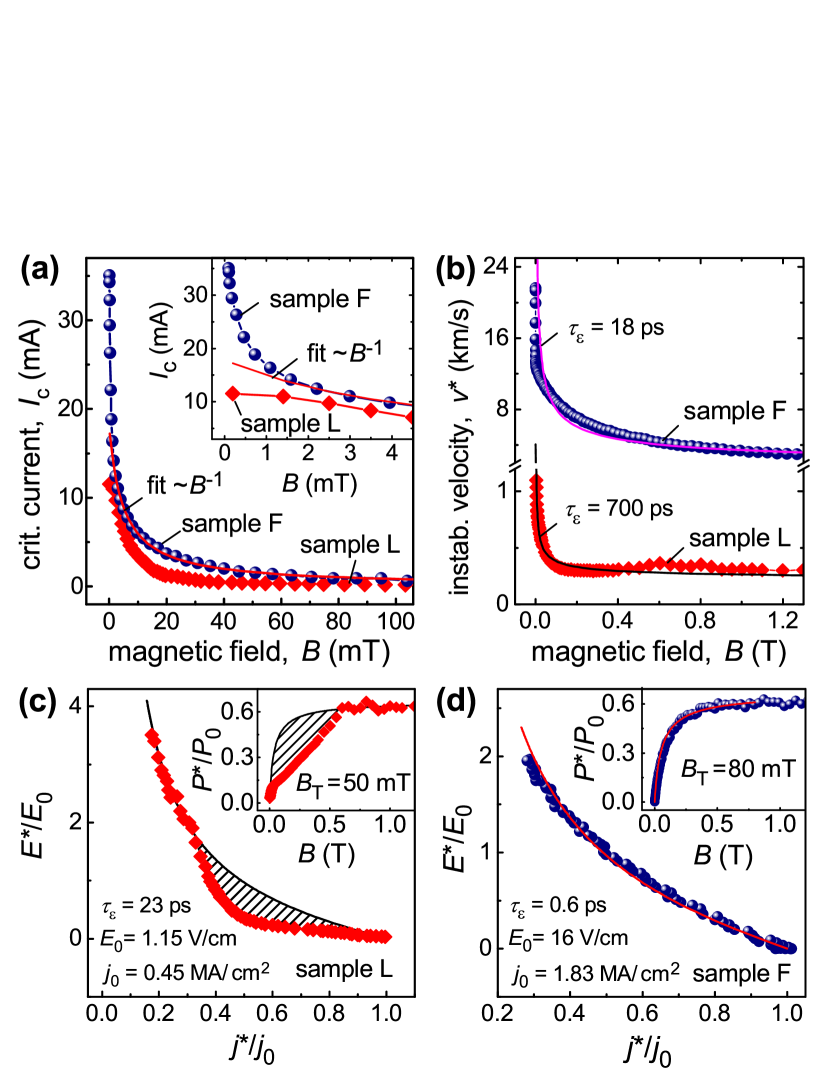
The fits of our experimental data to Eq. (3) are shown by solid lines in Fig. 4(b). Herewith, is calculated while varying the energy relaxation time as the only fitting parameter. Specifically, the fits shown in Fig. 4(b) were obtained with ps and ps for sample L and sample F, respectively. The ratio illustrates that the fits by Eq. (3), which is widely used in recent works Liu et al. (2021); Hofer and Haberkorn (2021), yield differing by more than an order of magnitude for strips made from the same material, but differing by the edge quality.
III.4 Larkin-Ovchinnikov-Bezuglyj-Shklovskij (LOBS) model
The LO theory was generalized by Bezuglyj and Shklovskij (BS) Bezuglyj and Shklovskij (1992) for a finite rate of heat removal from the superconductor to the substrate. Based on the heat balance equation, BS introduced a new field parameter, the overheating field
| (4) |
where is the Boltzmann constant and the heat removal coefficient. The parameter separates the region of small fields at which heat removal is fast enough and the instability is of non-thermal nature from the region of large fields with insufficient heat removal and the heating mechanism dominating the instability. BS derived a scaling law for the electric field strength and the current density at the instability point
| (5) |
where , and are defined as
| (6) |
with the reduced magnetic field and the normal state conductivity . If one fits the entirety of the experimentally deduced instability points to Eq. (6), then the field dependence of the power density at the instability point, allows one to deduce the overheating field and the heat removal coefficient . Substitution of and into Eq. (4) yields then the relaxation time .
The best fits of the experimental data to Eq. (6) for both samples are presented in Fig. 4(c) and (d). For sample L the fit is very poor since in the range of currents the experimental data strongly deviate below the curve calculated by Eq. (6), see the hatched area in Fig. 4(c). The fit in Fig. 4(c) was done with V/cm and MA/cm2, yielding mT, W/Kcm2, and ps. For sample F the fit is almost perfect as the experimental data fall onto the curve calculated by Eq. (6) in the entire range of magnetic fields. The fit in Fig. 4(d) was done with V/cm and MA/cm2, yielding mT, W/Kcm2, and ps. If one associates with the electron-phonon scattering time in the LO model Larkin and Ovchinnikov (1986), the deduced is at least one order of magnitude smaller than one could expect from found in similar low- highly disordered superconductors Babic et al. (2004); Sidorova et al. (2018, 2020). We note that the LO theory was developed neglecting the diffusion term in the kinetic equation. This approximation is justified when the intervortex distance is smaller than the quasiparticles diffusion length , with nm and nm suggesting that the deduced values can hardly be treated even as order-of-magnitude estimates. Nonetheless, while the values of deduced from the LOBS model Bezuglyj and Shklovskij (1992) differ from those deduced from the model of Doettinger et al Doettinger et al. (1995), the ratio between the deduced relaxation times is almost the same, .
III.5 Numerical modeling
To get further insights into the spatiotemporal evolution of the order parameter in the strips with and without edge defects, we numerically solve the modified TDGL equation in conjunction with the heat balance equation. The essential equations and the considered boundary conditions are detailed in Appendix A.
The shapes of the edges of sample L are unknown and their exact modeling is not feasible with the currently available computation capabilities. Therefore we consider the effects of single edge defects of different shapes and an array of defects located near the edge of the strip. The defects are simulated as regions with a locally suppressed critical temperature.
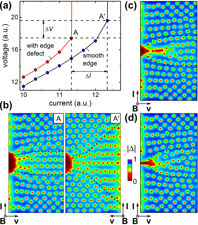
The results of TDGL simulations for a single defect are presented in Fig. 5. Figure 5(a) presents the - curves calculated for the vortex entry through the edge containing a single, semicircle-shaped edge defect in comparison with the - curve for the vortex entry through the perfectly straight edge of the same strip. The simulations suggest that the low-dissipative regime of nonlinear conductivity extends toward larger currents (and, hence, higher vortex velocities) for the vortex entry via the perfect edge (point A′ Fig. 5(a)). The spatial dependences of the superconducting order parameter at the last points before the instability jumps are illustrated in Fig. 5(b). Panel A in Fig. 5(b) illustrates the case when vortices enter via the edge containing a semicircle-shaped defect, while panel A′ illustrates the case when they enter via the opposite smooth edge. The influence of the edge defect on the vortex dynamics is twofold. First, due to the current-crowding effect the defect suppresses the edge barrier for the penetration of vortices, turning the defect into the place of nucleation of vortex rivers Vodolazov (2019). Such vortex rivers represent self-organized Josephson-like junctions formed by chains of fast-moving vortices, which eventually evolve to normal domains expanding across the entire sample upon its abrupt transition to the highly-resistive state. Second, the local deflection of the current flow direction from the axis (see Fig. 1(a)) near the defect leads to the deviation of the Lorentz force direction and, hence, the direction of vortex motion from the axis. As a result, a diverging “jet” of vortices is formed, as indicated by the dashed lines in panel A in Fig. 5(b).
By contrast, when vortices enter via the perfect edge (panel A′ in Fig. 5(b)), the only effect which remains in comparison with the previously considered case is the local enhancement of the current density near the edge defect. Panel A′ in Fig. 5(b) shows that the nucleation of vortex rivers occurs at many different points along the perfect edge, while only those nucleated at the edge in front of the defect develop faster because of the larger current density. Figure 5(c) and (d) illustrate the development of vortex “jets” upon vortex entry via the edge containing a triangle-shaped and a slit-shaped defect.
The simulations also allow us to explain the role of a single defect on the FFI observed in Ref. Dobrovolskiy et al. (2020a). As in that experiment, our model gives a several-percent suppression of and when vortices enter via an edge of the strip containing a defect compared to entry through the smooth edge, while can be suppressed by more than two times (depending on the size and shape of the defect). That experimental observation Dobrovolskiy et al. (2020a) follows from the considered model, where FFI starts near the edge because of the higher local current density and the electronic temperature , but in the rest of the strip the vortices have to move at a large enough velocity to allow for the appearance of vortex rivers Silhanek et al. (2010). Thus, the edge defect increases and in comparison with the strip with the smooth edge and it leads to smaller and , but their values do not change drastically since the change in the current distribution decays fast with increase of the distance from the defect (approximately inversely proportional to the square of the distance).
In our experiment, the difference in and for samples L and F is several times larger. In comparison with Ref. Dobrovolskiy et al. (2020a) in our case the laser etching not only creates edge defects but it also changes the material composition of the close-to-edge regions. To take this into account in the simulations, we introduced randomly distributed defects (each defect has a size of with a locally suppressed ) in the close-to-edge region of width for the strip with . However, the results for this system are similar to the ones for the strip with a single edge defect, namely, a relatively small suppression of and while the critical current could be suppressed significantly (as in the case of a single defect).
A comparison of the experimental results for samples L and F implies that FFI appears first in the close-to-edge region of sample L with width m m (which is inhomogeneous due to the laser etching) and only then the FFI spreads to the rest of the superconducting strip. Unfortunately, our model does not describe this process. We also tried to simulate the initial FFI by introducing a local increase of the escape time of nonequilibrium phonons to the substrate in the close-to-edge region. Specifically, was larger by an order of magnitude in the region with width for a strip with . Indeed, we have found that in that region FFI sets on first but it does not spread deep into the strip, because of the cooling of the close-to-edge regions via diffusion of hot electrons to the neighboring regions. We have to note that the so-called healing length at the chosen parameters in our simulations is much larger than the length of penetration of the electric field. Whether it plays an important role or does not for spreading of the normal region into the interior of the strip should be clarified in further investigations.
IV Conclusion
To sum up, we have investigated the effects of edge quality on the critical current and maximal vortex velocities in wide thin films of MoSi. The edges of different quality were produced by laser etching (sample L) and milling by a focused ion beam (sample F). The smooth edges in sample F have allowed for (i) a factor of about 3 increase of the zero-field critical current, (ii) a factor of 20 enhancement of the maximal vortex velocity up to about 20 km/s, and (iii) a factor of 40 smaller estimate for the energy relaxation time on the 20 ps time scale.
Our results have following implications for superconducting devices. First, the enhancement of the current-carrying capability of the strips is relevant for superconductor microstrip single-photon detectors (SMSPDs). Namely, to achieve the theoretically predicted intrinsic detection efficiency of about 100%, SMSPDs should be biased by close-to-deparing critical currents Vodolazov (2017). In particular, in the MoSi strips with FIB-milled edges at 5 K the zero field critical current has increased by a factor of 3, reaching 87% of the Ginzburg-Landau pair-breaking current. Second, the improvement of the current-carrying capability has allowed for the enhancement of the maximal vortex velocity, providing access to the previously inaccessible regimes (in this material) of generation of sound and spin waves via a Cherenkov-type mechanism Bulaevskii and Chudnovsky (2005); Bespalov et al. (2014); Dobrovolskiy et al. (2021), with a rich physics of fluxon-phonon and fluxon-magnon interactions Ivlev et al. (1999); Dobrovolskiy et al. (2019b). From the viewpoint of basic research, our findings could be relevant for a possible explanation of the inconsistency between the (sub-)ns relaxation times deduced from current-voltage measurements for many dirty superconductors, despite their potential (or already proven) capability of single-photon counting Liu et al. (2021); Samoilov et al. (1995); Doettinger et al. (1997); Hofer and Haberkorn (2021); Cirillo et al. (2021); Lin et al. (2013).
In all, our findings suggest the edge quality check as a route to improvement of the critical current in superconducting microstrip single-photon detectors and imply that homogeneous, dirty-limit superconductors with weak pinning should generally allow for ultra-fast vortex motion at velocities exceeding km/s. In particular, our results imply that for strips where no care was taken about the edge quality and the magnetic field dependence of the critical current does not attest to the dominating edge pinning of vortices, the flux-flow instability only allows for the deduction of some “indicative” relaxation time exceeding the intrinsic in the material.
Appendix A
Simulation results presented in Fig. 5 rely upon the solution of the modified TDGL equation Vodolazov (2017)
where , is the vector potential, the electrostatic potential, the diffusion coefficient, , the normal-state conductivity, the single-spin density of states at the Fermi level, and and are the superconducting current densities in the Usadel and Ginzburg-Landau models
where , is the phase of , and
At not very close to the Ginzburg-Landau expression for the superconducting current is not valid quantitatively and one needs to use the Usadel expression for . In this case the TDGL equation should also be modified since the ordinary TDGL equation leads to in the stationary case, while one needs . Accordingly, by adding the term in the TDGL equation one provides . At the modified TDGL equation reduces to the ordinary TDGL equation and goes to zero.
The electron and phonon temperatures, and , respectively, are found from the solution of following equations
where , is the change in the energy of electrons due to the transition to the superconducting state, is the heat conductivity in the superconducting state
is the heat conductivity in the normal state, the term describes Joule dissipation, and is the escape time of nonequilibrium phonons to the substrate. The parameter is defined as , where and are the heat capacities of electrons and phonons at , and the characteristic time controls the strength of the electron-phonon and phonon-electron scattering Vodolazov (2017). Values of the parameters and ns used in the calculations are estimates for NbN. Their variation only leads to quantitative changes in the - curves.
The current continuity equation is solved to find the electrostatic potential. Here, is the normal current density. At the edges where vortices enter and exit the microstrip we use the boundary conditions and , while at the edges along the current direction , , , . The latter boundary conditions model the contact of the superconducting strip with a normal reservoir being in equilibrium. This choice provides a way “to inject” the current into the superconducting microstrip in the modeling. The modeled length of the microstrip is .
Acknowledgements.
The authors thank Roland Sachser for support with the nanofabrication. B.B. acknowledges financial support by the Vienna Doctoral School in Physics (VDSP). D.Y.V. acknowledges support by the Russian Foundation for Basic Research (RFBR), grant No. 18-29-20100. Support through the Frankfurt Center of Electron Microscopy (FCEM), by the Austrian Science Fund (FWF) grant No. I4865N and by the European Cooperation in Science and Technology via COST Actions CA16218 (NANOCOHYBRI) and CA19108 (HiSCALE) is gratefully acknowledged.References
- Embon et al. (2017) L. Embon, Y. Anahory, Z. L. Jelic, E. O. Lachman, Y. Myasoedov, M. E. Huber, G. P. Mikitik, A. V. Silhanek, M. V. Milosevic, A. Gurevich, and E. Zeldov, “Imaging of super-fast dynamics and flow instabilities of superconducting vortices,” Nat. Commun. 8, 85 (2017).
- Rouco et al. (2018) V. Rouco, M. Massarotti, D. Stornaiuolo, G. P. Papari, X. Obradors, T. Puig, F. Tafuri, and A. Palau, “Vortex lattice instabilities in YBa2Cu3O7-x nanowires,” Materials 11, 211 (2018).
- Dobrovolskiy et al. (2019a) O. V. Dobrovolskiy, V. M. Bevz, E. Begun, R. Sachser, R. V. Vovk, and M. Huth, “Fast dynamics of guided magnetic flux quanta,” Phys. Rev. Appl. 11, 054064 (2019a).
- Leo et al. (2020) A. Leo, A. Nigro, V. Braccini, G. Sylva, A. Provino, A. Galluzzi, M. Polichetti, C. Ferdeghini, M. Putti, and G. Grimaldi, “Flux flow instability as a probe for quasiparticle energy relaxation time in Fe-chalcogenides,” Supercond. Sci. Technol. 33, 104005 (2020).
- Dobrovolskiy et al. (2020a) O. V. Dobrovolskiy, D. Yu Vodolazov, F. Porrati, R. Sachser, V. M. Bevz, M. Yu Mikhailov, A. V. Chumak, and M. Huth, “Ultra-fast vortex motion in a direct-write Nb-C superconductor,” Nat. Commun. 11, 3291 (2020a).
- Ustavschikov et al. (2020) S. S. Ustavschikov, M. Yu. Levichev, I. Yu. Pashenkin, A. M. Klushin, and D. Yu. Vodolazov, “Approaching depairing current in dirty thin superconducting strip covered by low resistive normal metal,” Supercond. Sci. Technol. 34, 015004 (2020).
- Vodolazov (2019) D. Yu. Vodolazov, “Flux-flow instability in a strongly disordered superconducting strip with an edge barrier for vortex entry,” Supercond. Sci. Technol. 32, 115013 (2019).
- Bezuglyj et al. (2019) Alexei I. Bezuglyj, Valerij A. Shklovskij, Ruslan V. Vovk, Volodymyr M. Bevz, Michael Huth, and Oleksandr V. Dobrovolskiy, “Local flux-flow instability in superconducting films near ,” Phys. Rev. B 99, 174518 (2019).
- Kogan and Prozorov (2020) V. G. Kogan and R. Prozorov, “Interaction between moving Abrikosov vortices in type-II superconductors,” Phys. Rev. B 102, 024506 (2020).
- Pathirana and Gurevich (2020) W. P. M. R. Pathirana and A. Gurevich, “Nonlinear dynamics and dissipation of a curvilinear vortex driven by a strong time-dependent Meissner current,” Phys. Rev. B 101, 064504 (2020).
- Kogan and Nakagawa (2021) V. G. Kogan and N. Nakagawa, “Current distributions by moving vortices in superconductors,” Phys. Rev. B 103, 134511 (2021).
- Pathirana and Gurevich (2021) W. P. M. R. Pathirana and A. Gurevich, “Effect of random pinning on nonlinear dynamics and dissipation of a vortex driven by a strong microwave current,” Phys. Rev. B 103, 184518 (2021).
- Ivlev et al. (1999) B. I. Ivlev, S. Mejía-Rosales, and M. N. Kunchur, “Cherenkov resonances in vortex dissipation in superconductors,” Phys. Rev. B 60, 12419–12423 (1999).
- Bulaevskii and Chudnovsky (2005) L. N. Bulaevskii and E. M. Chudnovsky, “Sound generation by the vortex flow in type-II superconductors,” Phys. Rev. B 72, 094518 (2005).
- Bespalov et al. (2014) A. A. Bespalov, A. S. Mel’nikov, and A. I. Buzdin, “Magnon radiation by moving Abrikosov vortices in ferromagnetic superconductors and superconductor-ferromagnet multilayers,” Phys. Rev. B 89, 054516 (2014).
- Dobrovolskiy et al. (2021) O. V. Dobrovolskiy, Q. Wang, D. Yu. Vodolazov, B. Budinska, R. Sachser, A.V. Chumak, M. Huth, and A. I. Buzdin, “Cherenkov radiation of spin waves by ultra-fast moving magnetic flux quanta,” arXiv:2103.10156 (2021).
- Korneeva et al. (2018) Yu. P. Korneeva, D. Yu. Vodolazov, A. V. Semenov, I. N. Florya, N. Simonov, E. Baeva, A. A. Korneev, G. N. Goltsman, and T. M. Klapwijk, “Optical single-photon detection in micrometer-scale NbN bridges,” Phys. Rev. Appl. 9, 064037 (2018).
- Korneeva et al. (2020) Yu. P. Korneeva, N.N. Manova, I.N. Florya, M. Yu. Mikhailov, O.V. Dobrovolskiy, A.A. Korneev, and D. Yu. Vodolazov, “Different single-photon response of wide and narrow superconducting strips,” Phys. Rev. Appl. 13, 024011 (2020).
- Charaev et al. (2020) I. Charaev, Y. Morimoto, A. Dane, A. Agarwal, M. Colangelo, and K. K. Berggren, “Large-area microwire MoSi single-photon detectors at 1550 nm wavelength,” Appl. Phys. Lett. 116, 242603 (2020).
- Chiles et al. (2020) J. Chiles, S. M. Buckley, A. Lita, V. B. Verma, J. Allmaras, B. Korzh, M. D. Shaw, J. M. Shainline, R. P. Mirin, and S. W. Nam, “Superconducting microwire detectors based on WSi with single-photon sensitivity in the near-infrared,” Appl. Phys. Lett. 116, 242602 (2020).
- Vodolazov (2017) D. Yu. Vodolazov, “Single-photon detection by a dirty current-carrying superconducting strip based on the kinetic-equation approach,” Phys. Rev. Appl. 7, 034014 (2017).
- Caputo et al. (2017) M. Caputo, C. Cirillo, and C. Attanasio, “NbRe as candidate material for fast single photon detection,” Appl. Phys. Lett. 111, 192601 (2017).
- Hofer and Haberkorn (2021) J. A. Hofer and N. Haberkorn, “Flux flow velocity instability and quasiparticle relaxation time in nanocrystalline -W thin films,” Thin Sol. Films 730, 138690 (2021).
- Liu et al. (2021) Z. Liu, B. Luo, L. Zhang, B. Hou, and D. Wang, “Vortex dynamics in amorphous MoSi superconducting thin films,” Supercond. Sci. Technol. (2021).
- Cirillo et al. (2021) C. Cirillo, V. Granata, A. Spuri, A. Di Bernardo, and C. Attanasio, “NbReN: A disordered superconductor in thin film form for potential application as superconducting nanowire single photon detector,” Phys. Rev. Mater. 5, 085004 (2021).
- Larkin and Ovchinnikov (1975) A. I. Larkin and Yu. N. Ovchinnikov, “Nonlinear conductivity of superconductors in the mixed state,” J. Exp. Theor. Phys. 41, 960 (1975).
- Larkin and Ovchinnikov (1986) A. I. Larkin and Y. N. Ovchinnikov, “Nonequilibrium superconductivity,” (Elsevier, Amsterdam, 1986) p. 493.
- Bezuglyj and Shklovskij (1992) A.I. Bezuglyj and V.A. Shklovskij, “Effect of self-heating on flux flow instability in a superconductor near ,” Physica C 202, 234 (1992).
- Silhanek et al. (2012) A. V. Silhanek, A. Leo, G. Grimaldi, G. R. Berdiyorov, M. V Milosevic, A. Nigro, S. Pace, N. Verellen, W. Gillijns, V. Metlushko, B. Ilić, X. Zhu, and V. V. Moshchalkov, “Influence of artificial pinning on vortex lattice instability in superconducting films,” New J. Phys. 14, 053006 (2012).
- Shklovskij et al. (2017) V. A. Shklovskij, A. P. Nazipova, and O. V. Dobrovolskiy, “Pinning effects on self-heating and flux-flow instability in superconducting films near ,” Phys. Rev. B 95, 184517 (2017).
- Dobrovolskiy et al. (2017) O. V. Dobrovolskiy, V. A. Shklovskij, M. Hanefeld, M. Zörb, L. Köhs, and M. Huth, “Pinning effects on flux flow instability in epitaxial Nb thin films,” Supercond. Sci. Technol. 30, 085002 (2017).
- Dobrovolskiy et al. (2020b) O. V. Dobrovolskiy, C. González-Ruano, A. Lara, R. Sachser, V. M. Bevz, V. A. Shklovskij, A. I. Bezuglyj, R. V. Vovk, M. Huth, and F. G. Aliev, “Moving flux quanta cool superconductors by a microwave breath,” Commun. Phys. 3, 64 (2020b).
- Watts-Tobin et al. (1981) R. J. Watts-Tobin, Y. Krähenbühl, and L. Kramer, “Nonequilibrium theory of dirty, current-carrying superconductors: phase-slip oscillators in narrow filaments near Tc,” J. Low Temp. Phys. 42, 459–501 (1981).
- Korzh et al. (2020) B. Korzh, Q.-Y. Zhao, J. P. Allmaras, S. Frasca, T. M. Autry, E. A. Bersin, A. D. Beyer, R. M. Briggs, B. Bumble, M. Colangelo, G. M. Crouch, A. E. Dane, T. Gerrits, A. E. Lita, F. Marsili, G. Moody, C. Peña, E. Ramirez, J. D. Rezac, N. Sinclair, M. J. Stevens, A. E. Velasco, V. B. Verma, E. E. Wollman, S. Xie, D. Zhu, P. D. Hale, M. Spiropulu, K. L. Silverman, R. P. Mirin, S. W. Nam, A. G. Kozorezov, M. D. Shaw, and K. K. Berggren, “Demonstration of sub-3 ps temporal resolution with a superconducting nanowire single-photon detector,” Nat. Photon. 14, 250–255 (2020).
- Cirillo et al. (2020) C. Cirillo, J. Chang, M. Caputo, J. W. N. Los, S. Dorenbos, I. Esmaeil Zadeh, and C. Attanasio, “Superconducting nanowire single photon detectors based on disordered NbRe films,” Appl. Phys. Lett. 117, 172602 (2020).
- Samoilov et al. (1995) A. V. Samoilov, M. Konczykowski, N. C. Yeh, S. Berry, and C. C. Tsuei, “Electric-field-induced electronic instability in amorphous Si superconducting films,” Phys. Rev. Lett. 75, 4118–4121 (1995).
- Doettinger et al. (1997) S. G. Doettinger, S. Kittelberger, R. P. Huebener, and C. C. Tsuei, “Quasiparticle energy relaxation in the cuprate superconductors,” Phys. Rev. B 56, 14157–14162 (1997).
- Lin et al. (2013) S.-Z. Lin, O. Ayala-Valenzuela, R. D. McDonald, L. N. Bulaevskii, T. G. Holesinger, F. Ronning, N. R. Weisse-Bernstein, T. L. Williamson, A. H. Mueller, M. A. Hoffbauer, M. W. Rabin, and M. J. Graf, “Characterization of the thin-film NbN superconductor for single-photon detection by transport measurements,” Phys. Rev. B 87, 184507 (2013).
- Gurevich and Mints (1984) A. V. Gurevich and R. G. Mints, Sov. Phys. Usp. 27, 19 (1984).
- Bezuglyj and Shklovskij (1984) A. I. Bezuglyj and V. A. Shklovskij, “Thermal domains in inhomogeneous current-carrying superconductors. current-voltage characteristics and dynamics of domain formation after current jumps,” J. Low Temp. Phys. 57, 227–247 (1984).
- Buzdin and Daumens (1998) A. Buzdin and M. Daumens, “Electromagnetic pinning of vortices on different types of defects,” Physica C 294, 257–269 (1998).
- Aladyshkin et al. (2001) A.Yu. Aladyshkin, A. S. Mel’nikov, I. A. Shereshevsky, and I. D. Tokman, “What is the best gate for vortex entry into type-II superconductor?” Physica C 361, 67–72 (2001).
- Vodolazov et al. (2003) D. Y. Vodolazov, I. L. Maksimov, and E. H. Brandt, “Vortex entry conditions in type-II superconductors: Effect of surface defects,” Physica C 384, 211–226 (2003).
- Clem and Berggren (2011) J. R. Clem and K. K. Berggren, “Geometry-dependent critical currents in superconducting nanocircuits,” Phys. Rev. B 84, 174510 (2011).
- Mikitik (2021) G. P. Mikitik, “Critical current in thin flat superconductors with Bean-Livingston and geometrical barriers,” Phys. Rev. B 104, 094526 (2021).
- Caloz et al. (2018) M. Caloz, M. Perrenoud, C. Autebert, B. Korzh, M. Weiss, Ch. Schönenberger, R. J. Warburton, H. Zbinden, and F. Bussières, “High-detection efficiency and low-timing jitter with amorphous superconducting nanowire single-photon detectors,” Appl. Phys. Lett. 112, 061103 (2018).
- Korneeva et al. (2014) Yu. P. Korneeva, M. Yu. Mikhailov, Yu. P. Pershin, N. N. Manova, A. V. Divochiy, Yu. B. Vakhtomin, A. A. Korneev, K. V. Smirnov, A. G. Sivakov, A. Yu. Devizenko, and G. N. Goltsman, “Superconducting single-photon detector made of MoSi film,” Supercond. Sci. Technol. 27, 095012 (2014).
- Dobrovolskiy et al. (2015) O. V. Dobrovolskiy, M. Kompaniiets, R. Sachser, F. Porrati, Ch. Gspan, H. Plank, and M. Huth, “Tunable magnetism on the lateral mesoscale by post-processing of Co/Pt heterostructures,” Beilstein J. Nanotech. 6, 1082–1090 (2015).
- Porrati et al. (2019) F. Porrati, S. Barth, R. Sachser, O. V. Dobrovolskiy, A. Seybert, A. S. Frangakis, and M. Huth, “Crystalline niobium carbide superconducting nanowires prepared by focused ion beam direct writing,” ACS Nano 13, 6287–6296 (2019).
- Semenov et al. (2009) A. Semenov, B. Günther, U. Böttger, H.-W. Hübers, H. Bartolf, A. Engel, A. Schilling, K. Ilin, M. Siegel, R. Schneider, D. Gerthsen, and N. A. Gippius, “Optical and transport properties of ultrathin nbn films and nanostructures,” Phys. Rev. B 80, 054510 (2009).
- Romijn et al. (1982) J. Romijn, T. M. Klapwijk, M. J. Renne, and J. E. Mooij, “Critical pair-breaking current in superconducting aluminum strips far below ,” Phys. Rev. B 26, 3648–3655 (1982).
- Clem and Kogan (2012) John R. Clem and V. G. Kogan, “Kinetic impedance and depairing in thin and narrow superconducting films,” Phys. Rev. B 86, 174521 (2012).
- Plourde et al. (2001) B. L. T. Plourde, D. J. Van Harlingen, D. Yu. Vodolazov, R. Besseling, M. B. S. Hesselberth, and P. H. Kes, “Influence of edge barriers on vortex dynamics in thin weak-pinning superconducting strips,” Phys. Rev. B 64, 014503 (2001).
- Ilin et al. (2014) K. Ilin, D. Henrich, Y. Luck, Y. Liang, M. Siegel, and D. Yu. Vodolazov, “Critical current of Nb, NbN, and TaN thin-film bridges with and without geometrical nonuniformities in a magnetic field,” Phys. Rev. B 89, 184511 (2014).
- Maksimova (1998) G. M. Maksimova, “Mixed state and critical current in narrow semiconducting films,” Phys. Sol. Stat. 40, 1607–1610 (1998).
- Doettinger et al. (1995) S.G. Doettinger, R.P. Huebener, and A. Kühle, “Electronic instability during vortex motion in cuprate superconductors regime of low and high magnetic fields,” Physica C 251, 285 – 289 (1995).
- Babic et al. (2004) D. Babic, J. Bentner, C. Sürgers, and C. Strunk, “Flux-flow instabilities in amorphous microbridges,” Phys. Rev. B 69, 092510–1–4 (2004).
- Sidorova et al. (2018) Mariia V. Sidorova, A. G. Kozorezov, A. V. Semenov, Yu. P. Korneeva, M. Yu. Mikhailov, A. Yu. Devizenko, A. A. Korneev, G. M. Chulkova, and G. N. Goltsman, “Nonbolometric bottleneck in electron-phonon relaxation in ultrathin WSi films,” Phys. Rev. B 97, 184512 (2018).
- Sidorova et al. (2020) M. Sidorova, A. Semenov, H.-W. Hübers, K. Ilin, M. Siegel, I. Charaev, M. Moshkova, N. Kaurova, G. N. Goltsman, X. Zhang, and A. Schilling, “Electron energy relaxation in disordered superconducting NbN films,” Phys. Rev. B 102, 054501 (2020).
- Silhanek et al. (2010) A. V. Silhanek, M. V. Milošević, R. B. G. Kramer, G. R. Berdiyorov, J. Van de Vondel, R. F. Luccas, T. Puig, F. M. Peeters, and V. V. Moshchalkov, “Formation of stripelike flux patterns obtained by freezing kinematic vortices in a superconducting Pb film,” Phys. Rev. Lett. 104, 017001 (2010).
- Dobrovolskiy et al. (2019b) O. V. Dobrovolskiy, R. Sachser, T. Brächer, T. Böttcher, V. V. Kruglyak, R. V. Vovk, V. A. Shklovskij, M. Huth, B. Hillebrands, and A. V. Chumak, “Magnon-fluxon interaction in a ferromagnet/superconductor heterostructure,” Nat. Phys. 15, 477 (2019b).