Digital control of a superconducting qubit using a Josephson pulse generator at 3 K
Abstract
Scaling of quantum computers to fault-tolerant levels relies critically on the integration of energy-efficient, stable, and reproducible qubit control and readout electronics. In comparison to traditional semiconductor control electronics (TSCE) located at room temperature, the signals generated by Josephson junction (JJ) based rf sources benefit from small device sizes, low power dissipation, intrinsic calibration, superior reproducibility, and insensitivity to ambient fluctuations. Previous experiments to co-locate qubits and JJ-based control electronics resulted in quasiparticle poisoning of the qubit; degrading the qubit’s coherence and lifetime. In this paper, we digitally control a 0.01 K transmon qubit with pulses from a Josephson pulse generator (JPG) located at the 3 K stage of a dilution refrigerator. We directly compare the qubit lifetime , coherence time , and thermal occupation when the qubit is controlled by the JPG circuit versus the TSCE setup. We find agreement to within the daily fluctuations on s and s for and , respectively, and agreement to within the 1% error for . Additionally, we perform randomized benchmarking to measure an average JPG gate error of . In combination with a small device size ( mm2) and low on-chip power dissipation (W), these results are an important step towards demonstrating the viability of using JJ-based control electronics located at temperature stages higher than the mixing chamber stage in highly-scaled superconducting quantum information systems.
I Introduction
Error-corrected quantum computers are projected to require large numbers, , of qubits [1, 2, 3, 4]; placing stringent requirements on the per-qubit hardware overhead. Superconducting quantum circuits are a leading technology for scaling existing systems into the noisy intermediate-scale quantum (NISQ) era of qubits. In present systems, qubit gates and entangling operations are performed using shaped microwave pulses synthesized using instrumentation at room temperature [5] – here referred to as traditional semiconductor control electronics (TSCE). Signals are routed into a dilution refrigerator (DR) to the K qubits and typically attenuated by 40–60 dB to suppress thermal noise on drive lines [6].
Limitations in cryogenic cooling power, TSCE power instability [7], and system complexity mandate a shift to miniaturize and enhance the stability/precision of waveform generation in superconducting quantum information systems. Recently, the pulse-shaping DAC/mixers used to generate qubit control signals have been successfully integrated at 3 K [8, 9] and 100 mK [10] using cryogenic CMOS (cryoCMOS) technology. While an impressive step towards miniaturization and large-scale integration, a significant gap exists between these devices and scalable qubit control. Specifically, gate fidelity; power dissipation; and the accuracy, stability, and repeatability of the signals need improvement [11, 7, 12].
The scalability constraints of physical size and power consumption per channel may be satisfied by superconducting Josephson junction (JJ) signal generator circuits or aforementioned cryoCMOS controllers. Comparable to cryoCMOS devices, JJ circuits have small device sizes ( cm2) and very low on-chip power dissipation (W); while also leveraging the intrinsically-calibrated nature of single flux quantum (SFQ) pulses. This feature provides avenues for improving waveform quality and repeatability beyond what is achievable using semiconductor-based generators. Capitalizing on pulse area quantization enables use of JJ arrays to construct exceptionally stable and repeatable voltage sources from dc to a few gigahertz [13, 14, 15, 16]. Similar devices are used to realize intrinsically accurate voltages for the international system of units, and are disseminated worldwide as primary dc and ac voltage standards [17]. Furthermore, the use of SFQ pulses has been proposed as a scalable paradigm for digitally controlling qubits [18, 19, 20], and was recently demonstrated with a SFQ driver and qubit circuit co-fabricated on the same chip [21].
The primary limitation of SFQ operation proximal to quantum arrays is degradation of qubit lifetimes from quasiparticles created during pulse generation [22, 23]. A solution that mitigates these quasiparticles must be implemented – such as physically separating the SFQ elements and qubits. In this work we locate the JJ control circuitry on the 3 K DR stage to interrupt quasiparticle-qubit propagation. Similar to [21], we deliver sparse trains of pulses subresonantly to enact control – giving our device its name of the Josephson pulse generator (JPG). A 0.01 K bump-bonded multi-chip configuration [24, 25] and/or introduction of normal-metal quasiparticle traps can also be effective for quasiparticle mitigation [26, 27].
Location of the cryogenic control electronics at a higher temperature stage liberates physical volume at 0.01 K – commonly monopolized by the quantum array and readout hardware – and leverages higher cooling powers. This approach may also benefit from integration with cryoCMOS circuits by exploiting the advantages of cryoCMOS-implemented logic/memory elements [9, 8, 10]. Location of the control electronics at 3 K does increase wiring complexity and the parasitic heat loads to the K stages; however, solutions are under development which demonstrate low thermal loading and crosstalk [28, 29, 30].
While the aforementioned merits of JJ-based sources [17] are expected to apply for qubit control, this work is the first validation of using JJ-based pulse generation at 3 K to control a 0.01 K qubit. Here we show that the JPG does not adversely affect the qubit by separately measuring the qubit energy relaxation time , coherence time , and thermal occupancy with both a TSCE setup and the JPG. Our findings show good agreement in all three metrics with each control setup. Additionally, we measure the JPG gate fidelity to be within an order of magnitude of the qubit coherence limit, and provide discussion of future devices expected to yield coherence-limited gates.
II JPG-based Qubit Control
An input current evolving the JJ superconducting phase difference by generates a voltage pulse whose time-integrated area equals the magnetic flux quantum :
| (1) |
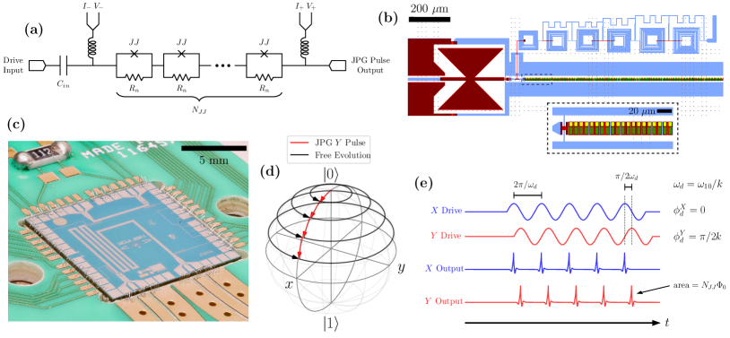
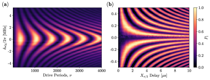
The duration of this SFQ pulse is approximately , where is the JJ characteristic time, is its critical current, and is its normal resistance [31]. SFQ signal amplification can be achieved by connecting a series of junctions whose pulses add coherently. This yields a larger pulse of area , which we call a JPG pulse. Depending on qubit coupling to the control line, arrays with are required if located at 3 K. In this work our JPG has , mA, and m – resulting in a characteristic frequency of GHz. Fig. 1(a)–(c) show a schematic, portion of the JPG layout, and image of the packaged device.
If is much larger than the qubit transition frequency, , then during pulse arrival the qubit undergoes a discrete rotation
| (2) |
where is the JPG-qubit amplitude attenuation, is the control line-qubit coupling capacitance, and is the qubit capacitance [18]. , , and may be treated as free design parameters to realize a combination of adequate control line thermalization and tip-angle per pulse, . For 3D readout cavity configurations also encapsulates attenuation from pulse transit of the cavity resonance. A train of sharp pulses arriving resonantly to the qubit (), or at a subharmonic (, where is an integer), discretely rotate the qubit around the Bloch sphere during pulse arrival, while between pulses the qubit precesses for periods at fixed (see Fig. 1(d)).
In our implementation the JPG must be driven using a sinusoidal signal at because there is no isolation between the drive input and device output. Otherwise, the large drive signal dominates and induces spurious qubit rotations. Generation of an integer number of JPG pulses is performed by sending an integer number of sinusoidal drive periods, . Under the correct bias parameters there is a one-to-one correspondence between the number of JPG pulses generated and the number of drive periods (). Orthogonal axis control, realized by phasing the drive signal relative to a timing reference, is depicted in Fig. 1(e). More details are found in Supplementary Material XI.
III Experimental Details
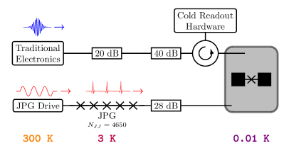
In this work we use a transmon qubit dispersively coupled to a 3D aluminum readout cavity possessing two control lines with different coupling strengths. A simplified experimental schematic is shown in Fig 2. The JPG is connected to the cavity’s weakly-coupled port (0.175 MHz coupling rate) and the TSCE control and readout line to its strongly-coupled port (2.01 MHz coupling rate). With this setup, a direct comparison of qubit performance with both control schemes is possible during the same cooldown. This qubit was measured for a previous publication; for other parameters see [32].
Qubit state readout is performed by probing the qubit-state-dependent frequency shift of the cavity. The dressed cavity frequency is , where is the bare frequency and is the shift due to cavity-qubit coupling [33]. A Josephson parametric amplifier [34] is operated with a gain of 20 dB (phase-insensitive) to enable single-shot measurements. To minimize measurement-induced transitions the cavity probe tone amplitude is typically , where and are the readout and critical photon numbers [35]. We perform passive qubit state reset via relaxation over a period . The same readout procedure and instrumentation is used for both TSCE and JPG measurements.
III.1 JPG Operation and Calibration
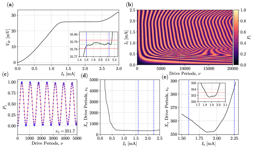
After characterization with the TSCE setup, we establish operating parameters, specifically the rf drive power and dc current bias , for the JPG in which the number of output JPG pulses is equal to the number of input drive periods – called the locking range. Under sinusoidal rf drive at frequency , a constant voltage Shapiro step manifests at
| (3) |
When the measured voltage is constant and equal to Eq. 3 over a range of , then for any on the Shapiro step the device is locked. Thus, we first maximize the locking range by determining the drive power giving the largest Shapiro steps. Fig. 3(a) shows the JPG - curve with maximized locking range.
For all measurements in this work we drive at subharmonic () and use the second harmonic power of the JPG pulse train to control the qubit. As we are restricted to subharmonic drive, maximizes the locking range by making as close as possible to [36] and provides the highest fidelity (fastest) gates. Next, we measure JPG-induced Rabi oscillations to characterize the JPG-qubit interaction. At the optimal drive power we measure the number of drive periods required for a rotation, , versus . Results of this procedure are shown in Fig. 3(b)–(e). Fitting these Rabi oscillations at constant yields and we look for regions where is insensitive to the number of Rabi periods (i.e. drive time). This demonstrates locking of the JPG, where , and a stable JPG-qubit interaction as the drive pattern is lengthened.
One may expect the entire locking range in Fig. 3(a) to give a constant , however, this is not observed in Fig 3(e). This is because the pulse width for Josephson devices operated at varies as traverses the Shapiro step. Widening of the pulses results in a reduction in and is discussed further in the following section, and in Supplementary Material XII. Our simulations for pulse width variation across the Shapiro step agree with previous work [37, 38] and a variation of is expected. This restricts the region of constant in the Rabi measurements relative to the dc locking range measurement. Despite these effects, Fig. 3(e) nevertheless demonstrates a range of 150 A where is constant to within one pulse.
III.2 Finite-Width Pulses
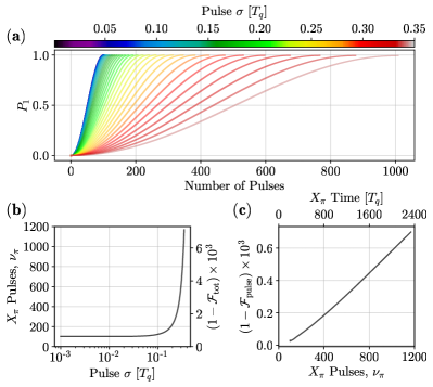
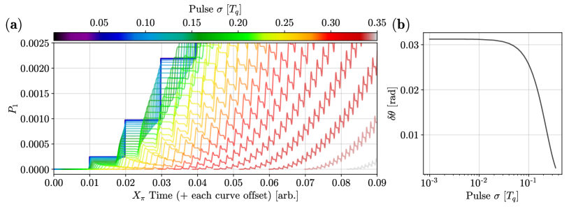
Production of perfectly sharp pulses is not possible, so also depends on JPG pulse width. Indeed, we have demonstrated this by broadening the JPG pulses (we heat the JPG to reduce ) and observe to increase by approximately the same factor decreases. To explore the pulse width dependence of we perform simulations [39] of a qubit driven at by Gaussian pulses whose width (standard deviation in units of the qubit period, ) we control. Fig. 4 shows our simulation results and illustrates a strongly nonlinear dependence on the qubit response for . For short pulses in the Dirac delta function limit , the qubit response is independent of ( changes by less than one pulse). Supplementary Material XIV discusses the relationship between JJ and of a Gaussian fitted to the pulses. For our JPG with ps the (on-chip) Gaussian-parameterized pulse width is ps.
To measure the pulse width, the JPG output is split (see Fig. S1) and recorded with an oscilloscope at room temperature. We find ps which, for our 5.37 GHz qubit, gives . This is an upper bound for the widths of pulses delivered to the qubit due to added dispersion in the additional 2 m of JPG-oscilloscope cabling compared to the JPG-qubit cable length. From the simulations (after adjusting coupling so ) and pulse width measurements we obtain a lower bound of our expected JPG infidelity of . While the total infidelity is coherence-limit-dominated, subtraction of this contribution gives the infidelity due only to the nature of control via digital pulses, . Fig. 4(c) demonstrates that, for our current gate times, this digital-pulse-only infidelity is of the total infidelity. Furthermore, this is competitive with state-of-the-art TSCE techniques, reaching infidelity, and shows there is no fundamental limitation imposed by digital control with sharp pulses 111These simulations were repeated using simulated SFQ pulses with the JPG ps (Supplementary Material XIV) and show no significant change in fidelity.. See Supplementary Material XII for more discussion.
When driven at a frequency below , our prototype JPG’s locking range decreases by a factor but a lower also compromises ideal digital qubit control dynamics. More ideal control may be realized at the expense of locking range (or vice versa) by tuning – with the caveat that pulses are too wide for efficient digital control. We keep to balance locking range and optimal qubit dynamics. Future devices (see Sec. VI) will not possess this limitation.
IV Qubit Performance Comparison
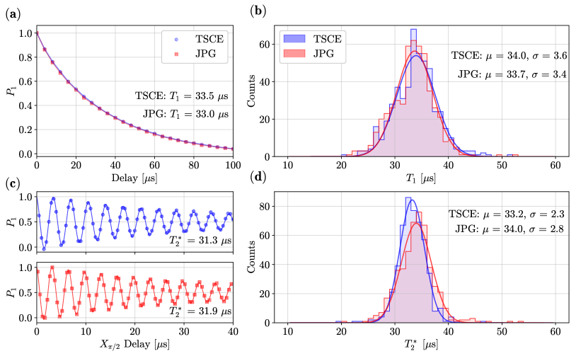
Here we describe the side-by-side comparison of the TSCE and JPG setups through measurements of , , and . For the comparison, a JPG rotation is constructed of drive periods (131 ns drive time) obtained with the calibration shown in Fig. 3. For the comparison a JPG rotation is created with a period drive waveform. We gather statistics on 500 measurements of and with each setup. Data are compiled in Fig. 5 and show energy decay curves and Ramsey fringes averaged over all measurements, as well as histograms of the extracted and . The small discrepancy in the distribution means are well within the expected variation in and for superconducting qubits [41, 42, 27, 43, 4, 44] and within the observed daily fluctuations for this device of s and s for the and mean values, respectively. Indeed, excellent agreement is found in and as measured with each setup – showing that JPG operation does not enhance relaxation or dephasing from quasiparticle poisoning or larger cavity photon number fluctuations.
An important validation of JPG-qubit compatibility is to demonstrate adequate thermalization when controlled with the JPG. State inversions from elevated qubit thermal occupancy can be % in transmon qubits with 3D aluminum readout cavities [45, 46, 47]. We define the qubit thermal occupancy as the probability of incorrect state identification based on the desired preparation.
Measurement of is performed in a two-part experiment [48]. First, no qubit rotation is applied and the state is simply measured. Second, we apply an rotation to invert the qubit population, and then measure. Measurements are single-shot and we do not perform heralding. The total state preparation and measurement (SPAM) fidelity is
| (4) |
where is the probability of measuring state when the qubit was intended to be prepared in . Eq. (4) describes the combined preparation fidelity and ability for the single-shot measurement to correctly distinguish between or . Ideally, each contains contributions only from thermal occupancy. In reality, both include decays from correctly prepared and spuriously excited initial states, and the and distribution overlap. The SPAM fidelity thus gives an upper bound on and we minimize the effects of overlap infidelity and decays during measurement to improve our estimate of .
We limit these decays to , which become the dominant uncertainty in the measurement, by shortening the readout pulse to 400 ns and combat the corresponding reduction of the single-shot SNR using an optimal mode-matching integration weight function [48]. Overlap infidelity is minimized by increasing the cavity drive strength to separate the primary and distribution lobes. For the 400 ns readout pulse this occurs at , which still avoids measurement-induced transitions [35].
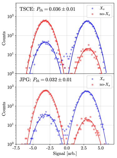
Fig. 6 shows data from measurements with each setup and bimodal Gaussian fits to the data. As the no- case (desired preparation in ) additionally removes decays during preparation, we choose this population to bound with the most accuracy. Integration of all spurious outcomes for this case yields excellent agreement in of and for the TSCE and JPG setups, respectively. These results demonstrate that qubit thermalization is not affected when the JPG is used – our final compatibility metric of digital control using JJ-based pulses from 3 K.
V JPG Randomized Benchmarking
We now characterize JPG gate fidelities through a randomized benchmarking (RB) routine [49, 50, 51, 52, 53] where we apply a sequence of random gates followed by a single sequence-inverting gate. The sequence fidelity is an exponential decay
| (5) |
where the constants and encapsulate SPAM errors and errors on the final gate. For single qubit gates, the depolarizing parameter is related to the per-gate error by
| (6) |
Results of the same routine using the TSCE setup are provided as a reference gate error.
We choose the set of primitive and Pauli gates: {, , , , }, where the idle and gates lengths are equal [54, 55]. Given that gates are twice as long as gates, and the fact we use a Clifford group subset, rescaling by a factor of 1.125 permits comparison to full-Clifford-group RB [52, 21]. JPG gates are constructed as described above, while TSCE gates use a ns Gaussian pulse truncated at to closely match the JPG gate time.
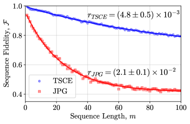
In Fig. 7 we show the results of the RB routine with both setups giving and , where the uncertainties are from the Eq. 5 fit standard error. The JPG is approximately a factor of 10 higher than the simulated single gate error of 222Note that a small measurement error is present in all the JPG RB data, which were taken first and on a separate cooldown than the TSCE RB. This error was remedied before the TSCE measurement was performed and is responsible for the offset in the JPG curve (Fig. 7). We emphasize this has no influence on the extracted for either setup.. Performing a detailed accounting of known possible errors (Supplementary Material XII) from digitization, finite pulse widths, higher state leakage, and pulse timing jitter gives an estimated infidelity of . This is a factor of three below the RB result. We attribute the remaining error to possible systematic or coherent errors which are presently under investigation. Regardless, these measurements serve as an excellent proof-of-concept demonstration of qubit control using 3 K JJ-based digital pulses.
VI Scalability and Discussion of Future Devices
The scalability of digital qubit control using JJ devices at 3 K is promising even with the current device and configuration – which were not optimized for size or power dissipation. The JPG circuit is mm2 and the power dissipated at duty cycle is approximately
| (7) |
For the maximum in our experiment of 0.02, this yields W. Commercial cryocoolers delivering W of cooling power at 3 K [57] permit use of over 500k similar devices; occupying m3. The JPG pulse output power is dBm (at ), giving off-chip dissipation of the qubit drive signal of {2 nW, 0.3 nW, 0.02 nW, 0.008 nW} at the {3 K, 1 K, 0.05 K, 0.01 K} stages (see Supplementary Material VIII for details of the JPG control line attenuation stack). Of larger consideration is dissipation of the large drive signal, which is dBm at the JPG input at 3 K, however the new devices discussed below offer techniques to circumvent this limitation.
Plans for NISQ systems require m3 of cryostat volume and numerous cryocoolers. We conclude that neither power dissipation, nor device size (volume of silicon) present significant obstacles in scaling the number of 3 K JJ devices to control NISQ-era quantum arrays. Furthermore, our experimental and JPG architectures can both be adjusted in a straightforward manner to reduce device size and on-chip power dissipation each by more than a factor of 10. Thus, the primary obstacle in scaling a 3 K JJ-based qubit control architecture, at least in the near-term, is one shared by many competing qubit control technologies: wiring and signal routing logistics. Multi-chip modules [58, 59, 60], high-density/bandwidth interconnects [28, 30], and out-of-plane coupling [61] make overcoming these challenges feasible.
The present experiment architecture, where JPG pulses are heavily attenuated by the cavity resonance before reaching the qubit, necessitates use of a large to yield appropriate signal levels. This increases device size, power dissipation, and can reduce qubit coherence by allowing the higher pulse train harmonics to populate the cavity (not observed here). These limitations can be eliminated using 2D readout cavity qubit devices and an independent control line. With such a device we expect to reduce the array factor to without sacrificing thermalization or gate time.
Next-generation devices will implement an SFQ logic shift register and voltage multiplier pulse amplification with no increase in JJ count [16, 62]. Use of a high speed clock far above the qubit spectrum eliminates the qubit-drive interaction and permits pulse delivery at or at variable timing. The latter has been theoretically shown to reach 99.99% fidelity with under 10 ns gates [19]. Voltage multiplier amplification minimizes on-chip dispersion and permits narrower output pulses; enabling more ideal digital qubit dynamics. Finally, these devices permit signal routing which eliminates dissipation of the drive signal in cryogenic attenuators, which is a major consideration for the present JPG device and would strongly limit scaling of these prototype devices.
VII Conclusion
In this article we have demonstrated, for the first time, successful digital control of a transmon qubit at 0.01 K using a superconducting Josephson pulse generator located at 3 K. Through dual characterization of the system, using both traditional semiconductor control electronics [5] and the 3 K JPG, we see no reduction in intrinsic qubit performance. Specifically we measured no negative impact to , , or – indicative that quasiparticle propagation is effectively broken by locating the JJ elements and quantum circuits on separate temperature stages. Additionally, we measure an average JPG gate error of which, considering the improvements of the future JJ devices discussed in the previous section, are expected to reach the simulated coherence-dominated infidelity of .
These results enable scaled quantum information systems which leverage the merits of Josephson-based sources for qubit control: signal stability, reproducibility, SFQ pulse self-calibration, small device size, and low power dissipation. Straightforward alterations in the qubit and JPG architectures enable factors of reduction in dissipation and size, and future devices are expected to bring JJ-based digital gates into competition with contemporary TSCE gates. Such improvements further increase the potential value of 3 K JJ-based qubit control, as current device sizes and dissipation are commensurate with operation of over 500k devices. Integration with cryoCMOS devices [9, 8, 10] is also possible; potentially yielding a hybrid cryogenic controller exploiting the advantages of both technologies.
Acknowledgements.
We acknowledge the NIST Advanced Microwave Photonics Group for the qubit, JPA, and readout microwave components. We thank N. Flowers-Jacobs for readout microwave components. We thank F. Lecocq, R. McDermott, and B Plourde for fruitful discussions, and A. Babenko and A. Fox for design and fabrication of initial devices. L. Howe was funded through the NRC Postdoctoral Research Associateship Program.References
- Fowler et al. [2012] A. G. Fowler, M. Mariantoni, J. M. Martinis, and A. N. Cleland, Surface codes: Towards practical large-scale quantum computation, Phys. Rev. A 86, 032324 (2012).
- Kelly et al. [2015] J. Kelly, R. Barends, A. G. Fowler, A. Megrant, E. Jeffrey, T. C. White, D. Sank, J. Y. Mutus, B. Campbell, Y. Chen, et al., State preservation by repetitive error detection in a superconducting quantum circuit, Nature 519, 66 (2015).
- Andersen et al. [2020] C. K. Andersen, A. Remm, S. Lazar, S. Krinner, N. Lacroix, G. J. Norris, M. Gabureac, C. Eichler, and A. Wallraff, Repeated quantum error detection in a surface code, Nature Physics 16, 875 (2020).
- Google Quantum AI [2021] Google Quantum AI, Exponential suppression of bit or phase errors with cyclic error correction, Nature 595, 383 (2021).
- Krantz et al. [2019] P. Krantz, M. Kjaergaard, F. Yan, T. P. Orlando, S. Gustavsson, and W. D. Oliver, A quantum engineer’s guide to superconducting qubits, Applied Physics Reviews 6, 021318 (2019).
- Krinner et al. [2019] S. Krinner, S. Storz, P. Kurpiers, P. Magnard, J. Heinsoo, R. Keller, J. Luetolf, C. Eichler, and A. Wallraff, Engineering cryogenic setups for 100-qubit scale superconducting circuit systems, EPJ Quantum Technology 6, 2 (2019).
- van Dijk et al. [2019] J. van Dijk, E. Kawakami, R. Schouten, M. Veldhorst, L. Vandersypen, M. Babaie, E. Charbon, and F. Sebastiano, Impact of Classical Control Electronics on Qubit Fidelity, Phys. Rev. Applied 12, 044054 (2019).
- Van Dijk et al. [2020] J. P. G. Van Dijk, B. Patra, S. Subramanian, X. Xue, N. Samkharadze, A. Corna, C. Jeon, F. Sheikh, E. Juarez-Hernandez, B. P. Esparza, H. Rampurawala, B. R. Carlton, S. Ravikumar, C. Nieva, S. Kim, et al., A Scalable Cryo-CMOS Controller for the Wideband Frequency-Multiplexed Control of Spin Qubits and Transmons, IEEE Journal of Solid-State Circuits 55, 2930 (2020).
- Bardin et al. [2019] J. C. Bardin, E. Jeffrey, E. Lucero, T. Huang, S. Das, D. T. Sank, O. Naaman, A. E. Megrant, R. Barends, T. White, M. Giustina, K. J. Satzinger, K. Arya, P. Roushan, B. Chiaro, et al., Design and Characterization of a 28-nm Bulk-CMOS Cryogenic Quantum Controller Dissipating Less Than 2 mW at 3 K, IEEE Journal of Solid-State Circuits 54, 3043 (2019).
- Pauka et al. [2021] S. Pauka, K. Das, R. Kalra, A. Moini, Y. Yang, M. Trainer, A. Bousquet, C. Cantaloube, N. Dick, G. Gardner, et al., A cryogenic CMOS chip for generating control signals for multiple qubits, Nature Electronics 4, 64 (2021).
- Sirois et al. [2020] A. J. Sirois, M. Castellanos-Beltran, A. E. Fox, S. P. Benz, and P. F. Hopkins, Josephson Microwave Sources Applied to Quantum Information Systems, IEEE Transactions on Quantum Engineering 1, 1 (2020).
- Ball et al. [2016] H. Ball, W. D. Oliver, and M. J. Biercuk, The role of master clock stability in quantum information processing, npj Quantum Information 2, 1 (2016).
- Rüfenacht et al. [2015] A. Rüfenacht, L. A. Howe, A. E. Fox, R. E. Schwall, P. D. Dresselhaus, C. J. Burroughs, S. P. Benz, and S. P. Benz, Cryocooled 10 V Programmable Josephson Voltage Standard, IEEE Transactions on Instrumentation and Measurement 64, 1477 (2015).
- Burroughs et al. [2011] C. J. Burroughs, P. D. Dresselhaus, A. Rufenacht, D. Olaya, M. M. Elsbury, Y.-H. Tang, and S. P. Benz, NIST 10 V Programmable Josephson Voltage Standard System, IEEE Transactions on Instrumentation and Measurement 60, 2482 (2011).
- Brevik et al. [2018] J. A. Brevik, C. A. Donnelly, N. E. Flowers-Jacobs, A. E. Fox, P. F. Hopkins, P. D. Dresselhaus, and S. P. Benz, Radio-Frequency Waveform Synthesis with the Josephson Arbitrary Waveform Synthesizer, 2018 Conference on Precision Electromagnetic Measurements , 1 (2018).
- Hopkins et al. [2019] P. F. Hopkins, J. A. Brevik, M. Castellanos-Beltran, C. A. Donnelly, N. E. Flowers-Jacobs, A. E. Fox, D. Olaya, P. D. Dresselhaus, and S. P. Benz, RF Waveform Synthesizers With Quantum-Based Voltage Accuracy for Communications Metrology, IEEE Transactions on Applied Superconductivity 29, 1 (2019).
- Rüfenacht et al. [2018] A. Rüfenacht, N. E. Flowers-Jacobs, and S. P. Benz, Impact of the latest generation of Josephson voltage standards in ac and dc electric metrology, Metrologia 55, S152 (2018).
- McDermott and Vavilov [2014] R. McDermott and M. G. Vavilov, Accurate Qubit Control with Single Flux Quantum Pulses, Phys. Rev. Applied 2, 014007 (2014).
- Liebermann and Wilhelm [2016] P. J. Liebermann and F. K. Wilhelm, Optimal Qubit Control Using Single-Flux Quantum Pulses, Phys. Rev. Applied 6, 024022 (2016).
- McDermott et al. [2018] R. McDermott, M. G. Vavilov, B. L. T. Plourde, F. K. Wilhelm, P. J. Liebermann, O. A. Mukhanov, and T. A. Ohki, Quantum–classical interface based on single flux quantum digital logic, Quantum Science and Technology 3, 024004 (2018).
- Leonard et al. [2019] E. Leonard, M. A. Beck, J. Nelson, B. Christensen, T. Thorbeck, C. Howington, A. Opremcak, I. Pechenezhskiy, K. Dodge, N. Dupuis, M. Hutchings, J. Ku, F. Schlenker, J. Suttle, C. Wilen, et al., Digital Coherent Control of a Superconducting Qubit, Phys. Rev. Applied 11, 014009 (2019).
- Patel et al. [2017] U. Patel, I. V. Pechenezhskiy, B. L. T. Plourde, M. G. Vavilov, and R. McDermott, Phonon-mediated quasiparticle poisoning of superconducting microwave resonators, Phys. Rev. B 96, 220501 (2017).
- Martinis et al. [2009] J. M. Martinis, M. Ansmann, and J. Aumentado, Energy Decay in Superconducting Josephson-Junction Qubits from Nonequilibrium Quasiparticle Excitations, Phys. Rev. Lett. 103, 097002 (2009).
- Ballard et al. [2021] A. Ballard, V. Iaia, T. McBroom, Y. Liu, K. Dodge, J. Ku, C.-H. Liu, A. Opremcak, C. Wilen, E. Leonard, et al., Single Flux Quantum-Based Superconducting Qubit Control and Quasiparticle Mitigation: Part I, Bulletin of the American Physical Society (2021).
- Liu et al. [2021] C. Liu, A. Opremcak, C. Wilen, E. Leonard, M. Beck, S. Abdullah, A. Ballard, V. Iaia, T. McBroom, Y. Liu, et al., Single Flux Quantum-Based Superconducting Qubit Control and Quasiparticle Mitigation: Part 2, Bulletin of the American Physical Society (2021).
- Hosseinkhani et al. [2017] A. Hosseinkhani, R.-P. Riwar, R. J. Schoelkopf, L. I. Glazman, and G. Catelani, Optimal Configurations for Normal-Metal Traps in Transmon Qubits, Phys. Rev. Applied 8, 064028 (2017).
- Martinis [2021] J. M. Martinis, Saving superconducting quantum processors from decay and correlated errors generated by gamma and cosmic rays, npj Quantum Information 7, 1 (2021).
- Smith et al. [2020] J. P. Smith, B. A. Mazin, A. B. Walter, M. Daal, J. Bailey III, C. Bockstiegel, N. Zobrist, N. Swimmer, S. Steiger, and N. Fruitwala, Flexible coaxial ribbon cable for high-density superconducting microwave device arrays, IEEE Transactions on Applied Superconductivity 31, 1 (2020).
- Walter et al. [2018] A. B. Walter, C. Bockstiegel, B. A. Mazin, and M. Daal, Laminated NbTi-on-Kapton Microstrip Cables for Flexible Sub-Kelvin RF Electronics, IEEE Transactions on Applied Superconductivity 28, 1 (2018).
- Tuckerman et al. [2016] D. B. Tuckerman, M. C. Hamilton, D. J. Reilly, R. Bai, G. A. Hernandez, J. M. Hornibrook, J. A. Sellers, and C. D. Ellis, Flexible superconducting Nb transmission lines on thin film polyimide for quantum computing applications, Superconductor Science and Technology 29, 084007 (2016).
- Tinkham [2004] M. Tinkham, Introduction to superconductivity (Courier Corporation, 2004).
- Lecocq et al. [2021] F. Lecocq, F. Quinlan, K. Cicak, J. Aumentado, S. Diddams, and J. Teufel, Control and readout of a superconducting qubit using a photonic link, Nature 591, 575 (2021).
- Bianchetti et al. [2009] R. Bianchetti, S. Filipp, M. Baur, J. M. Fink, M. Göppl, P. J. Leek, L. Steffen, A. Blais, and A. Wallraff, Dynamics of dispersive single-qubit readout in circuit quantum electrodynamics, Phys. Rev. A 80, 043840 (2009).
- Castellanos-Beltran and Lehnert [2007] M. Castellanos-Beltran and K. Lehnert, Widely tunable parametric amplifier based on a superconducting quantum interference device array resonator, Applied Physics Letters 91, 083509 (2007).
- Sank et al. [2016] D. Sank, Z. Chen, M. Khezri, J. Kelly, R. Barends, B. Campbell, Y. Chen, B. Chiaro, A. Dunsworth, A. Fowler, E. Jeffrey, E. Lucero, A. Megrant, J. Mutus, M. Neeley, et al., Measurement-Induced State Transitions in a Superconducting Qubit: Beyond the Rotating Wave Approximation, Phys. Rev. Lett. 117, 190503 (2016).
- Benz and Hamilton [1996] S. P. Benz and C. A. Hamilton, A pulse-driven programmable Josephson voltage standard, Applied physics letters 68, 3171 (1996).
- Donnelly et al. [2020] C. A. Donnelly, N. E. Flowers-Jacobs, J. A. Brevik, A. E. Fox, P. D. Dresselhaus, P. F. Hopkins, and S. P. Benz, 1 GHz Waveform Synthesis With Josephson Junction Arrays, IEEE Transactions on Applied Superconductivity 30, 1 (2020).
- Babenko et al. [2020] A. A. Babenko, A. S. Boaventura, N. E. Flowers-Jacobs, J. A. Brevik, A. E. Fox, D. F. Williams, Z. Popović, P. D. Dresselhaus, and S. P. Benz, Characterization of a Josephson Junction Comb Generator, in 2020 IEEE/MTT-S International Microwave Symposium (IMS) (2020) pp. 936–939.
- Johansson et al. [2012] J. R. Johansson, P. D. Nation, and F. Nori, QuTiP: An open-source Python framework for the dynamics of open quantum systems, Computer Physics Communications 183, 1760 (2012).
- Note [1] These simulations were repeated using simulated SFQ pulses with the JPG ps (Supplementary Material XIV) and show no significant change in fidelity.
- Burnett et al. [2019] J. J. Burnett, A. Bengtsson, M. Scigliuzzo, D. Niepce, M. Kudra, P. Delsing, and J. Bylander, Decoherence benchmarking of superconducting qubits, npj Quantum Information 5, 1 (2019).
- Vepsäläinen et al. [2020] A. P. Vepsäläinen, A. H. Karamlou, J. L. Orrell, A. S. Dogra, B. Loer, F. Vasconcelos, D. K. Kim, A. J. Melville, B. M. Niedzielski, J. L. Yoder, et al., Impact of ionizing radiation on superconducting qubit coherence, Nature 584, 551 (2020).
- McRae et al. [2020] C. R. H. McRae, H. Wang, J. Gao, M. R. Vissers, T. Brecht, A. Dunsworth, D. P. Pappas, and J. Mutus, Materials loss measurements using superconducting microwave resonators, Review of Scientific Instruments 91, 091101 (2020).
- McEwen et al. [2021] M. McEwen, L. Faoro, K. Arya, A. Dunsworth, T. Huang, S. Kim, B. Burkett, A. Fowler, F. Arute, J. C. Bardin, et al., Resolving catastrophic error bursts from cosmic rays in large arrays of superconducting qubits, arXiv preprint arXiv:2104.05219 (2021).
- Wenner et al. [2013] J. Wenner, Y. Yin, E. Lucero, R. Barends, Y. Chen, B. Chiaro, J. Kelly, M. Lenander, M. Mariantoni, A. Megrant, C. Neill, P. J. J. O’Malley, D. Sank, A. Vainsencher, H. Wang, et al., Excitation of Superconducting Qubits from Hot Nonequilibrium Quasiparticles, Phys. Rev. Lett. 110, 150502 (2013).
- Jin et al. [2015] X. Y. Jin, A. Kamal, A. P. Sears, T. Gudmundsen, D. Hover, J. Miloshi, R. Slattery, F. Yan, J. Yoder, T. P. Orlando, S. Gustavsson, and W. D. Oliver, Thermal and Residual Excited-State Population in a 3D Transmon Qubit, Phys. Rev. Lett. 114, 240501 (2015).
- Jeffrey et al. [2014] E. Jeffrey, D. Sank, J. Y. Mutus, T. C. White, J. Kelly, R. Barends, Y. Chen, Z. Chen, B. Chiaro, A. Dunsworth, A. Megrant, P. J. J. O’Malley, C. Neill, P. Roushan, A. Vainsencher, et al., Fast Accurate State Measurement with Superconducting Qubits, Phys. Rev. Lett. 112, 190504 (2014).
- Walter et al. [2017] T. Walter, P. Kurpiers, S. Gasparinetti, P. Magnard, A. Potočnik, Y. Salathé, M. Pechal, M. Mondal, M. Oppliger, C. Eichler, and A. Wallraff, Rapid High-Fidelity Single-Shot Dispersive Readout of Superconducting Qubits, Phys. Rev. Applied 7, 054020 (2017).
- Knill et al. [2008] E. Knill, D. Leibfried, R. Reichle, J. Britton, R. B. Blakestad, J. D. Jost, C. Langer, R. Ozeri, S. Seidelin, and D. J. Wineland, Randomized benchmarking of quantum gates, Phys. Rev. A 77, 012307 (2008).
- Magesan et al. [2012] E. Magesan, J. M. Gambetta, B. R. Johnson, C. A. Ryan, J. M. Chow, S. T. Merkel, M. P. da Silva, G. A. Keefe, M. B. Rothwell, T. A. Ohki, M. B. Ketchen, and M. Steffen, Efficient Measurement of Quantum Gate Error by Interleaved Randomized Benchmarking, Phys. Rev. Lett. 109, 080505 (2012).
- Magesan et al. [2011] E. Magesan, J. M. Gambetta, and J. Emerson, Scalable and Robust Randomized Benchmarking of Quantum Processes, Phys. Rev. Lett. 106, 180504 (2011).
- Chen [2018] Z. Chen, Metrology of quantum control and measurement in superconducting qubits, Ph.D. thesis, UC Santa Barbara (2018).
- Rol et al. [2017] M. A. Rol, C. C. Bultink, T. E. O’Brien, S. R. de Jong, L. S. Theis, X. Fu, F. Luthi, R. F. L. Vermeulen, J. C. de Sterke, A. Bruno, D. Deurloo, R. N. Schouten, F. K. Wilhelm, and L. DiCarlo, Restless Tuneup of High-Fidelity Qubit Gates, Phys. Rev. Applied 7, 041001 (2017).
- Petit et al. [2020] L. Petit, H. Eenink, M. Russ, W. Lawrie, N. Hendrickx, S. Philips, J. Clarke, L. Vandersypen, and M. Veldhorst, Universal quantum logic in hot silicon qubits, Nature 580, 355 (2020).
- McKay et al. [2019] D. C. McKay, S. Sheldon, J. A. Smolin, J. M. Chow, and J. M. Gambetta, Three-Qubit Randomized Benchmarking, Phys. Rev. Lett. 122, 200502 (2019).
- Note [2] Note that a small measurement error is present in all the JPG RB data, which were taken first and on a separate cooldown than the TSCE RB. This error was remedied before the TSCE measurement was performed and is responsible for the offset in the JPG curve (Fig. 7). We emphasize this has no influence on the extracted for either setup.
- Tsan et al. [2021] T. Tsan, N. Galitzki, A. M. Ali, K. Arnold, G. Coppi, T. Ervin, L. Foote, B. Keating, J. Lashner, J. Orlowski-Scherer, M. J. Randall, J. Seibert, J. Spisak, G. P. Teply, Z. Xu, et al., The effects of inclination on a two stage pulse tube cryocooler for use with a ground based observatory, Cryogenics 117, 103323 (2021).
- Holman et al. [2021] N. Holman, D. Rosenberg, D. Yost, J. Yoder, R. Das, W. D. Oliver, R. McDermott, and M. Eriksson, 3D integration and measurement of a semiconductor double quantum dot with a high-impedance TiN resonator, npj Quantum Information 7, 1 (2021).
- Gold et al. [2021] A. Gold, J. Paquette, A. Stockklauser, M. J. Reagor, M. S. Alam, A. Bestwick, N. Didier, A. Nersisyan, F. Oruc, A. Razavi, et al., Entanglement across separate silicon dies in a modular superconducting qubit device, npj Quantum Information 7, 1 (2021).
- Hidaka [2019] M. Hidaka, Japanese Activities for Superconducting Circuits Using Flip-chip Configurations, IEEE CSC and ESAS Superconductivity News Forum (2019).
- Rahamim et al. [2017] J. Rahamim, T. Behrle, M. Peterer, A. Patterson, P. Spring, T. Tsunoda, R. Manenti, G. Tancredi, and P. Leek, Double-sided coaxial circuit QED with out-of-plane wiring, Applied Physics Letters 110, 222602 (2017).
- Castellanos-Beltran et al. [2021] M. A. Castellanos-Beltran, D. I. Olaya, A. J. Sirois, C. A. Donnelly, P. D. Dresselhaus, S. Benz, and P. F. Hopkins, Single-Flux-Quantum Multiplier Circuits for Synthesizing Gigahertz Waveforms With Quantum-Based Accuracy, IEEE Transactions on Applied Superconductivity 31, 1 (2021).
- Rylyakov and Likharev [1999] A. V. Rylyakov and K. K. Likharev, Pulse jitter and timing errors in RSFQ circuits, IEEE transactions on applied superconductivity 9, 3539 (1999).
- Fox et al. [2015] A. E. Fox, P. D. Dresselhaus, A. Rüfenacht, A. Sanders, and S. P. Benz, Junction Yield Analysis for 10 V Programmable Josephson Voltage Standard Devices, IEEE Transactions on Applied Superconductivity 25, 1 (2015).
Supplementary Material: Digital control of a superconducting qubit using a Josephson pulse generator at 3 K
VIII Full Experimental Schematic
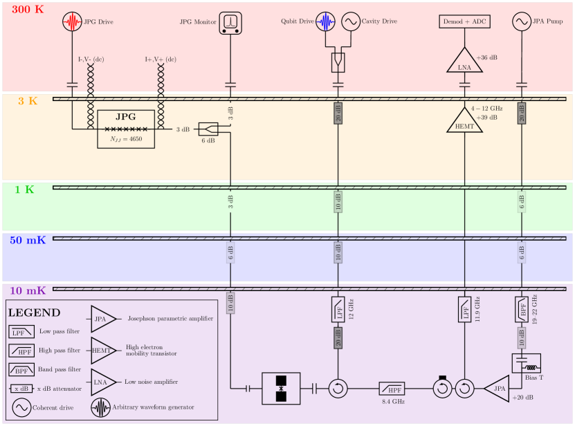
We present the full experimental diagram in Fig. S1. The JPG has two sets of twisted pair leads connected to on-chip inductive taps to permit low-frequency - characterization of the JPG. A splitter is also used on the JPG rf output line for analysis of high frequency characteristics using ambient instrumentation. A 2.85 GHz low pass filter with over 60 dB insertion loss at 5 GHz is used at 300 K to fully prevent any higher harmonic content of the JPG clock signal from driving the qubit.
IX Rabi and Ramsey Frequency Sweeps
In Fig. S2 we present generalized Rabi and Ramsey scans where we sweep the JPG drive frequency . This is simply a demonstration that we may make connection with various routines and protocols with the JPG that are common with TSCE control setups.
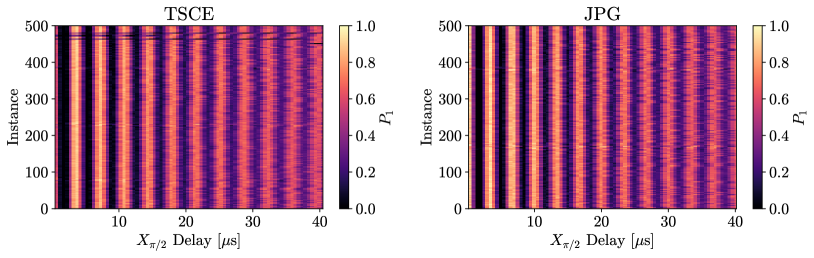
X Ramsey Fringe Compilation
XI Orthogonal Axis Control and Construction of JPG Drive Waveforms
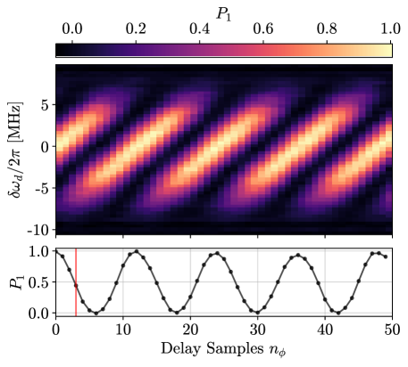
Here we provide details of JPG drive waveforms and the procedure to establish and verify orthogonal axis control of the qubit. For orthogonal control, first a timing reference is established to define the control axis (). At subharmonic drive the control axis is realized by phasing the drive signal to allow the qubit to precess by before the control pulse train arrives [21]. Intuitively, there are qubit periods per drive period and during each qubit period the qubit phase advances relative to the drive by a factor . Therefore, to accumulate the required in a single drive period, the drive signal must be phased by relative to the drive timing reference.
Drive waveforms are constructed from sine waves with an integer number of samples per sine period with the integer chosen to be compatible with the DAC sample rate of the AWG and also results in synthesis at the proper drive frequency. For all qubit control experiments we generate JPG pulses at the qubit subharmonic and use sine periods of length 24 samples, leading to an AWG clock frequency of 64.32 GSa/s to synthesize 2.68 GHz clocking sine pulses. For the expected delay required for rotations is .
Phasing between the timing reference (in-phase drive) and the control axis is verified by performing a Ramsey-like experiment. The JPG clock frequency is swept, as well as the delay between two “” pulses. I.e. we begin with zero delay, yielding an pulse, and increase the delay by inserting a number of zero delay samples until the rotation sequence is observed. Thus the signature of the axis calibration experiment will be a measurement of the qubit in the state () and decreasing to an equal () superposition when the proper phase () is reached. Oscillations then proceed with a period of delay samples as the required delay in the qubit frame is one-fourth of a period. An example of this calibration routine in shown in Fig. S4.
For the JPG RB tests we note that there are often subsets of the full pattern resembling , or gate combinations. Referring to Fig. 1(d), we see that to construct a rotation, the phase of the drive must be delayed relative to the initial timing reference by . Similarly, to achieve an rotation immediately following a rotation, the drive phase must be advanced by the same amount to re-establish the null timing reference phase. To this end, every and JPG waveform is periods in length. There are periods of active drive, with the additional two periods of idle divided appropriately at the beginning and end of the waveform to permit delaying and advancing the drive phase as needed. The same procedure is followed for and rotations. Due to the unidirectional nature of digital qubit control using a JPG, rotations are achieved using and phases relative to the timing reference (we take and as the ideal final states are identical to those from positive gates). Note that, for both positive and negative rotations, the drive signals are equal in length as described above.
XII Digital Qubit Control Fidelity Limits
Multiple factors arise in a digital qubit control architecture which affect fidelity and are not present in systems using TSCE-based microwave pulses. They are: digitization error, error due to the finite temporal width of the digital pulses, higher state leakage of the pulse train spectrum due to finite qubit anharmonicity, and pulse arrival timing jitter.
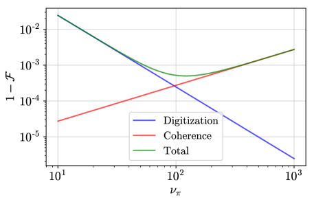
Digitization error arises from eliminating the continuous variable corresponding to the pulse power and manifests as a maximal over- or under-rotation by (at most) pulse. The digitization error is
| (S1) |
which decreases as increases. With finite qubit coherence time a sweet spot arises which minimizes the infidelity, as is shown in Fig. S5. Note that as the qubit lifetime increases the value of which minimizes the combined digitization and coherence-limited infidelity also increases. For the digitization infidelity of is much smaller than the infidelity due to qubit coherence.
The second affect on the gate fidelity is due to the finite temporal width of the control pulses. As discussed in the main text, Sec. III.2, we simulate these effects [39] using a train of Gaussian pulses delivered at to evolve the qubit state and study the fidelity of rotations as a function of the pulse standard deviation . The Hamiltonian for the system is
| (S2) |
where and describe the coupling strength and the pulse train time-dependent amplitude, respectively. Note that due to the pulse drive’s time-dependent nature we cannot make a rotating wave approximation. Since our simulations use a true two-level system, there is no leakage outside of {, } so can be used to calculate the fidelity . To determine we evaluate only at the center of the idle qubit period following a pulse and take the resultant maximum value as . This also defines the value of , i.e. the number of pulses which maximize the following idle qubit period as a function of . As is increased, the pulse train power at the second harmonic, and thus the tip angle per pulse, , diminishes so more pulses are required to realize a rotation with wider pulses (this is in conjunction with distributed pulse energy delivery as the qubit precesses, discussed below). In turn, increases so we must recalculate at each pulse width. For these simulations we include loss with realistic values of s (s) for our qubit. Fig. 4 in the main body shows the Rabi oscillation curves, , and the corresponding fidelity.
If the Gaussian pulse duration () approaches , the pulses no longer deliver the majority of their power when the qubit is aligned with the desired control axes. Rather, the pulses turn on and off slowly relative to the qubit period and their action is distributed over a non-negligible portion of the qubit precession. For a wide pulse near its peak, the pulse delivers the majority of its energy and rotates the qubit state along the target control axis. However, the long tails before and after the peak impart lesser rotations while the qubit advances phase at . As the qubit precesses, moves through having a component anti-aligned with the target control axis, to being aligned, and then anti-aligned, etc. In the anti-alignment phase the leading and trailing pulse tails induce small negative (back towards ) rotations on either side of the main positive rotation; corresponding to the pulse maximum and complete alignment of and the target control axis. This behavior manifests as a dip in when the pulse begins to arrive, a larger increase in as the pulse peak arrives, and another small reduction in for the trailing pulse tail.
To demonstrate these effects, Fig. S6 shows a magnified view of the qubit excited state evolution for the first few pulses and as the pulse is swept, as well as the reduction in as increases. We find that for wide pulses () the infidelity, after subtraction of the coherence limit contribution, roughly corresponds to the rotation lost due to pulse energy delivery while the qubit is anti-aligned with the desired control axis. In the main text we refer to this as the digital-pulse-only infidelity, . As stated in Fig 4(c), for , we expect . This is over an order of magnitude smaller than the coherence-limit contribution as we find with finite coherence.
Leakage to the higher transmon level arises from the finite length pulse train used to evolve the qubit state. To estimate the infidelity due to higher state leakage we follow analysis in [18], which uses and true Dirac delta function pulses. Since we rescale by a factor . For our qubit, with an anharmonicity , this results in higher state leakage infidelity of . We note that for our case of moderate-width pulses, the ringing in the pulse train spectrum will be further suppressed relative to the Dirac delta function pulse train in [18].
For our configuration we consider the case of pulse timing jitter when the JPG is driven with a stable external clock [18]. Gaussian-distributed thermal jitter in pulse generation in SFQ circuitry has been measured to have a standard deviation of 3 ps or less at 4.2 K [63]. However, for an array, the effect of thermal jitter at each JJ results only in a slight broadening of the output JPG pulse with little effect on the pulse arrival time. Timing jitter from the JPG drive signal, however, will cause jitter of the JPG output signal. Measurements of jitter in the JPG drive signal at 300 K indicate jitter of 3 ps (standard deviation), corresponding to a jitter-sourced infidelity estimate of .
Combining all contributions above we obtain a total expected gate infidelity of , a factor of three lower than the observed JPG RB error per gate of . We attribute the unaccounted infidelity to possible systematic and coherent errors in the RB routine and are actively investigating these effects.
XIII JPG Fabrication details and Reduced Temperature Sensitivity
Gating pulses from a JJ array with our scheme of driving with an integer number of pure sine periods means the rf dissipation is toggled rapidly between null and 100%. Depending on the temperature sensitivity, this can cause an unstable locking range for a JJ array and make calibrations such as those detailed in Fig. 3 difficult or impossible.
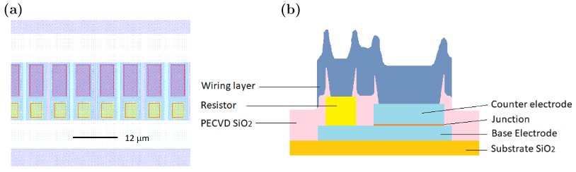
To reduce the temperature sensitivity of the JPG we have departed from the superconductor-normal metal-superconductor (SNS) JJ technology [64] based on triple-stacked self-shunted niobium-doped-silicon barriers (NbSi) embedded in the center conductor of a niobium (Nb) superconducting coplanar waveguide. Instead, we form the JPG array from externally shunted superconductor-insulator-superconductor (SIS) junctions, as can be seen in Fig. S7(a). The JJs were fabricated using amorphous silicon (Si) for the barriers and palladium-gold (PdAu) alloy for shunting resistors. Due to the small value of the shunting resistors (25 m) required to achieve the target characteristic frequency of GHz, the usual method of fabricating planar resistors could not be used. That method relies on resistor films with sheet resistances of 1–2 . The form factor to achieve 25 m entails very wide and long arrays to accommodate interconnecting vias to minimize contact resistance. Instead, (vertical) stud resistors were used with a height similar to the junction counter electrode thickness. See a schematic of the cross-section in Fig. S7(b). This enables significant reduction in the JJ cell size and results in a much more compact array.
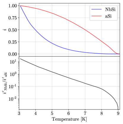
The circuits were fabricated on 3-inch silicon wafers with 150 nm of thermal oxide. A trilayer of Nb/Si/Nb was deposited by sputtering. The thickness of the silicon was chosen to obtain a junction critical current density of 12 kA/cm2. PdAu resistors were electron-beam evaporated with a thickness of 240 nm. Silicon oxide insulator was then deposited by electron cyclotron plasma enhanced chemical vapor deposition (EC-PECVD). Lithography followed by dry etching opened vias to the junction counter electrodes, resistors, and base electrodes. The wiring layer was deposited by niobium sputtering and then patterned by dry etching. Resulting devices display mA and m, giving GHz. These devices exploit the much more stable of Si barrier JJs with respect to temperature. Fig S8 shows a comparison of the temperature stability of for NbSi and Si devices, demonstrating that in our region of interest of 3–3.3 K the Si barrier device is – times less sensitive.
XIV Relation Between JPG and Gaussian-fitted
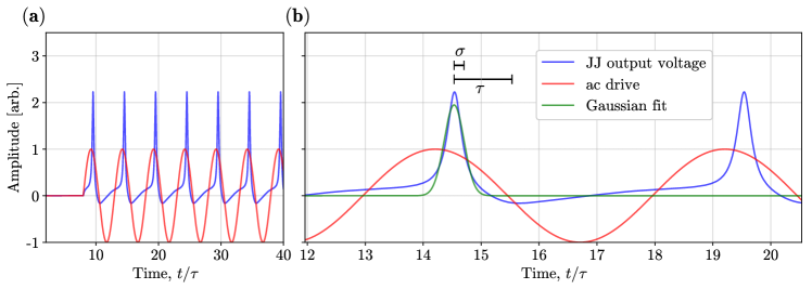
Simulations of JPG dynamics can be performed by numerically integrating the resistively shunted junction (RSJ) model with an ac drive term
| (S3) |
Here is the superconducting phase difference across the JJ, is the dimensionless time variable , is the Stewart-McCumber damping parameter with the intrinsic JJ shunting capacitance, and and are the normalized dc and ac (amplitude) bias currents, respectively. Note that the ac drive frequency has units of time scaled to the Josephson time constant and not to , as these differ by a factor of .
With the second Josephson equation
| (S4) |
and Eq. S3, we can solve for the time-dependent voltage response of the JJ. We choose , and , which approximately reflects the relation between the JPG of 10.2 GHz and the typical drive frequency of GHz, and ramp until pulses are observed. For , the JJ response is overdamped and non-hysteretic so we simulate a heavily overdamped regime of . For our JPG, . Results are displayed in Fig S9 and we perform a Gaussian fit to one SFQ pulse. Time units are re-scaled from the time of Eq S3 to units of the JJ characteristic time . For these parameters we extract . This indicates that, given the JPG of 98 ps, the pulses at 3 K (on-chip, prior to any significant dispersion and broadening) have an expected Gaussian sigma of 17 ps. Fits at room temperature of the JPG pulses captured on the oscilloscope (Sec. III.2 of main body) thus display approximately a factor of two in broadening compared to the expected on-chip value. As mentioned in Sec. III.2, this is the reason we take ps to be a conservative upper bound on the approximate width of pulses delivered to the qubit, even after traversal of the readout cavity resonance.