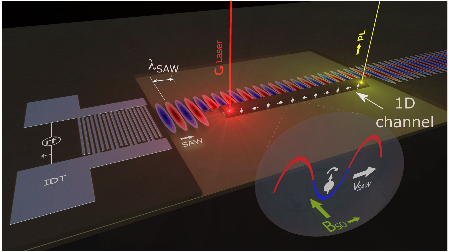
Flying electron spin control gates
Abstract
The control of "flying" (or moving) spin qubits is an important functionality for the manipulation and exchange of quantum information between remote locations on a chip. Typically, gates based on electric or magnetic fields provide the necessary perturbation for their control either globally or at well-defined locations. Here, we demonstrate the dynamic control of moving electron spins via contactless gates that move together with the spin. The concept is realized using electron spins trapped and transported by moving potential dots defined by a surface acoustic wave (SAW). The SAW strain at the electron trapping site, which is set by the SAW amplitude, acts as a contactless, tunable gate that controls the precession frequency of the flying spins via the spin-orbit interaction. We show that the degree of precession control in moving dots exceeds previously reported results for unconstrained transport by an order of magnitude and is well accounted for by a theoretical model for the strain contribution to the spin-orbit interaction. This flying spin gate permits the realization of an acoustically driven optical polarization modulator based on electron spin transport, a key element for on-chip spin information processing with a photonic interface.
I Introduction
The spin field-effect transistor proposed by Datta and Das [1] relies on the precession of moving (or flying) electron spins around the effective magnetic field associated with the spin-orbit (SO) interaction, which depends on electron momentum . can be electrically controlled by an electrostatic gate via the Bychkov-Rashba effect,[2] thus opening the way for dynamic spin manipulation by electric fields. Spin transistors based on the electrical spin control have so far been demonstrated only for ballistic spin transport along short (m) channels [3, 4].
SO-based spin control over long transport distances, which normally takes place in the diffusive regime, faces two main challenges. The first is D’yakonov-Perel’ (DP) spin dephasing[5] associated with the momentum-dependence of . Approaches to reduce DP spin dephasing and enable long-range spin transport lengths () include the engineering the SO interaction [6, 7, 8, 9, 10, 7, 11] as well as exploitation of motional narrowing effects [5]. The latter takes advantage of the inverse dependence of the DP dephasing rate on the carrier scattering time, which can be achieved via increased momentum scattering by impurities [12] or at the boundaries of narrow transport channels (i.e., channel widths less than the precession period, under ). This latter approach has been realized using quantum wire channels [13, 14] as well as by enclosing the spins within moving potential dots [15, 16].
The second major challenge for spin control is to devise field configurations to simultaneously drive spin motion and generate a tunable for controlled spin precession. An elegant solution is offered by the carrier transport by moving potential dots produced by a surface acoustic wave (SAW) along a one-dimensional (1D) channel. Figure 1 depicts an example based on a quantum wire (QWR) transport channel. Here, the moving piezoelectric potential modulation produced by the SAW stores photo-excited electrons and holes at different SAW subcycles and transports them with the acoustic velocity. The spatial separation of electrons and holes prevents recombination [17] and, simultaneously, also suppresses spin relaxation due to the electron-hole exchange interaction [18]. The ambipolar SAW transport can thus transfer electron spins over long distances (up to ) while enabling optical spin readout by detecting the polarization of photons emitted by the recombination of the transported carriers [19, 20, 21, 22, 16].
Concomitantly with the transport, the SAW strain [23, 24, 25, 26, 27] and piezoelectric fields at the carrier location induce a contribution, which moves congruently with the carriers [cf. Fig. 1]. The SAW amplitude acts, therefore, as a contactless, flying spin gate, which dynamically controls the rate of spin precession during transport. In this work, we demonstrate that long-range acoustic transport can be combined with a high degree of dynamical control of the spin precession rate (by over 250%) if the flying spins are transported while confined within micron-sized moving potential dots. This degree of precession control exceeds by over an order of magnitude previous results for acoustic transport in 2D quantum well (QW) channels [28, 21]. We also show that the precession rate is mainly mediated by the acoustic strain imparted by the SAW in the storage phase of the electron spins during transport. The latter essentially enables the carrier wave to also act as a flying spin gate controlled by the SAW amplitude.
The study addresses two types of acoustically defined, moving potential dots. In one system, the dots are formed by propagating a SAW along a quasi-planar GaAs quantum wire (QWR) [as illustrated in Fig. 1]. We have also investigated spin transport and manipulation in moving potential dots created by the interfering piezoelectric fields of orthogonal SAW beams (denoted as dynamic quantum dots, DQDs[29, 15]). For both types of moving dots, we experimentally demonstrate the flying spin gates using optically excited spins that can be acoustically transported over large distances (tens of microns) with the spin precession rate controlled over a wide dynamic range dictated by the SAW amplitude (Sec. II) and, notably, without external electric or magnetic fields. The measured precession rates are well accounted for by an analytical model for the SO fields generated by the SAW strain and piezoelectric fields, from which the strain-related SO parameters can be experimentally determined (Sec. II). As a further check of consistency, we show that spin precession rates and their dependence on the acoustic fields are also in good agreement with microscopic calculations of the spin splittings under the SAW field using a tight-binding approach. Interestingly, while the moving dot geometry enables precession control, a substantial enhancement of the spin lifetime due to motional narrowing is only observed for the DQDs. The limited spin lifetimes in the QWRs, in contrast, is attributed to the fact that the positive impact of lateral confinement on the spin lifetime is offset by spin scattering at the lateral, compositional interfaces. Even so, the dramatic ability of the flying spin gates to control the precession frequency by the SAW amplitude demonstrates a processor for optically encoded polarization information based on the dynamic control of electron spins during acoustic transport.

II Results
Acoustic spin transport
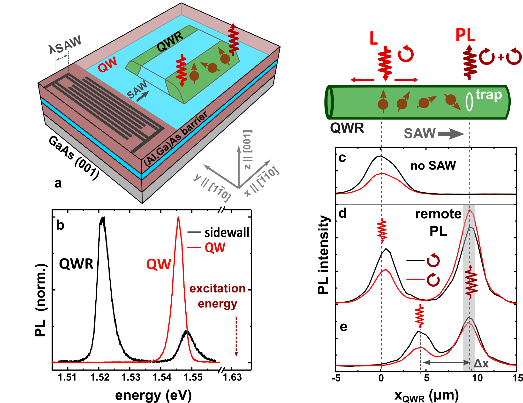
The structure of the QWR samples is illustrated in Fig. 2(a). As described in the Methods section, the GaAs QWRs are fabricated by combining steps of surface patterning and overgrowth by molecular beam epitaxy (MBE). In this process, the growth of an (Al,Ga)As/GaAs/(Al,Ga)As QW stack over a patterned ridge leads to the formation of a thicker GaAs region (the QWR) at the ridge sidewalls, which is electrically connected to the QW[30]. The photoluminescence features of the sample are summarized in Fig. 2(b). Here, the red and black curves compare PL spectra recorded under confocal excitation and detection on the QW region and on the ridge sidewall (corresponding to the QWR position), respectively. The former shows a single PL line with a linewidth (full-width-at-half-maximum, FWHM) of associated with the electron-heavy hole QW exciton at . The spectrum recorded on the ridge sidewall shows the excitonic emission from the QWR at with a FWHM of together with a second line at (FWHM of 5.4 meV). The latter stems from the QW regions near the QWR, which are slightly thinner than those further from the ridge sidewalls [30]. The energy difference between these two lines yields a lateral confinement energy for electrons (holes) in the QWR of approximately ().
The optical detection of acoustically driven spin transport along the QWR is illustrated in Figs. 2(c)-(e). The experiments were carried out using the geometry depicted in the upper right panel by exciting spins using a right-hand circularly polarized laser beam with energy below the QW resonance. The black and red profiles display the spatial distribution of the integrated PL from the QWR [detection window from to , cf. Fig. 2(a)] with right- and left-hand circular polarizations, respectively. In the absence of a SAW [Fig. 2(c)], the emission is restricted to the regions around the excitation spot and has a net right-hand circular polarization. The PL profiles can be fitted with a Gaussian characterized by a FWHM of . The increased spatial PL spread compared to the size of the laser spot is attributed to the diffusion of the spin polarized carriers along the QWR axis.
Figures 2(d) and 2(e) display the corresponding profiles acquired in the presence of a SAW that captures the spin polarized carriers and transports them to trap centers at m, where the electrons and holes recombine. The trapping and recombination centers are defect regions along the QWR[30]. The trapping mechanism, which leads to emission at the same energy as the QWR, is attributed to carrier capture at centers at the interface between the QW (or QWR) layer and the (Al,Ga)As barrier layers assisted by the transverse component of the SAW piezoelectric field, [30, 31]. These centers can capture carriers of one polarity during one half-cycle of the SAW and release them during the passage of carriers of the opposite polarity in the subsequent SAW half-cycle when reverses its sign. The centers provide efficient recombination centers to stop the transport and monitor the PL polarization. Note that the PL polarization depends on the transport distance changing from right- [Fig. 2(e)] to left-hand circular polarization [Fig. 2(d)] as increases from 5 to 10 m. This is due to the larger precession angle under the SO field accumulated while travelling a longer distance.
Spin precession control
The procedure depicted in Figs. 2(c)-(e) was applied to determine the spatial dependence of the spin polarization on the SAW amplitude. The panels of Fig. 3 summarize profiles for acoustic transport in three geometries, which are illustrated in the corresponding upper panels: (a) along the QW, (b) along the QWR and (c) using DQDs. For the QW and QWR, the transport distance is along the -direction, but it is along the -direction for the DQDs. In all cases, oscillates with a period that reduces with increasing SAW amplitudes, which demonstrates the operation principle of the acoustic spin gate. In particular, a distinct reversal of the spin polarization can be observed for both the QWR (m) and DQD (m) geometries, with the latter occurring well within the spin coherence length of transport.
The solid lines are fits of the experimental data to an exponentially decaying cosine function of the form
| (1) |
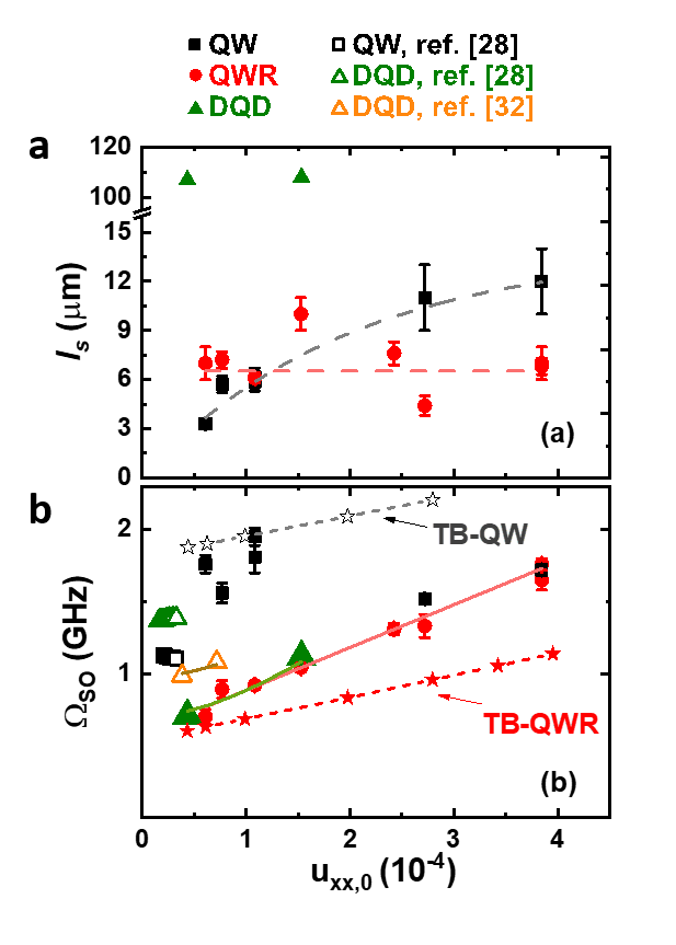
The fit parameters are the total SO angular precession frequency as well as the characteristic spin transport length . can be expressed in terms of the oscillation period . The fit parameters and are displayed as filled symbols in Fig. 4 as a function of the SAW amplitude (stated in terms of the amplitude of the uniaxial strain component , see definition below). For the QWR (solid red dots), m is independent of the SAW amplitude, and this value is equal to the one measured in the absence of a SAW111see Supplemental Material, Sec. SM2 at URL for details about the determination of the spin transport length. In contrast, for the QW (solid black squares) increases with SAW power [cf. Fig. 4(a)]–a behaviour which will be further addressed below. For the DQDs (solid green triangles), is considerably larger and comparable to the maximum measured transport distance.
A further remarkable result is the strong dependence of on the SAW amplitude [cf. Fig. 4(b)] for transport both along the QWRs and by DQDs. These structures thus act as acoustically controlled spin logic and polarization modulators, where the gate is determined by the acoustic amplitude. Their behaviour contrasts with that of the QW data as well as with previous acoustic transport studies of QWs and DQD on thinner QWs (open symbols in Fig. 4 [29, 21]), where the SAW-induced changes in are typically less than 10%.
SAW-related spin-orbit fields
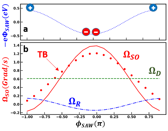
In order to quantify the SO fields induced by the SAW, we first note that the strain field of a Rayleigh SAW along consists of two uniaxial strain components and as well as a phase-shifted shear component [33]. Here, is the QW growth axis, is the SAW phase, and and are the SAW wave vector and angular frequency, respectively. During transport, the SAW piezoelectric potential captures electrons around the SAW phase [cf. Fig. 5(a)] with a strain field (), where they are also subjected to a transverse piezoelectric field proportional to 222see Supplemental Material, Sec. SM5 at URL for details about the contributions of the SAW strain fields to the spin-orbit interaction.
The lateral dimensions of the QWRs and DQDs are much larger than the QWR (or QW) thickness. For the determination of the in QWRs and DQDs, we will neglect the role of the lateral confinement (and of the lateral interfaces) and assume that is essentially equal to the one in a QW of the same thickness. We now address the different SO mechanisms acting on spins acoustically transported along the -direction of a QW with the SAW velocity . The effective electron wave vector is determined by the effective electron mass ( is the reduced Planck’s constant)333see Supplemental Material, Sec. SM3 at URL for details about the contributions of the SAW strain fields to the spin-orbit interaction. The bulk inversion asymmetry (BIA) of the III-V lattice induces an intrinsic SO field (the Dresselhaus term[36]), which leads to the precession of the moving spins with an angular frequency . Here, denotes the extension of the electron wave function along . The structural inversion asymmetry (SIA) induced by the SAW gives rise to precession components related to the strain field, [20], as well as to piezoelectric field , . The terms , , and are material parameters quantifying the strength of the different SO contributions (cf. Sec. SM3). The previous expressions can be combined such that the spin precession frequency for transport by a single SAW beam () and by DQDs () can be stated as: [20, 21]
| (2) | |||||
| (3) |
In Eq. (3), and are the unit vectors parallel and perpendicular to the DQD propagation while and refer to precession frequencies for a single SAW beam along . The term in this equation arises from the fact that the propagation velocity of the DQDs equals to the vector sum of the velocities of the individual SAW beams.
Since (hence ), Eq. (2) predicts a linear dependence of on the SAW amplitude. For a quantitative comparison, we first note that while the [29] and = - [20] have well-established values, the reported values of the strain-related parameter span a wide range (e.g., from in n-type doped bulk GaAs [24, 26] to in a GaAs(001) QW [27]).
The red solid line in Fig. 4(b) is a fit of the QWR data to Eq. (2) and is then used to determine (details in Sec. SM5). While larger than previously reported values, this value reproduces very well the measured data for DQDs (after considering the scaling of due to the larger ) and shows more reasonable agreement with the dashed lines in Fig. 4(b) from tight-binding calculations. The relative signs of the terms of Eq. (2) is also consistent with the distinctive slope of the red solid line in Fig. 4(b). These terms assumed that the electron spins were experiencing the maximum as calculated in Fig. 5(b), which supports the assumption that the electrons have a phase purity near .
Tight-binding calculations of the spin splittings
In order to verify the predictions of the analytical model, we have also calculated the SO field in QWs using the tight-binding (TB) method [37, 38]. The dots in Fig. 5(b) display the dependence on calculated for the QWR under W/m. In the TB calculations, the QWRs were modelled as a thicker QW, thus neglecting the effects of the weak lateral confinement. The total SO component oscillates around an average value following the harmonic dependence of the SAW fields. To compare with the experiments, we further assume that the electrons are stored around the phases of minimum electronic piezoelectric energy , as illustrated in Fig. 5(a). The SAW amplitude dependence of at these phases calculated by the TB method is displayed by the ’s in Fig. 4(b) for the QWR and QW widths. The calculated linear dependence of on strain amplitude, which corresponds to the parameter in Eq.(2), does not depend on the thickness of the structures and is, thus, similar for the QW and QWR. The sign of the parameter determined by the TB method agrees with the experiments, thus reproducing the increase of the precession rate with SAW amplitude. Its magnitude eVnm is slightly (33%) smaller than the experimentally determined one, but still well above previously published experimental values.

Dimensionality effects on the spin dynamics
One interesting observation in connection with Figs. 4 and 5(b) is that the spin transport lengths in the QWRs are much shorter than the ones in the DQDs, despite the much smaller lateral confinement dimensions in the former structures. To understand the impact of the lateral confinement and motional narrowing effects on the spin dynamics, we have carried out Monte-Carlo simulations of the acoustic spin transport for channels with different widths . The results are summarized in Fig. 6. As expected from motional narrowing in the regime of 1D spin transport (), increases with decreasing channel width as with [13]. In addition, we observe similar dependencies of on the channel width for BIA and SIA SO fields.
By using m (as for the QW in Fig. 4), the enclosure of electrons in DQDs defined by m should increase by a factor of . Such a mechanism qualitatively explains the long spin transport lengths by DQDs. It also predicts huge spin lifetimes and transport lengths for the QWRs, which are, however, not observed in the experiments. A possible explanation lies on the nature of the lateral confinement potential: while purely electrostatic for DQDs, it is imposed by structural interfaces in the QWRs. Spin dephasing due to frequent scattering events at these interfaces (known as Elliot-Yafet processes[39]), as previously postulated for QWRs,[14, 40] as well as interface-related SO fields may thus limit in structural channels.
A further remarkable experimental result is the weak SAW amplitude dependence of the spin precession rate for transport in QW structures as compared to QWRs and DQDs [cf. Figs. 4(a) and 5(a)]. This behaviour in QWs also contrasts with the TB predictions as well as with the model leading to Eq. (2). Furthermore, it is at odds with the Monte-Carlo simulations illustrated in Fig. 6(b), which yield the dependence of the spin precession length on channel width. Here, is the ratio between the precession frequencies in a channel with finite width to the one in an unconstrained channel. One finds that is essentially independent of the channel width. This result, which applies for SO fields of both BIA and SIA symmetries, can be qualitatively understood by taking into account that the spin precession rate along the SAW propagation direction () is determined by the carrier velocity component along , which remains equal to the SAW velocity as the carriers diffuse in the lateral direction 444see Supplemental Material, Sec. SM6 at URL for details about the dependence of the precession rate determined by the Monte-Carlo simulations on the channel width.
We now briefly address a mechanism that can account for the weak dependence of on SAW amplitude observed for the QW. This mechanism is based on fluctuations in the storage phase of the carriers in the SAW potential during the transport. The driving force for this transport is the longitudinal component of the SAW piezoelectric field given by . In the previous sections, we have assumed that the electron spins remain at the SAW phase corresponding to the minimum of the piezoelectric energy , as illustrated in Fig. 5(a). At these phases, however, vanishes. To sustain a steady-state motion at the SAW velocity, both electrons (superscript ) and holes () must concentrate around a phase () of the SAW potential satisfying [rather than at , cf. Fig. 5(a)]. At these phases, the SAW-induced SO fields are reduced by a factor with respect to their maximum at . As a result, the effective spin precession frequency reduces and becomes dependent on the effective carrier mobility. Due to the narrower thickness , the transport mobility in the QWs is expected to be lower than in the QWR and DQD cases (the ambipolar mobility scales with in undoped QWs [42]), thus reducing the SAW-induced SO fields relative to the Dresselhaus contribution. As mentioned in connection with Fig. 4(a), increases with SAW power for the spins in the QW, thus indirectly indicating a connection between the mobility and the spin dynamics. According to this mechanism, the lower efficiency of the spin gates in the QW arises from the lower ambipolar mobility relative to the QWR and the DQDs due to its smaller thickness. Further studies are, however, required to quantify the impact of this effect.
III Discussion
In this work, we have demonstrated the ability to acoustically transport and, simultaneously, control the polarization of electrons spins stored within moving potential dots defined by SAWs in GaAs QWs and QWRs. Within the flying control gates, the spins precess around a SAW-induced SO field, and the precession rate can be dynamically changed by a factor of over 2.5 by varying the SAW amplitude, which enabled the controlled flip of the spin polarization. The experimental results for the precession rates markedly exceed previous results and agree well with the predictions of an analytical model for the SAW-induced spin-orbit fields as well as with microscopic tight-binding calculations. The latter of which enable a precise determination of the strain related spin-orbit parameters. We have also addressed the mechanisms governing spin relaxation while considering the role of the carrier mobility and of the lateral interfaces on the spin dynamics. Here, the shorter spin transport lengths measured in structurally defined QWRs as compared to electrostatically defined DQDs are attributed to spin dephasing via frequent scattering at the lateral (Al,Ga)As interfaces. Details of the scattering mechanisms are, however, presently unknown and calls for additional structural studies of the QWR interfaces.
The high degree of dynamical spin control in QWRs and DQDs demonstrated here enables dynamic control by simply changing the acoustic amplitude of the carrier wave. An obvious and important advantage is that both spin transport and manipulation can be performed through this flying spin gate in a single structure (e.g., a QWR) without requiring extra components (e.g., electrostatic gates for Rashba spin control). The experiments in Fig. 3(b) directly illustrate an electro-optical polarization modulators based on this approach. Here, the circular polarization of the PL can be set to an arbitrary value by simply varying the SAW amplitude. This functionality can be naturally extended to the transport of single spins[22] as well as for the generation of polarized single photons[15], thus enabling the realization of a spin-based quantum information processor with a photonic interface.
IV Methods
QWR Sample Fabrication
The planar QWRs used in this work were fabricated using MBE by overgrowing a 10 nm-thick QW on a GaAs(001) substrate pre-patterned with shallow (approximately 30 nm high) rectangular ridges [cf. Fig. 2(a)] [30]. The anisotropic nature of the MBE growth induces a local thickening of the QW at the ridge sidewalls oriented along the -direction along the surface, thus forming a QWR parallel to this sidewall. The thickness and width of the QWR are and , respectively, as determined by scanning transmission electron microscopy [30]. The moving potential dots for carrier and spin transport are created by propagating a SAW with a wavelength m (frequency of MHz at and velocity m/s) along the wire axis. The SAW is generated by a split-finger interdigital transducer deposited on the sample surface. Its amplitude will be quantified in terms of the linear acoustic power density , defined as the ratio between the coupled acoustic power and the width of the SAW beam. During the acoustic transport, the carriers are confined within dots with dimensions equal to the QWR width and less than along the directions perpendicular and parallel to the SAW propagation, respectively. Acoustic spin transport was also investigated in the QW embedding the QWR. In this case, carrier motion is unconstrained in the direction perpendicular to the transport.
DQD Sample Fabrication
The DQDs were created via the interference of two orthogonal SAW beams propagating along the and directions of a 30 nm thick QW on GaAs(001) [15]. The interference of the piezoelectric fields of the SAWs creates an array of DQDs propagating along the surface direction [15]. DQDs yield the longest, so far, reported acoustic spin transport distances [15, 43]. SAWs with a wavelength of m were used and yield DQDs with dimensions of approximately propagating with a velocity 4115 m/s.
Photoluminescence measurements
The spectroscopic photoluminescence (PL) studies of the spin transport were performed at low temperatures (10-20 K) in a microscopic PL setup with radio-frequency (rf) wiring for SAW excitation. The spins were optically excited using a circularly polarized laser beam with tunable wavelength ( between 760 and 808 nm) focused onto a m wide spot on the sample surface. The PL emitted along the SAW path with left- () and right-hand () circular polarization was collected with spatial resolution and used to determine the spin polarization [44] 555see Supplemental Material, Sec. SM1 at URL for further details about the experimental determination of the spin polarization. Since hole-spin relaxation in QWs and QWRs is typically much faster than the one for electrons [46], essentially reflects the electron spin dynamics.
Tight-binding Calculations
The analytical model for the SO fields applies for a QW with infinite potential barriers and, thus, neglects the effects of the QW interfaces. In addition, the model neglects the impact of the SAW field on the electronic states, which can be significant for the valence band states in wide QWs [47]. The the SO field contributions were calculated in QWs using the tight-binding (TB) method [37, 38]. The effects of the SAW were taken into account by using the strain and piezoelectric fields to determine the atomic positions and on-site potentials, respectively, within the TB supercell 666see Supplemental Material, Sec. SM4 at URL for further details about the tight-binding calculation procedure.
Monte Carlo spin dynamics
In the calculations, the spins are assumed to move along the -direction with the SAW velocity while having a random motion along the -direction with mean-free-path and thermal velocity defined by the electron mobility and temperature 777see Supplemental Material, Sec. SM6 at URL for details about the Monte-Carlo simulations. Figure 6(a) and (b) display the simulated dependence of and for transport in channels with different widths under BIA and SIA SO fields. The SO fields were assumed to have an amplitude dictated by a spin precession period m similar to the ones measured for QWs in Fig. 3. We further assumed and K, which yield m.
V Author Contributions
P.L.J.H. performed the experiments and analysis on the QW and QWR samples, and J.A.H.S. performed the experiments and analysis using the DQDs. K.B. performed the MBE growth of the samples. Initial discussions and experimental design and development between H.S., Y.K., and P.L.J.H. were critical inputs to the presented results. P.V.S. led the theory calculations and supervised the project. P.L.J.H., P.V.S., and J.A.H.S. wrote the manuscript with input from the other authors.
Acknowledgements.
We thank S. Ludwig for discussions and for a critical reading of the manuscript, A.C. Poveda for the help with the graphics, as well as S. Rauwerdink for the help in the fabrication of the samples. J. Stotz would also like to acknowledge the Natural Science and Engineering Research Council of Canada and the Alexander von Humboldt Foundation. This project has received funding from the European Union’s Horizon 2020 research and innovation program under grant agreement No 642688.References
- Datta and Das [1990] S. Datta and B. Das, Electronic analog of the electro-optic modulator, Appl. Phys. Lett. 56, 665 (1990).
- Bychkov and Rashba [1984] Y. A. Bychkov and E. I. Rashba, Oscillatory effects and the magnetic susceptibility of carriers in inversion layers, J. Phys. C 17, 6039 (1984).
- Koo et al. [2009] H. C. Koo, J. H. Kwon, J. Eom, J. Chang, S. H. Han, and M. Johnson, Control of spin precession in a spin-injected field effect transistor, Science 325, 1515 (2009).
- Chuang et al. [2015] P. Chuang, S.-C. Ho, L. W. Smith, F. Sfigakis, M. Pepper, C.-H. Chen, J.-C. Fan, J. P. Griffiths, I. Farrer, H. E. Beere, G. A. C. Jones, D. A. Ritchie, and T.-M. Chen, All-electric all-semiconductor spin field-effect transistors, Nat. Nanotechnol. 10, 35 (2015).
- D’yakonov and Perel’ [1971] M. I. D’yakonov and V. I. Perel’, Spin orientation of electrons associated with the interband absorption of light in semiconductors, SPJETP 33, 1053 (1971).
- Ohno et al. [1999] Y. Ohno, R. Terauchi, T. Adachi, F. Matsukura, and H. Ohno, Spin relaxation in GaAs(110) quantum wells, Phys. Rev. Lett. 83, 4196 (1999).
- Hernández-Mínguez et al. [2012] A. Hernández-Mínguez, K. Biermann, R. Hey, and P. V. Santos, Electrical suppression of spin relaxation in GaAs(111)B quantum wells, Phys. Rev. Lett. 109, 266602 (2012).
- Bernevig et al. [2006] B. A. Bernevig, J. Orenstein, and S.-C. Zhang, Exact SU(2) symmetry and persistent spin helix in a spin-orbit coupled system, Phys. Rev. Lett. 97, 236601 (2006).
- Koralek et al. [2009] J. D. Koralek, C. P. Weber, J. Orenstein, B. A. Bernevig, S.-C. Zhang, S. Mack, and D. D. Awschalom, Emergence of the persistent spin helix in semiconductor quantum wells, Nature 458, 610 (2009).
- Walser et al. [2012] M. P. Walser, C. Reichl, W. Wegscheider, and G. Salis, Direct mapping of the formation of a persistent spin helix, Nat. Phys. 8, 757 (2012).
- Balocchi et al. [2011] A. Balocchi, Q. H. Duong, P. Renucci, B. L. Liu, C. Fontaine, T. Amand, D. Lagarde, and X. Marie, Full electrical control of the electron spin relaxation in GaAs quantum wells, Phys. Rev. Lett. 107, 136604 (2011).
- Kikkawa and Awschalom [1999] J. M. Kikkawa and D. D. Awschalom, Lateral drag of spin coherence in gallium arsenide, Nature 397, 139 (1999).
- Kiselev and Kim [2000] A. A. Kiselev and K. W. Kim, Progressive suppression of spin relaxation in two-dimensional channels of finite width, Phys. Rev. B 61, 13115 (2000).
- Holleitner et al. [2006] A. W. Holleitner, V. Sih, R. C. Myers, A. C. Gossard, and D. D. Awschalom, Suppression of spin relaxation in submicron InGaAs wires, Phys. Rev. Lett. 97, 036805 (2006).
- Stotz et al. [2005] J. A. H. Stotz, R. Hey, P. V. Santos, and K. H. Ploog, Coherent spin transport via dynamic quantum dots, Nat. Mater. 4, 585 (2005).
- Sanada et al. [2013] H. Sanada, Y. Kunihashi, H. Gotoh, K. Onomitsu, M. Kohda, J. Nitta, P. V. Santos, and T. Sogawa, Manipulation of mobile spin coherence using magnetic-field-free electron spin resonance, Nat. Phys. 9, 280 (2013).
- Rocke et al. [1998] C. Rocke, A. O. Govorov, A. Wixforth, G. Böhm, and G. Weimann, Exciton ionization in a quantum well studied by surface acoustic waves, Phys. Rev. B 57, R6850 (1998).
- Maialle et al. [1993] M. Z. Maialle, E. A. de Andrada e Silva, and L. J. Sham, Exciton spin dynamics in quantum wells, Phys. Rev. B 47, 15776 (1993).
- Sogawa et al. [2001] T. Sogawa, P. V. Santos, S. K. Zhang, S. Eshlaghi, A. D. Wieck, and K. H. Ploog, Transport and lifetime enhancement of photoexcited spins in GaAs by surface acoustic waves, Phys. Rev. Lett. 87, 276601 (2001).
- Hernández-Mínguez et al. [2014] A. Hernández-Mínguez, K. Biermann, R. Hey, and P. V. Santos, Spin transport and spin manipulation in (110) and (111) GaAs quantum wells, Phys. Status Solidi B 251, 1736 (2014).
- Sanada et al. [2011] H. Sanada, T. Sogawa, H. Gotoh, K. Onomitsu, M. Kohda, J. Nitta, and P. V. Santos, Acoustically induced spin-orbit interactions revealed by two-dimensional imaging of spin transport in GaAs, Phys. Rev. Lett. 106, 216602 (2011).
- Bertrand et al. [2016] B. Bertrand, S. Hermelin, S. Takada, M. Yamamoto, S. Tarucha, A. Ludwig, A. D. Wieck, C. Bäuerle, and T. Meunier, Fast spin information transfer between distant quantum dots using individual electrons, Nat. Nanotechnol. 11, 672 (2016).
- D’yakonov et al. [1979] M. I. D’yakonov, I. A. Merkulov, and V. I. Perel’, Optical-orientation anisotropy produced in semiconductors by quadrupole splitting of the spin levels of the lattice nuclei, SPJETP 49, 160 (1979).
- Pikus et al. [1988] G. E. Pikus, V. A. Marushchak, and A. N. Titkov, Spin splitting of energy bands and spin relaxation of carriers in cubic III-V crystals (review), Sov. Phys. Semicond. 22, 115 (1988).
- Kato et al. [2004] Y. Kato, R. C. Myers, A. C. Gossard, and D. D. Awschalom, Coherent spin manipulation without magnetic fields in strained semiconductors, Nature 427, 50 (2004).
- Beck et al. [2006] M. Beck, C. Metzner, S. Malzer, and G. H. Doehler, Spin lifetimes and strain-controlled spin precession of drifting electrons in zinc blende type semiconductors, Europhys. Lett. 75, 597 (2006).
- English et al. [2011] D. J. English, P. G. Lagoudakis, R. T. Harley, P. S. Eldridge, J. Hübner, and M. Oestreich, Strain-induced spin relaxation anisotropy in symmetric (001)-oriented GaAs quantum wells, Phys. Rev. B 84, 155323 (2011).
- Biermann et al. [2010] K. Biermann, O. D. D. Couto, Jr., E. Cerda, H. B. de Carvalho, R. Hey, and P. V. Santos, Spin transport in (110) GaAs-based cavity structures, J. Supercond. Novel Magn. 23, 27 (2010).
- Stotz et al. [2006] J. A. H. Stotz, R. Hey, P. V. Santos, and K. H. Ploog, Spin transport and manipulation by mobile potential dots in GaAs quantum wells, Physica E 32, 446 (2006).
- J.Helgers et al. [2019] P. L. J.Helgers, H. Sanada, Y. Kunihashi, A. Rubino, C. Christopher J. B. Ford, K. Biermann, and P. V. Santos, Sidewall quantum wires on GaAs (001) substrates, Phys. Rev. Applied 11, 064017 (2019).
- Lazić et al. [2012] S. Lazić, R. Hey, and P. Santos, Mechanisms for non-classical light emission from acoustically populated (311)A GaAs quantum wires, New J. of Phys. 14, 013005 (2012).
- Note [1] See Supplemental Material, Sec. SM2 at URL for details about the determination of the spin transport length.
- de Lima, Jr. and Santos [2005] M. M. de Lima, Jr. and P. V. Santos, Modulation of photonic structures by surface acoustic waves, Rep. Prog. Phys. 68, 1639 (2005).
- Note [2] See Supplemental Material, Sec. SM5 at URL for details about the contributions of the SAW strain fields to the spin-orbit interaction.
- Note [3] See Supplemental Material, Sec. SM3 at URL for details about the contributions of the SAW strain fields to the spin-orbit interaction.
- Dresselhaus [1955] G. Dresselhaus, Spin-orbit coupling effects in zinc blende structures, Phys. Rev. 100, 580 (1955).
- Santos and Cardona [1994] P. V. Santos and M. Cardona, Comment on: Observation of spin precession in GaAs inversion layers using antilocalization, Phys. Rev. Lett. 72, 432 (1994).
- Santos et al. [1995] P. V. Santos, M. Willatzen, M. Cardona, and A. Cantarero, Tight-binding calculations of spin splittings in semiconductor superlattices, Phys. Rev. B 51, 5121 (1995).
- Elliott [1954] R. J. Elliott, Theory of the effect of spin-orbit coupling on magnetic resonance in some semiconductors, Phys. Rev. 96, 266 (1954).
- Alsina et al. [2008] F. Alsina, J. A. H. Stotz, R. Hey, U. Jahn, and P. V. Santos, Acoustic charge and spin transport in GaAs quantum wires, Phys. Status Solidi C 9, 2907 (2008).
- Note [4] See Supplemental Material, Sec. SM6 at URL for details about the dependence of the precession rate determined by the Monte-Carlo simulations on the channel width.
- Vörös et al. [2005] Z. Vörös, R. Balili, D. W. Snoke, L. Pfeiffer, and K. West, Long-distance diffusion of excitons in double quantum well structures, Phys. Rev. Lett. 94, 226401 (2005).
- Stotz et al. [2008] J. A. H. Stotz, P. V. Santos, R. Hey, and K. H. Ploog, Mesoscopic spin confinement during acoustically induced transport, New J. Phys. 10, 093013 (2008).
- Dyakonov [2008] M. I. Dyakonov, Spin physics in semiconductors (Springer, 2008).
- Note [5] See Supplemental Material, Sec. SM1 at URL for further details about the experimental determination of the spin polarization.
- Baylac et al. [1995] B. Baylac, X. Marie, T. Amand, M. Brousseau, J. Barrau, and Y. Shekun, Hole spin relaxation in intrinsic quantum wells, Surf Sci 326, 161 (1995).
- Santos et al. [2004] P. V. Santos, F. Alsina, J. A. H. Stotz, R. Hey, S. Eshlaghi, and A. D. Wieck, Band mixing and ambipolar transport by surface acoustic waves in GaAs quantum wells, Phys. Rev. B 69, 155318 (2004).
- Note [6] See Supplemental Material, Sec. SM4 at URL for further details about the tight-binding calculation procedure.
- Note [7] See Supplemental Material, Sec. SM6 at URL for details about the Monte-Carlo simulations.