Nanoscale Texture and Microstructure in NdFeAs(O,F)/IBAD-MgO Superconducting Thin Film with Superior Critical Current Properties
Abstract
This paper reports the nanoscale texture and microstructure of a high-performance NdFeAs(O,F) superconducting thin film grown by molecular beam epitaxy on a textured MgO/\chY2O3/Hastelloy substrate. The NdFeAs(O,F) film forms a highly textured columnar grain structure by epitaxial growth on the MgO template. Although the film contains stacking faults along the -plane as well as grain boundaries perpendicular to the -plane, good superconducting properties are measured: a critical temperature, , of 46 K and a self-field critical current density, , of at 4.2 K. Automated crystal orientation mapping by scanning precession electron diffraction in transmission electron microscopy is employed to analyze the misorientation angles between adjacent grains in a large ensemble (247 grains). 99% of the grain boundaries show in-plane misorientation angles () less than the critical angle , which satisfies one of the necessary conditions for the high . Comparing the columnar grain size distribution with the mean distance of the flux line lattice, the triple junctions of low-angle grain boundaries are found to be effective pinning centers, even at high temperatures ( K) and/or low magnetic fields.
keywords:
Fe-based superconductor, epitaxial thin film, nanoscale textural characterization, triple junction, in-plane / out-of-plane misorientationsKyushu University Chikushi] Department of Applied Science for Electronics and Materials, Kyushu University, Fukuoka 816-8580, Japan \alsoaffiliation[CREST Japan] Core Research for Evolutionary Science and Technology, Japan Science and Technology Agency, Tokyo 102-0076, Japan Kyushu University URC] The Ultramicroscopy Research Center, Kyushu University, Fukuoka 819-0395, Japan Nagoya University] Department of Materials Physics, Nagoya University, Nagoya 464-8603, Japan Nagoya University] Department of Materials Physics, Nagoya University, Nagoya 464-8603, Japan \alsoaffiliation[CREST Japan] Core Research for Evolutionary Science and Technology, Japan Science and Technology Agency, Tokyo 102-0076, Japan Nagoya University] Department of Materials Physics, Nagoya University, Nagoya 464-8603, Japan \alsoaffiliation[CREST Japan] Core Research for Evolutionary Science and Technology, Japan Science and Technology Agency, Tokyo 102-0076, Japan Karlsruhe Institute of Technology] Institute for Technical Physics, Karlsruhe Institute of Technology, Hermann-von-Helmholtz-Platz 1, 76344 Eggenstein-Leopoldshafen, Germany Nagoya University] Department of Materials Physics, Nagoya University, Nagoya 464-8603, Japan Kyushu University Chikushi] Department of Applied Science for Electronics and Materials, Kyushu University, Fukuoka 816-8580, Japan \alsoaffiliation[CREST Japan] Core Research for Evolutionary Science and Technology, Japan Science and Technology Agency, Tokyo 102-0076, Japan \alsoaffiliation[Kyushu University URC] The Ultramicroscopy Research Center, Kyushu University, Fukuoka 819-0395, Japan \alsoaffiliationDepartment of Advanced Materials Science and Engineering, Faculty of Engineering Sciences, Kyushu University, Fukuoka 816-8580, Japan
1 Introduction
Since the discovery of Fe-based superconductors (FBS),1 fundamental properties and possibilities for applications of them have been investigated intensively. Among FBSs, FeAs(O,F) () show the highest superconducting transition temperature, (up to around 58 K)2, which is advantageous for applications because of a large margin between and the operating temperatures, e.g. those a cryocooler can reach. Additionally, the theoretical limit of the critical current density (i.e., depairing current density for which Cooper pairs are separated by kinetic energy) is around 170 MA/cm2 at zero kelvin,3 which is the highest value among FBSs. Enhancing the of polycrystalline FeAs(O,F) makes this material more attractive for applications.4 However, polycrystalline FeAs(O,F) generally does not show the best performance, because significantly decreases in the presence of high-angle grain boundaries (HAGB) with misorientation angles larger than the critical angle , for which inter-grain starts to decrease exponentially. Hence, these HAGBs become serious weak links.5, 6 In our previous study,7 was evaluated to be for NdFeAs(O,F) bicrystals with symmetrical [001]-tilt boundaries, which is close to for Co-doped \chBaFe2As2 (Ba-122)8 and Fe(Se,Te) bicrystals.9, 10 Therefore, strict control of the texture is required to fully utilize its potential advantages in applications.
Furthermore, it is promising that the grain boundary engineering can enhance in-field for some superconductors. For example, a P-doped Ba-122 film on a poorly textured polycrystalline MgO template exhibited notably better magnetic flux pinning properties and, therefore, higher values than such a film on a well-textured MgO template.11 This result was explained by a higher density of low-angle grain boundaries (LAGB) in the poorly textured film, which act as pinning centers. This kind of grain boundary pinning was also reported for other superconductors, such as \chMgB2.12 One can therefore presumably take advantage of introducing grain boundaries also in FeAs(O,F) films to pin magnetic flux lines and enhance in-field if grain boundaries are appropriately engineered, i.e. with grain boundary angles predominantly smaller than .
In regard to solving the aforementioned challenge, the film growth of textured NdFeAs(O,F) by molecular beam epitaxy (MBE) on highly textured MgO templates13 has been studied. These templates are prepared by ion-beam-assisted deposition (IBAD) on \chY2O3-buffered Hastelloy tapes.14 IBAD is a typical technique for depositing a biaxially textured film on an untextured metal tape.15 After optimization of various fabrication parameters, the NdFeAs(O,F) thin film exhibited a self-field of at 4.2 K, which is comparable to for single-crystalline NdFeAs(O,F) thin films. Because NdFeAs(O,F) thin films on textured MgO templates are expected to contain a high density of grain boundaries and other defects that influence , it is worthwhile to investigate the microstructure of the NdFeAs(O,F)/IBAD-MgO thin film in fine detail.
In this paper, the microstructure of this NdFeAs(O,F)/IBAD-MgO thin film is analyzed by electron microscopy. Atomic-scale microstructural features and the nanoscale crystal orientation distribution have been evaluated by several TEM and scanning TEM (STEM) techniques. Especially, automated crystal orientation mapping (ACOM) using scanning precession electron diffraction (SPED, see also Supporting Information (SI)) has revealed quantitative and quasi-statistical information about the nanoscale texture and microstructure. They are correlated with the macroscopic transport properties: the misorientation angles between neighboring grains compared with as well as the grain size distribution compared with the mean flux line distance. Based on the assessments described above, the essential features of the microstructure are directly correlated to the superior critical current properties of the NdFeAs(O,F)/IBAD-MgO thin film.
2 Results and discussion
2.1 Crystal structure and global texture
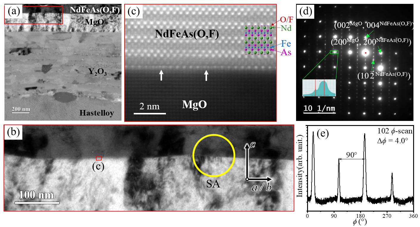
The bright-field TEM image shown in Figure 1a is a cross-sectional view of the film sample. A columnar contrast is observed in both NdFeAs(O,F) and MgO (Figure 1b). The azimuthal -scan of the NdFeAs(O,F) peak obtained by X-ray diffraction (XRD) (Figure 1e) indicates a strong biaxial texture. The average full width at half maximum (FWHM) of the peaks, , is well below . The epitaxial relationship as confirmed by electron diffraction (Figure 1d) is . Additionally, the atomic-resolution annular dark-field (ADF) STEM image (Figure 1c) clearly exhibits the layered atomic structure of the NdFeAs(O,F) film: the FeAs conductive layers and the Nd(O,F) charge-reservoir layers alternate along the crystallographic direction. The white arrows point out misfit dislocations at the interface, which relieve the inner stress induced by lattice mismatch between NdFeAsO ( nm)16 and MgO ( nm)17.
2.2 Grain size distribution
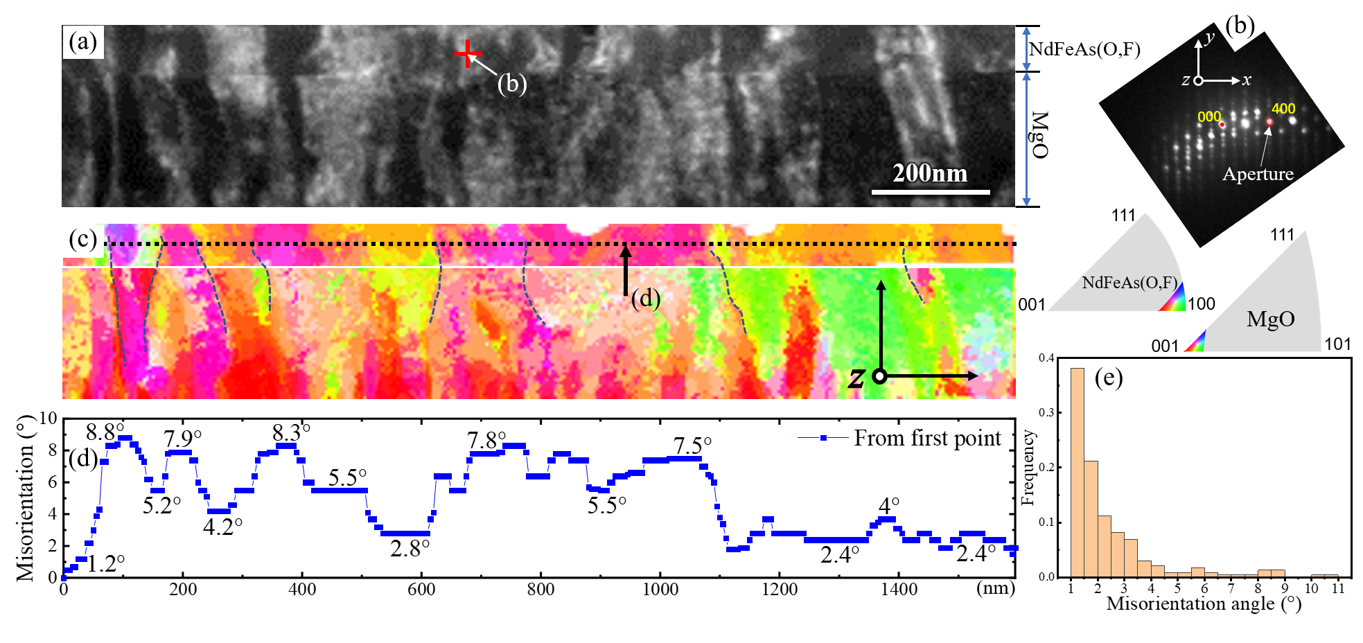
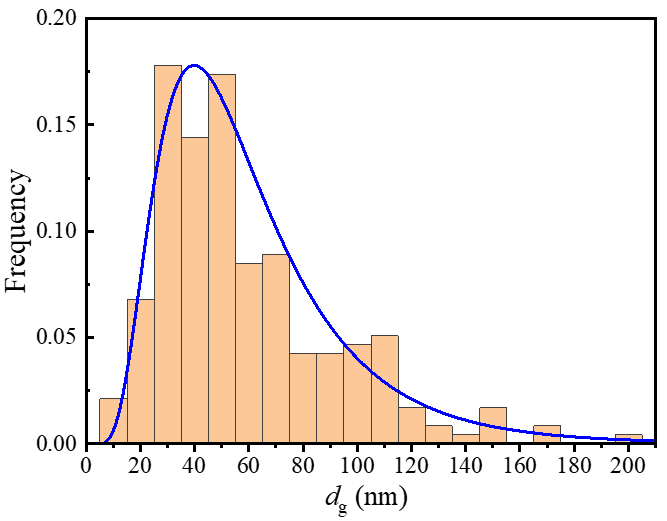
Figure 2a shows a virtual dark-field TEM image of the NdFeAs(O,F) film and the MgO template exported from an SPED data set using the intensity distribution at the diffraction spot (Figure 2b). A nearly vertical stripe contrast is recognized in both NdFeAs(O,F) and IBAD-MgO, which is continuously connected between the two phases. This image contrast indicates the texture transfers from the MgO template to the NdFeAs(O,F) film, and thus, the texture of the film can be engineered by this kind of technical substrates. The nanoscale crystal orientation map in Figure 2c (see also Figure S2 in SI) shows the distribution of strongly -axis correlated grain boundaries and the texture in great detail, revealing a wide distribution of grain sizes (about 20–120 nm). Figure 2d shows a typical misorientation angle profile along the dotted line in the NdFeAs(O,F) film in Figure 2c, which was calculated between each data point and the left-edge point on the line. This method enables us to measure precisely the misorientation angle between adjacent grains, , and the distance between adjacent grain boundaries, . Figure 2e shows the distribution of calculated from 247 grains acquired from ten random cross-sectional foil samples. These values are very small and show a highly compact distribution (peaked at about ), which means that the majority of the grain boundaries in NdFeAs(O,F) are LAGBs or sub-GBs. In addition, the distribution of measured from 247 grains, Figure 3, shows a mean value of 61 nm, and grains in the range of 30–55 nm account for a large proportion. This will be discussed together with the matching-field effect.
2.3 Superconducting properties
The superconducting transition temperature, , of this highly textured NdFeAs(O,F) film was determined as around 46 K from the magnetization measurement, corresponding to the zero resistivity temperature, as shown in Figure 4a. Upper critical field and irreversibility field were determined from the temperature dependencies of the resistivity - at constant applied fields (Figure 4b,c) and compiled to the corresponding phase diagram (Figure 4d). values evaluated from - measurements (Figure 5a) almost overlap with those from the resistivity. Furthermore, the slope of changes at T (marked by arrow), which indicates the matching-field effect that will be discussed later. Above the matching field, shows a near-linear power law relation
| (1) |
with K and (see also Figure S3a).
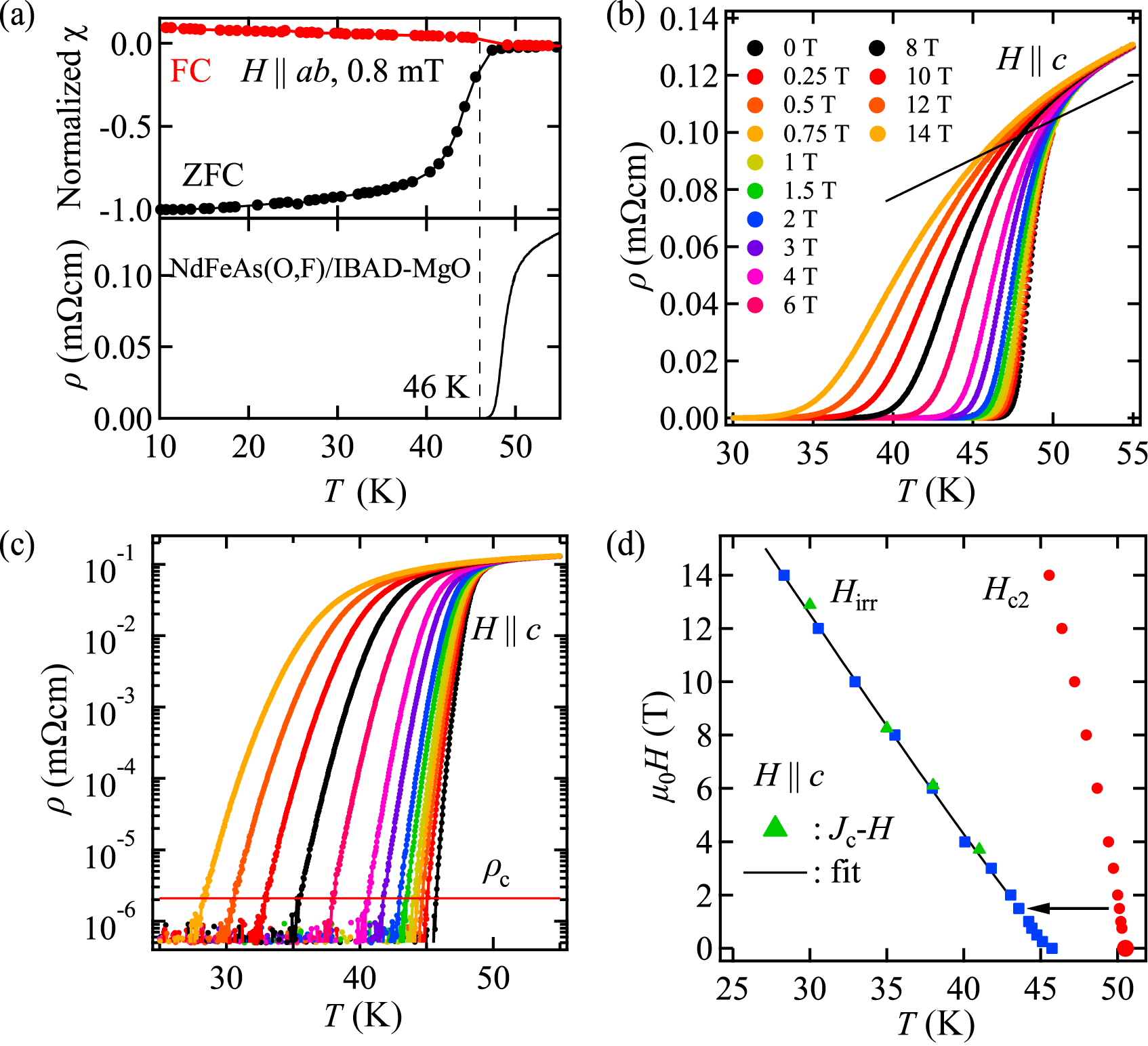
The of this NdFeAs(O,F)/IBAD-MgO film exceeds the required level for applications even at 14 T and 10 K (Figure 5a). The self-field reaches at 4.2 K, which is remarkably higher than previously reported ( at 5 K)13 despite the similar value of for the main texture component of NdFeAs(O,F). This result suggests that the presence of even a small amount of in-plane rotated grains limited in the previous sample due to the erosion of grain boundaries by excess of fluorine. Note that the presence of such rotated grains in Co-doped Ba-122 does not reduce because of the absence of fluorine.18 Figure 5b shows the corresponding pinning force densities as a function of the magnetic field, and Figure 5c,d the same data normalized as vs. , where was estimated from Equation 1 for the lowest temperatures ( K). For K, can be scaled with an exponent of for , which is close to 1. This indicates that point-like core pinning plays an important role for ,19, 20 in the sense of single-occupied defects larger than coherence length . For K, an exponent (close to 0.5) rather describes the data well, indicating that two-dimensional (2D) pinning, e.g. at the LAGBs, governs . This result indicates that the dominant pinning centers or mechanisms change with temperature. As mentioned above, many small columnar grains having a diameter of 30–55 nm in NdFeAs(O,F) provide sufficient LAGBs parallel or nearly parallel to -axis, which can work as effective 2D pinning centers at low temperatures ( K). Aside from those, no point-like pins of size 4–6 nm (considering the temperature dependence of coherence length) were visible in this superconducting film. Consequently, there should be other features that can serve as strong pinning centers at high temperatures (35–41 K).
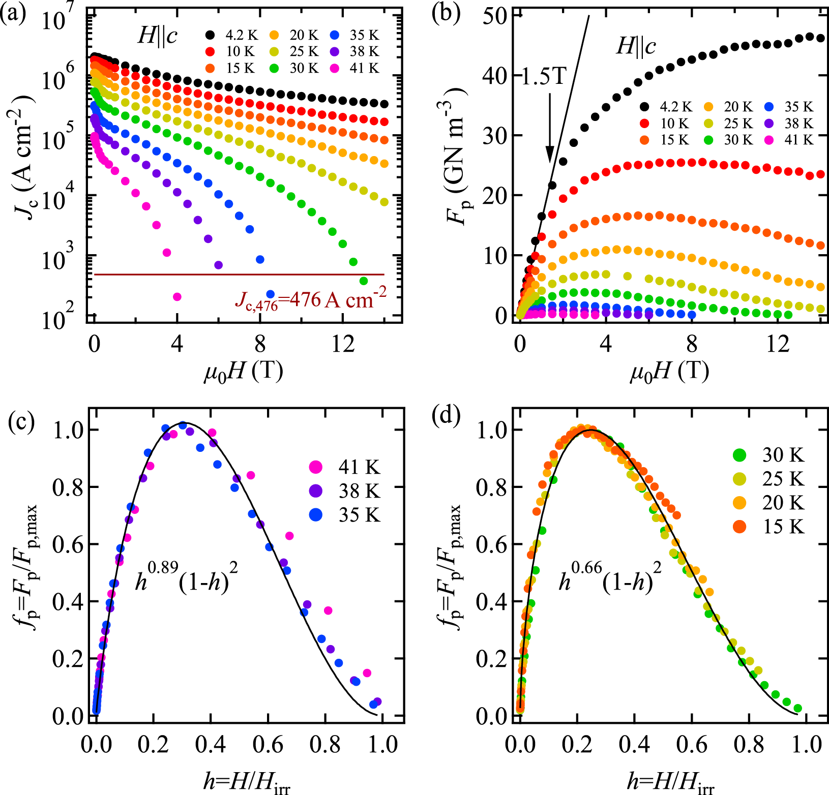
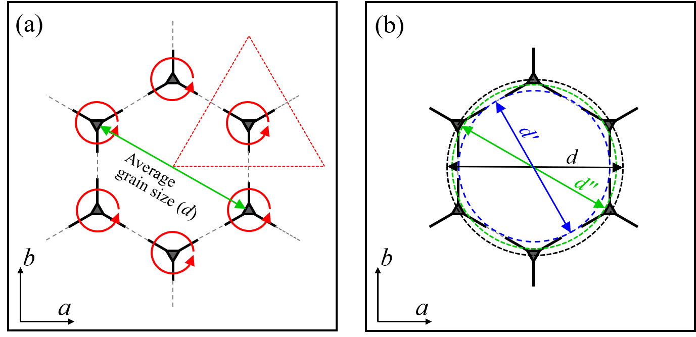
After further investigation, the triple junctions (TJs) of the LAGBs were expected to act as effective pinning centers with a larger transverse dimension for fields of , which provide stronger pinning forces than LAGBs.21 In the following, this hypothesis will be checked. According to the orientation analysis of the film (Figure 2), the LAGBs of the epitaxial columnar grains are in general randomly distributed, like a low-angle grain boundary network. It has been shown that the edge number probability of grains in sufficiently large netlike 2D systems sharply peaks around 6, i.e. the most likely grain form is a hexagon.22, 23 Due to the columnar grain growth in the NdFeAs(O,F) film on MgO template (Figure 1,2,S2), it is therefore reasonable to model its microstructure solely with hexagonal prismatic grains without loss of generality. In fact, the quasi-hexagonal grain was observed in high-resolution plan-view image of the MgO template (Figure S4). This justifies the validity of our hypothesis, since the texture of MgO template transfers to NdFeAs(O,F). Moreover, a similar structure has been artificially fabricated and analyzed in ref.24. As illustrated in Figure 6a, the mean area per TJ (the red dashed triangle) will be ( is the mean grain area). If the flux lines25 are matched with TJs one by one (depicted by the red circular arrows in Figure 6a), the matching field relational formula will be ( Wb is the elementary flux quantum). Then, when substituting the mean value of for the mean grain diameter, for the three alternative definitions of the hexagonal grain diameter shown in Figure 6b, the corresponding matching fields are calculated as
| (2) |
i.e. the matching field T. The same field can also be recognized in - at low temperature as maximum field of the nearly linear behavior (pointed by the arrow in Figure 5b and Figure S3c), usually marking single vortex pinning. This gives evidence of the stronger pinning effect of triple junctions, even at high temperatures (35–41 K) where the LAGBs and small point-like defects cannot contribute anymore. This leads to a possible explanation for the different values of : At high temperatures, where the field range up to is relatively larger compared to the irreversibility field, vortex pinning is dominated by the TJs. At low temperatures, others, most likely smaller defects such as the LAGBs themselves with occasional dislocations as well as atomic defects, have to come into play because the irreversibility field is now much larger than . Considering that the TJs most likely have a larger transverse dimension than the adjacent LAGBs, this explanation is supported by the results of Paturi et al. on YBCO nanocomposite films with .26 They found that the exponent increases roughly linearly from for defects in the range of value towards for the largest defects at the verge of multi-vortex pinning. The values of 0.66 and 0.89 of our film lay well in this range.
2.4 Angular maps of in-plane and out-of-plane crystal rotation
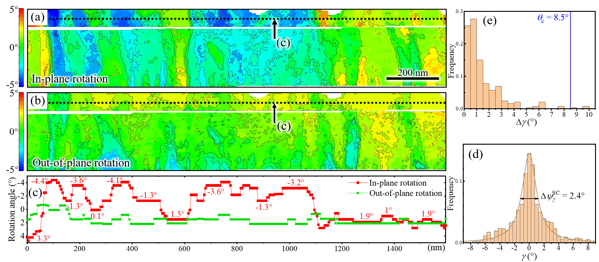
In order to thoroughly investigate in-plane and out-of-plane misorientations separately, crystal rotation angles around the -axis (in-plane rotation angle, ), and around a line within the -plane (out-of-plane rotation angle, ) of each data point were extracted from the Euler angles of crystal orientation mapping data (Figure 2) of the NdFeAs(O,F) film and the MgO template. The detailed extracting method is described in SI (Figure S5) and ref.27, 28. The resultant in-plane and out-of-plane crystal rotation angular maps are shown in Figure 7a,b. The difference between adjacent contour lines is . From the clear color contrast and contour lines in the maps, it is evident that the film crystals’ size and orientation, both in-plane and out-of-plane, are dominated by those of the MgO template, where the orientation distribution slightly broadens in both cases (see Figure S5 in SI). In addition, it is also visualized that the in-plane misorientation is larger than the out-of-plane misorientation in most domains of NdFeAs(O,F) film and MgO template.
Figure 7c shows the angular profiles along the horizontal dotted lines in the NdFeAs(O,F) film indicated in Figure 7a,b. The angular profile of the in-plane rotation is similar to the misorientation angle profile in Figure 2d, while the out-of-plane rotation profile shows a much smaller fluctuation. This feature illustrates again the dominance of the in-plane rotation in the total crystal rotations of this sample. The histogram of the in-plane rotation angle () distribution from all 10 data sets, Figure 7d, is well described by a Lorentz distribution. This enables us to compare the FWHM of this in-plane rotation angle distribution counted from SPED orientation data ( in Figure 7d) with the average FWHM of -scan peaks of XRD of this sample ( in Figure 1e). The reason of is partially ascribed to the fact that the XRD -scan peaks of in-plane reflections also contain contributions of the out-of-plane crystal rotation.29 Furthermore, orientation variations on a larger length scale than measurable by TEM are likely, which contribute to the integral determination in XRD. Besides, the in-plane and out-of-plane rotation angle distributions of the MgO template were also investigated in detail, and can be found in Figure S6.
The in-plane misorientation angles between adjacent grains, , were also calculated and statistically analyzed, as shown in Figure 7e. 99% of all values are smaller than the critical angle regarding the [001]-tilt grain boundary (blue line).
2.5 Microstructural analysis at boundaries and defects
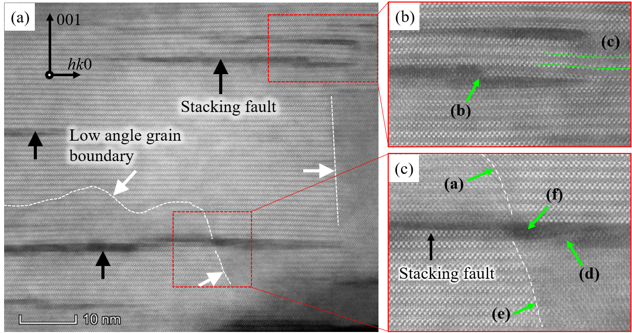
In addition, although the in-plane misorientations are the main component, the small yet present out-of-plane misorientations were also observed. The corresponding histogram to Figure 7e for out-of-plane misorientation angles, , is displayed in Figure S7 of SI. It was found in the layered NdFeAs(O,F) structure that the vertical grain boundaries present three different sorts of conformation: the sole in-plane misorientation (, ), the sole out-of-plane misorientation (, ) and a composite structure of these two states (, ). Some representative diagrams of these three sorts of conformation are sketched in Figure 8. As depicted in Figure 8a, the [001]-tilt grain boundaries with only in-plane misorientation (, ) can be formed without discontinuing the atomic layers of the conductive FeAs and the charge-reservoir Nd(O,F). On the other hand, the grain boundaries with out-of-plane misorientation () display three types of configurations: the []-twist boundary (Figure 8b,e), the []-tilt boundary (Figure 8c) and the mixed state of them (Figure 8d). In particular, the out-of-plane misorientations in Figure 8b,e will cause disconnections of FeAs and Nd(O,F) atomic layers. Accordingly, it may be initially considered that out-of-plane misorientations have a more severe impact on than in-plane misorientations. However, even in the presence of out-of-plane misorientations, the FeAs and Nd(O,F) atomic layers can maintain or restore their continuity at grain boundaries by continuously curving and/or introducing stacking faults, as the structure depicted in Figure 8d,f.
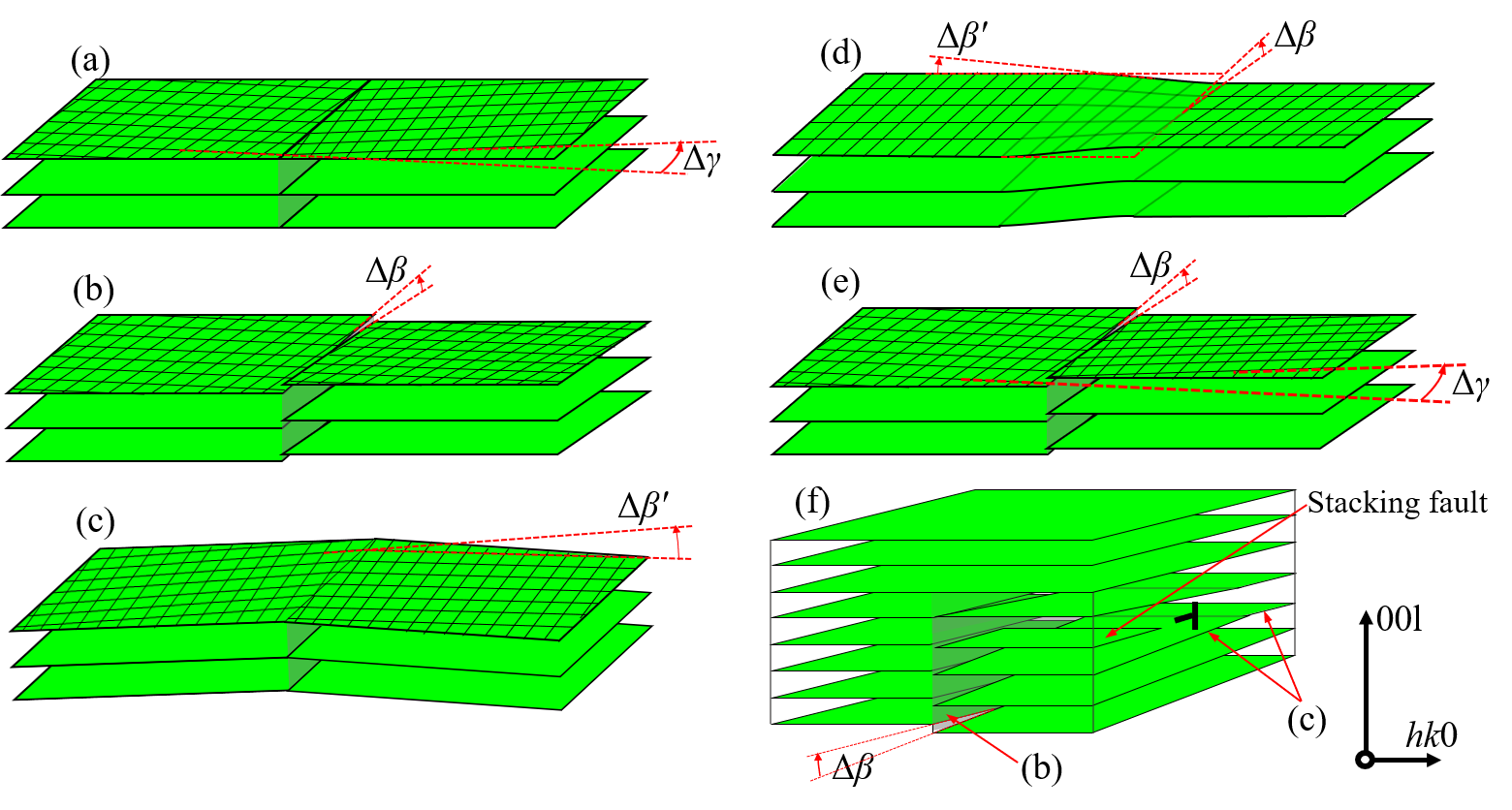
All configurations exhibited in Figure 8 have been observed and pointed out one by one in Figure 9 showing the microstructure on the atomic scale. Moreover, microstructural observations of multiple areas in the ten specimens revealed that the phenomenon of restoring the continuity of atomic layers is universal in this epitaxial NdFeAs(O,F) film. This may be the reason why such a small out-of-plane misorientation did not degrade the of this film apparently. Furthermore, as with the in-plane misorientation, there should also be a critical angle for the out-of-plane misorientation, i.e. . When , most of atomic layers will no longer be able to restore the continuity in grain boundaries. As a result, the dense non-superconducting barriers make the decrease exponentially with .
3 Conclusions
A textured NdFeAs(O,F) thin film grown by MBE on IBAD-MgO substrate exhibited superior superconducting properties: a critical temperature K, self-field up to at 4.2 K, and in-field for of at 10 T, 15 K. The nanoscale crystal orientation mapping using SPED verified the highly textured columnar grain structure, where 99% of in-plane misorientations between adjacent grains were less than of . This demonstrates that the present sample satisfies one of the necessary conditions for high superconducting films. In addition, in the presence of the small out-of-plane misorientations in this epitaxial NdFeAs(O,F) film, the atomic layers can maintain or restore their continuity at grain boundaries by continuously curving and/or introducing stacking faults. As a result, this study supports the effectiveness of grain boundary engineering within for the epitaxial Fe-based superconducting films for high field applications. In addition, the triple junctions of grain boundaries are expected to act as pinning centers, even at high temperatures (35–41 K).
4 Experimental Methods
4.1 Growth of Films and Measurement of Superconducting Properties
The NdFeAs(O,F) thin films were grown on a IBAD-MgO/\chY2O3/Hastelloy substrate by MBE, as described in detail in ref.13. To obtain superconducting films, a NdOF over-layer was deposited on the mother compound (NdFeAsO) for F doping by diffusion.30 The thickness of \chY2O3, MgO and NdFeAsO were 710 nm, 210 nm and 70 nm, respectively, confirmed by TEM. After the film growth, the sample was laser-cut into small pieces for structural analysis and electromagnetic property measurements. The temperature dependence of magnetization was measured by a superconducting quantum interference device (SQUID) magnetometer to determine the superconducting transition temperature under a magnetic field of 0.8 mT parallel to the film’s -plane, . A small bridge of 0.03 mm width and 0.5 mm length was fabricated by laser cutting for electrical transport measurements. To draw the magnetic phase diagram for fields perpendicular to the substrate surface (), the resistivity was measured up to 14 T by a standard four-probe method (bias current µA) using a physical property measurement system (PPMS). The upper critical field () was evaluated by a temperature-dependent resistivity criterion (90% of the normal state resistivity). The irreversibility field () was determined by a constant resistivity criterion, , where µV/cm is the electric field criterion for transport and is the bias current density, which was also used as criterion for from - characteristics.
4.2 Characterization of Nanoscale Texture and Microstructure
The global texture and the crystal structure were determined by X-ray diffraction (XRD) with Cu-K radiation. For analyzing crystal structure and nanoscale crystal orientations by TEM, cross-sectional specimens were prepared by focused ion beam (FIB) milling. The atomic-resolution structural observation was conducted on a Titan Cubed G2 (Thermo Fisher Scientific) under a scanning transmission electron microscopy (STEM) mode with an acceleration voltage of 300 kV. The annular dark-field (ADF) detection angle range was set from 68 mrad to 200 mrad.
Nanoscale crystal orientations were evaluated using a transmission electron microscope, Tecnai G2 F20 (Thermo Fisher Scientific) equipped with NanoMEGAS ASTARTM system at an acceleration voltage of 200 kV. This combined system enables the mapping of precession electron diffraction (PED) with less than 10 nm spatial resolution, which yields more detailed information about the orientation distribution and the relationship between epitaxial films and their substrates. Details of this ACOM (or SPED) technique are described in SI and refs.31, 32, 33. A noticeable disadvantage of high spatial resolution in TEM is too small a maximum field of view coverable in a single data acquisition. In order to enhance the statistical reliability of this nanoscale crystal-orientation analysis, ten cross-sectional specimens randomly sampled from this superconducting film were investigated, which yielded 247 investigated grains in total whose size and crystal orientation were successfully determined.
The authors thank Prof. H. Saito (Kyushu University, Japan) and Dr. C. Wang (The ultramicroscopy Research Center, Kyushu University) for their cooperative supports. This work was supported financially by China Scholarship Council (CSC) under No.201806460012; the Japan Society for the Promotion of Science (JSPS)/Ministry of Education, Culture, Sports, Science and Technology (MEXT), Japan KAKENHI (JP18K18954, JP18H05479, JP20H02681, JP20H02426); Japan-German Research Cooperative Program between JSPS and DAAD, Grant number JPJSBP120203506; and Japan Science and Technology Agency (JST) CREST (#JPMJCR18J4).
The Supporting Information is available free of charge.
-
•
Detailed interpretations of scanning precession electron diffraction (SPED) technique and in-plane / out-of-plane crystal rotation angles; Supplementary data on superconducting properties and crystal orientation of the NdFeAs(O,F) thin film; Additional characterization about the nanoscale texture of the IBAD-MgO substrate; Additional explanations for some confusing symbols in this article.
References
- Kamihara et al. 2008 Kamihara, Y.; Watanabe, T.; Hirano, M.; Hosono, H. Iron-based layered superconductor La[O1-xFx]FeAs (x= 0.05-0.12) with Tc = 26 K. J. Am. Chem. Soc. 2008, 130, 3296–3297
- Fujioka et al. 2013 Fujioka, M.; Denholme, S. J.; Ozaki, T.; Okazaki, H.; Deguchi, K.; Demura, S.; Hara, H.; Watanabe, T.; Takeya, H.; Yamaguchi, T.; Kumakura, H.; Takano, Y. Phase diagram and superconductivity at 58.1 K in -FeAs-free SmFeAsO1-xFx. Supercond. Sci. Technol. 2013, 26, 085023
- Pallecchi et al. 2015 Pallecchi, I.; Eisterer, M.; Malagoli, A.; Putti, M. Application potential of Fe-based superconductors. Supercond. Sci. Technol. 2015, 28, 114005
- Hänisch et al. 2019 Hänisch, J.; Iida, K.; Hühne, R.; Tarantini, C. Fe-based superconducting thin films-preparation and tuning of superconducting properties. Supercond. Sci. Technol. 2019, 32, 093001
- Durrell et al. 2011 Durrell, J. H.; Eom, C. B.; Gurevich, A.; Hellstrom, E. E.; Tarantini, C.; Yamamoto, A.; Larbalestier, D. C. The behavior of grain boundaries in the Fe-based superconductors. Reports Prog. Phys. 2011, 74, 124511
- Iida et al. 2020 Iida, K.; Hänisch, J.; Yamamoto, A. Grain boundary characteristics of Fe-based superconductors. Supercond. Sci. Technol. 2020, 33, 043001
- Iida et al. 2019 Iida, K.; Omura, T.; Matsumoto, T.; Hatano, T.; Ikuta, H. Grain boundary characteristics of oxypnictide NdFeAs(O,F) superconductors. Supercond. Sci. Technol. 2019, 32, 074003
- Katase et al. 2011 Katase, T.; Ishimaru, Y.; Tsukamoto, A.; Hiramatsu, H.; Kamiya, T.; Tanabe, K.; Hosono, H. Advantageous grain boundaries in iron pnictide superconductors. Nat. Commun. 2011, 2, 409
- Si et al. 2015 Si, W.; Zhang, C.; Shi, X.; Ozaki, T.; Jaroszynski, J.; Li, Q. Grain boundary junctions of FeSe0.5Te0.5 thin films on SrTiO3 bi-crystal substrates. Appl. Phys. Lett. 2015, 106, 032602
- Sarnelli et al. 2017 Sarnelli, E.; Nappi, C.; Camerlingo, C.; Enrico, E.; Bellingeri, E.; Kawale, S.; Braccini, V.; Leveratto, A.; Ferdeghini, C. Properties of Fe(Se, Te) Bicrystal Grain Boundary Junctions, SQUIDs, and Nanostrips. IEEE Trans. Appl. Supercond. 2017, 27, 7400104
- Sato et al. 2016 Sato, H.; Hiramatsu, H.; Kamiya, T.; Hosono, H. Enhanced critical-current in P-doped BaFe2As2 thin films on metal substrates arising from poorly aligned grain boundaries. Sci. Rep. 2016, 6, 36828
- Kitaguchi et al. 2004 Kitaguchi, H.; Matsumoto, A.; Kumakura, H.; Doi, T.; Yamamoto, H.; Saitoh, K.; Sosiati, H.; Hata, S. MgB2 films with very high critical current densities due to strong grain boundary pinning. Appl. Phys. Lett. 2004, 85, 2842–2844
- Iida et al. 2014 Iida, K.; Kurth, F.; Chihara, M.; Sumiya, N.; Grinenko, V.; Ichinose, A.; Tsukada, I.; Hänisch, J.; Matias, V.; Hatano, T.; Holzapfel, B.; Ikuta, H. Highly textured oxypnictide superconducting thin films on metal substrates. Appl. Phys. Lett. 2014, 105, 172602
- Sheehan et al. 2011 Sheehan, C.; Jung, Y.; Holesinger, T.; Feldmann, D. M.; Edney, C.; Ihlefeld, J. F.; Clem, P. G.; Matias, V. Solution deposition planarization of long-length flexible substrates. Appl. Phys. Lett. 2011, 98, 071907
- Iijima et al. 1992 Iijima, Y.; Tanabe, N.; Kohno, O.; Ikeno, Y. In-plane aligned YBa2Cu3O7-x thin films deposited on polycrystalline metallic substrates. Appl. Phys. Lett. 1992, 60, 769–771
- Kito et al. 2008 Kito, H.; Eisaki, H.; Iyo, A. Superconductivity at 54 K in F-Free NdFeAsO 1- y. J. Phys. Soc. Japan 2008, 77, 063707
- Sasaki et al. 1979 Sasaki, S.; Takeuchi, Y.; Fujino, K. X-Ray Determination of Electron-Density Distributions in Oxides, MgO, MnO, CoO, and NiO, and Atomic Scattering Factors of their Constituent Atoms. Proc. Japan Acad. Ser. B Phys. Biol. Sci. 1979, 55, 43–48
- Hänisch et al. 2014 Hänisch, J.; Iida, K.; Kurth, F.; Thersleff, T.; Trommler, S.; Reich, E.; Hühne, R.; Schultz, L.; Holzapfel, B. The effect of 45° grain boundaries and associated Fe particles on Jc and resistivity in Ba(Fe0.9Co0.1)2As2 thin films. AIP Conf. Proc. 2014; pp 260–267
- Iida et al. 2017 Iida, K.; Sato, H.; Tarantini, C.; Hänisch, J.; Jaroszynski, J.; Hiramatsu, H.; Holzapfel, B.; Hosono, H. High-field transport properties of a P-doped BaFe2As2 film on technical substrate. Sci. Rep. 2017, 7, 39951
- Tarantini et al. 2016 Tarantini, C.; Iida, K.; Hänisch, J.; Kurth, F.; Jaroszynski, J.; Sumiya, N.; Chihara, M.; Hatano, T.; Ikuta, H.; Schmidt, S.; Seidel, P.; Holzapfel, B.; Larbalestier, D. C. Intrinsic and extrinsic pinning in NdFeAs(O,F): vortex trapping and lock-in by the layered structure. Sci. Rep. 2016, 6, 36047
- Dew-Hughes 1974 Dew-Hughes, D. Flux pinning mechanisms in type II superconductors. Philos. Mag. 1974, 30, 293–305
- Kawasak et al. 1989 Kawasak, K.; Naga, T.; Nakashima, K. Vertex models for two-dimensional grain growth. Philos. Mag. B Phys. Condens. Matter; Stat. Mech. Electron. Opt. Magn. Prop. 1989, 60, 399–421
- Smith 2015 Smith, C. S. Grain Shapes and Other Metallurgical Applications of Topology. Metallogr. Microstruct. Anal. 2015, 4, 543–567
- Piraux and Hallet 2012 Piraux, L.; Hallet, X. Artificial vortex pinning arrays in superconducting films deposited on highly ordered anodic alumina templates. Nanotechnology 2012, 23, 355301
- Kleiner et al. 1964 Kleiner, W. H.; Roth, L. M.; Autler, S. H. Bulk Solution of Ginzburg-Landau Equations for Type II Superconductors: Upper Critical Field Region. Phys. Rev. 1964, 133, A1226–A1227
- Paturi et al. 2016 Paturi, P.; Malmivirta, M.; Palonen, H.; Huhtinen, H. Dopant diameter dependence of Jc(B) in doped YBCO films. IEEE Trans. Appl. Supercond. 2016, 26, 8000705
- Bunge 1982 Bunge, H.-J. Texture Anal. Mater. Sci.; Elsevier, 1982; pp 3–41
- Engler and Randle 2009 Engler, O.; Randle, V. Introd. to Texture Anal.; CRC Press, 2009; pp 15–50
- Specht et al. 1998 Specht, E. D.; Goyal, A.; Lee, D. F.; List, F. A.; Kroeger, D. M.; Paranthaman, M.; Williams, R. K.; Christen, D. K. Cube-textured nickel substrates for high-temperature superconductors. Supercond. Sci. Technol. 1998, 11, 945–949
- Kawaguchi et al. 2011 Kawaguchi, T.; Uemura, H.; Ohno, T.; Tabuchi, M.; Ujihara, T.; Takeda, Y.; Ikuta, H. Molecular Beam Epitaxy Growth of Superconducting NdFeAs(O,F) Thin Films Using a F-Getter and a Novel F-Doping Method. Appl. Phys. Express 2011, 4, 083102
- Rauch et al. 2010 Rauch, E. F.; Portillo, J.; Nicolopoulos, S.; Bultreys, D.; Rouvimov, S.; Moeck, P. Automated nanocrystal orientation and phase mapping in the transmission electron microscope on the basis of precession electron diffraction. Zeitschrift fur Krist. 2010, 225, 103–109
- Wu and Zaefferer 2009 Wu, G.; Zaefferer, S. Advances in TEM orientation microscopy by combination of dark-field conical scanning and improved image matching. Ultramicroscopy 2009, 109, 1317–1325
- Barnard et al. 2017 Barnard, J. S.; Johnstone, D. N.; Midgley, P. A. High-resolution scanning precession electron diffraction: Alignment and spatial resolution. Ultramicroscopy 2017, 174, 79–88
See pages 1-10 of Supporting_Information.pdf