Present address: ]Department of Condensed Matter Physics, Weizmann Institute of Science, Israel.
Effect of boron nitride defects and charge inhomogeneity on 1/f noise in encapsulated graphene
Abstract
Low frequency noise is investigated in graphene, encapsulated between hexagonal boron nitride (hBN) substrate in dual gated geometry. The overall noise magnitude is smaller as compared to graphene on \ceSi/SiO2 substrate. The noise amplitude in the hole doped region is independent of carrier density while in the electron doped region, a pronounced peak is observed, at Fermi energy, meV. The physical mechanism of the anomalous noise peak in the electron doped region is attributed to the impurity states originating from the Carbon atom replacing the Nitrogen site in hBN crystal. Furthermore, the noise study near Dirac point shows characteristic “M-shape”, which is found to be strongly correlated with the charge inhomogeneity region near Dirac point.
Hexagonal boron nitride (hBN) has evolved as one of the most fundamental ingredient in the fabrication of van der Waals heterostructures. The clean and flat surface of hBN has led to the tremendous improvement in graphene device quality. This has led to the observation of intrinsic properties of graphene, which were obscured previously[1, 2, 3, 4, 5, 6]. Furthermore, due to the same lattice structure as that of graphene, hBN-graphene heterostructure creates a periodic super-lattice potential[7]. This has opened a new field of moire physics[8, 9, 10]. Moreover, hBN is being used as an encapsulating layer in various 2D materials such as semiconductor transition metal dichalcogenides (TMDs), superconductor: \ceNBSe2, semimetal: black phosphorous, ferromagnet: \ceCRI3 [11, 12, 13, 14]. Encapsulating these materials with hBN leads to reduction in charge inhomogeneity and also protects the material from degradation. Using hBN as a dielectric in all these material it is assumed that it will not degrade the intrinsic property of the 2D material.
Recently, it has been reported that the hBN crystal gets unintentionally doped with Carbon during the growth process[15, 16, 17]. Moreover, the carbon rich domain can exist even after the exfoliation process and thus can hamper the device performance. Since, hBN act as a base substrate, tunnel barrier or as an encapsulating layer in van der Waals materials, it becomes prerequisite to distinguish the Carbon rich hBN from pure hBN crystal and understand the influence of Carbon rich hBN on the 2D material.
We have used noise as an ultra-sensitive spectroscopic tool to probe the impurity state in hBN and study the influence of impurity level of hBN on mono layer graphene. noise has been studied extensively in graphene on \ceSi/SiO2 substrate in last several years revealing very different noise trend[18, 19, 20, 21, 22, 23, 24, 25] unlike conventional semiconductors which follows Hooge’s emperical relation. The deviation from the Hooge’s relation is mainly explained in terms of electron and hole puddles present near the Dirac point[18, 26], inhomogeneous charge trap distribution[23, 26], interplay between short range and long range scattering[23, 21] and the effect of contacts[27, 20, 28]. The noise study of graphene on hBN substrate shows drastic reduction in noise value as compared to graphene on \ceSi/SiO2 substrate and noise away from the Dirac point is independent of carrier density[29, 30, 31, 32]. However, there is no consensus on the noise behaviour close to Dirac point[29, 30, 31, 32]. Furthermore, noise study in graphene using Carbon rich hBN as a substrate is still lacking, there is no report of noise study in any 2D material on Carbon rich hBN substrate.
In this work, we have carried out a detailed noise study in hBN encapsulated graphene in dual gated geometry. We find that the noise amplitude in the hole doped regime is independent of carrier density (). Contrary to this, in the electron doped regime, we observe a strong peak in noise amplitude around meV, although we don’t observe any signature of resistance increase around this Fermi energy. The noise amplitude peak is found to be associated with the impurity states originating from the Carbon doping at the Nitrogen sites in hBN crystal. Furthermore, noise near the Dirac point shows characteristic “M-shape”, which is found to be associated with the charge inhomogeneity near the Dirac point.
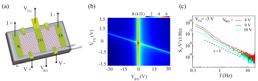
Our device is a stack of hBN/Graphene/hBN. It is prepared following the dry transfer technique[33]. First a thick hBN ( nm) is exfoliated on \ceSi/SiO2 substrate. A piece of glass slide is prepared with a layer of pmma and graphene is exfoliated on the pmma. The glass slide containing the graphene is then loaded on micro manipulator and the graphene flake is transferred on the hBN. The prepared stack of hBN/Graphene on \ceSi/SiO2 is then cleaned in acetone followed by IPA cleaning. Standard lithography technique is used to design the contacts which is followed by thermal evaporation of Cr (5 nm)/Au (70 nm) at a base pressure of 3e-7 mbar. The prepared device is then vacuum annealed at 300 ∘C for 3 hours. This is followed by transfer of a thin hBN ( nm) on prepared stack of hBN/Graphene. This thin top hBN act as a dielectric and top gate is defined using another lithography step followed by thermal evaporation of Cr (5 nm)/Au (70 nm).
Figure 1(a) shows the device schematic. The degenerately doped silicon (Si) acts as a global back gate () with 285 nm thick silicon dioxide (\ceSiO2) as the dielectric. The global back gate controls the carrier density throughout the graphene channel while the local top gate () tunes the density on a very small region of graphene (Fig. 1(a)). The length and width of graphene channel is 8 and 2 , respectively. The distance between voltage probe is 4 and top gate width is 1 . Figure 1(b) shows the 2D color plot of four probe resistance as a function of and . The diagonal and vertical lines represents the Dirac point under the top gate and back gate region, respectively. From slope of the diagonal line, we calculate the top hBN thickness 11 nm. All the measurements are performed in liquid Nitrogen at 77 K.
The noise is generally characterized using Hooge’s emperical relation:
| (1) |
where is the normalized current noise density, is the frequency, is the current, is the total number of charge carriers and is the Hooge parameter. The exponent is ideally expected to be 1 for noise. The noise measurement is performed following the measurement scheme discussed in our previous work[31, 34].
The noise measurements were performed at a constant current bias of 200 nA.
Figure 1(c) shows the normalized current noise density () at for three representative . We see clear behaviour. The black dash line shows the pure noise behaviour with . For our measurement we find in between 0.9 to 1.1 at various carrier concentration, suggesting that the charge traps are distributed randomly.[35, 29]
The noise amplitude (A) is defined as:[36]
| (2) |
Here and are the noise spectral density and source-drain current at m different frequencies . This method of defining noise amplitude helps to reduce the measurement error which comes by measuring noise amplitude at particular frequency[18, 24].
Figure 2 (a)-(c), plots the noise amplitude as a function of at -3 V, 0 V and 3 V, respectively. The corresponding four probe resistance is presented in the bottom panel (Fig. 2 (d)-(f)). The resistance peak close to (Fig. 2(e)) and (Fig. 2 (d-f)) corresponds to the Dirac point in the top gate and back gate region, respectively. We find that the over all noise amplitude value is smaller compared to graphene on \ceSi/SiO2 substrate. This is consistent with the previous reports[29, 30, 31, 32] . More interestingly, we find a strong noise amplitude peak far away from the Dirac point, in the electron doped region at V meV , although the resistance curves do not show any special feature around this density. We also find that this noise peak is independent of the top gate voltages. On the contrary, for the hole doped region ( in Fig. 2 (a)-(c) and in Fig. 2(b)) the noise is independent of carrier density. The noise behaviour close to Dirac point is very intricate and we shall discuss it in coming section.
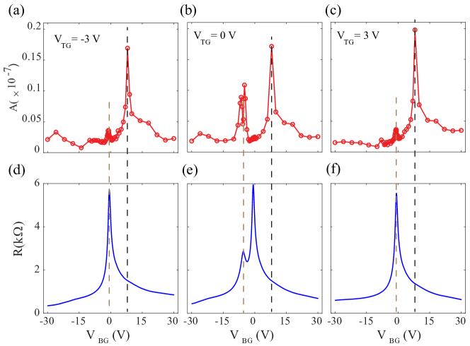
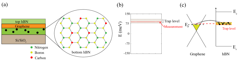
In this section, we explore the origin of noise peak at 8 V ( 6.4 and 90 meV). Recent study of Onodera et al.[15, 17] in graphene on Carbon doped hBN substrate show that carbon rich domain can exist even after mechanical exfoliation process and it affects the magneto-resistance drastically. Since the doped hBN flakes can’t be differentiated from the pristine hBN flakes in an optical microscope, photo luminance technique was used to identify the hBN flakes with carbon doped region and the pristine region. The graphene devices on pristine hBN and carbon doped hBN resulted in devices with ultra-high mobility and poor mobility, respectively. Furthermore, using magneto-resistance study, the energy of Carbon impurity level was estimated around meV. The DFT calculation in AB-stacked hBN-graphene heterostructure showed the presence of addition impurity states at 150 meV and 1.35 eV above the Dirac point for the Nitrogen and Boron site being doped by Carbon in hBN crystal, establishing that the magneto-resistance anomaly observed in graphene is due to Carbon doping at Nitrogen sites in hBN crystal (Fig. 3(a))[17].We plot in Fig 3(b) the impurity states measured by Onodera et al. [17], due to Carbon doping at Nitrogen site in the hBN crystal. We find that the Fermi energy of the observed noise peak ( 90 meV) in Fig. 2 (a)-(c) lies in the impurity energy range (80-110 meV), obtained by Onodera et al. [17], indicating that the noise peak in the electron doped regime is associated with the acceptor like impurity states formed due to Carbon doping at Nitrogen sites in hBN crystal. Schematic of the Carbon defects in the hBN layer is shown in Fig. 3(a). Defects states are distributed randomly at different heights from the adjacent graphene layer. The Carbon atom substituted at the Nitrogen sites in hBN layer is presented in Fig. 3(a) zoom in.
The physical mechanism of noise in graphene has been explained using the Hooge’s mobility fluctuation[37, 38, 39, 40, 41] or McWhorter charge number fluctuation method[42, 43] or both. Furthermore, both these mechanisms are correlated [29, 39]. Assuming that hBN is free of trap states or dangling bonds, the low noise amplitude in graphene on hBN substrate were explained by screening of charge carriers in graphene from the trap states in \ceSi/SiO2 by the hBN layer [29, 30].
Here we consider the effect of Carbon doped hBN on noise amplitude in the adjacent graphene layer. As discussed earlier, doping of Carbon atom at the Nitrogen sites in hBN crystal creates an impurity states meV above the Dirac point in the hBN (Fig. 3(b)). These defect states can act as a strong scattering center leading to trapping / de-trapping of charge carrier in graphene implying charge number fluctuation in the graphene layer. The trapping/ de-trapping events (Fig. 3(c)) will be maximum when the Fermi level in graphene layer matches with the defect energy level in hBN, leading to large noise peak. As we move away from the defect energy level, the trapping/de-trapping events will reduce leading to decrease in noise amplitude. Our work is in very good agreement with the recent theoretical work by Francesco [44], where they predicted noise peak in the conduction band of graphene, assuming McWhorter charge number fluctuation model. The noise peak was associated to the trap energy centred far away form the Dirac point in the conduction band.
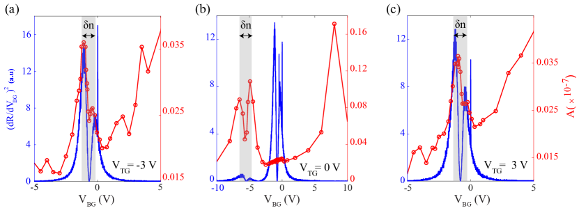
We now focus on the noise behaviour close to Dirac point. Figure 4 shows the noise amplitude (right Y axis) and (left Y axis) as a function of back gate voltage at three different top gate voltages around the Dirac point. The dip and peaks in corresponds to the Dirac point and the charge inhomogeneity () of the device. We observe clean “M-shape” noise behaviour near the Dirac point in the top gate region (Fig. 4b). Furthermore, the noise amplitude peaks and dip coincide with peak and dips, suggesting that noise is minimum exactly at the Dirac point. Noise value increases in between the Dirac point and , with the noise peak at . With the further increase in carrier density (), noise decreases and becomes almost flat beyond , for the hole doped region. Fig. 4a and Fig. 4c shows noise behaviour resembling "M-shape" with one peak having larger magnitude than the other peak and not so prominent dip at the Dirac point. This is referred as "asymmetric M-shape" noise, which may arise due to the intricate and convoluted way in which Fermi energy and trap energy vary over the device area[26]. We also observe smaller noise amplitude in the back gate region, without "M-shape" (Fig. 4b). This may be related to the gate area size. Since back gate and top gate has different area we can compare the area normalized noise amplitude, where A, L and W are the noise amplitude, length and width of the top gated or back gated region. We find very similar area normalized noise amplitude in top (), and back gate () region with and . The smearing of "M-shape" noise due to spatial variation of Fermi energy or charge inhomogeneity can lead to the disappearance of "M-shape" noise behaviour[26].
The charge inhomogeneity model of Xu et al.[18], which has been used in past to explain noise in graphene on \ceSi/SiO2 substrate can qualitatively explain the “M-shape” noise behaviour near Dirac point in our device. According to Hooge’s relation, noise at Dirac point can be written as . Here factor of 2 is because both electron and hole puddle contribute to the noise, , and D corresponds to the charge inhomogeneity and the electron-hole puddle size, respectively. Between the Dirac point and charge inhomogeneity point the noise amplitude can be written as . The application of positive gate voltage will increase electron density. Moreover, it will also increase electron puddle size and decrease the hole puddle size. Thus, in this region the noise contribution due to hole (minority carrier) is greater than the electrons (majority carrier) and hence noise increases. Beyond the spatial charge inhomogeneity region, the minority carrier puddle region (holes) starts shrinking and can no longer contribute to the conduction. Hence the majority carriers (i.e electrons) starts contributing to the noise and total noise is given by , implying decrease in noise value with increasing carrier density. Thus, the noise at the Dirac point is minimum, between the Dirac point and charge inhomogeneity point noise increases and is dominated by the minority charge carriers and beyond charge inhomogeneity point noise decreases and is governed by majority charge carriers. At higher hole density () noise becomes independent of gate voltage, which is consistent with the literature[29, 30].
In conclusion, we show that noise is an extremely sensitive tool to probe the defects states in the hBN substrate. The defects states arising due to Carbon doping at the Nitrogen sites in hBN crystal manifests itself as noise peaks in the adjacent graphene layer, although no signature is visible in the transport measurement. Furthermore, we show that noise near the Dirac point is dominated by inhomogeneous charge distribution of the device. We believe, our study will establish noise as a effortless technique to distinguish Carbon rich hBN from pure hBN crystal.
Authors thank Francesco M. D. Pellegrino for enlightening discussions.
DATA AVAILABILITY
The data that support the findings of this work are available from
the corresponding authors upon reasonable request.
REFERENCES
References
- Gorbachev et al. [2012] R. Gorbachev, A. Geim, M. Katsnelson, K. Novoselov, T. Tudorovskiy, I. Grigorieva, A. MacDonald, S. Morozov, K. Watanabe, T. Taniguchi, et al., Nature Physics 8, 896 (2012).
- Taychatanapat et al. [2013] T. Taychatanapat, K. Watanabe, T. Taniguchi, and P. Jarillo-Herrero, Nature Physics 9, 225 (2013).
- Bolotin et al. [2009] K. I. Bolotin, F. Ghahari, M. D. Shulman, H. L. Stormer, and P. Kim, Nature 462, 196 (2009).
- Young et al. [2012] A. F. Young, C. R. Dean, L. Wang, H. Ren, P. Cadden-Zimansky, K. Watanabe, T. Taniguchi, J. Hone, K. L. Shepard, and P. Kim, Nature Physics 8, 550 (2012).
- Amet et al. [2014] F. Amet, J. Williams, K. Watanabe, T. Taniguchi, and D. Goldhaber-Gordon, Physical review letters 112, 196601 (2014).
- Kumar et al. [2018a] C. Kumar, S. K. Srivastav, and A. Das, Physical Review B 98, 155421 (2018a).
- Yankowitz et al. [2012] M. Yankowitz, J. Xue, D. Cormode, J. D. Sanchez-Yamagishi, K. Watanabe, T. Taniguchi, P. Jarillo-Herrero, P. Jacquod, and B. J. LeRoy, Nature physics 8, 382 (2012).
- Ponomarenko et al. [2013] L. Ponomarenko, R. Gorbachev, G. Yu, D. Elias, R. Jalil, A. Patel, A. Mishchenko, A. Mayorov, C. Woods, J. Wallbank, et al., Nature 497, 594 (2013).
- Dean et al. [2013] C. R. Dean, L. Wang, P. Maher, C. Forsythe, F. Ghahari, Y. Gao, J. Katoch, M. Ishigami, P. Moon, M. Koshino, et al., Nature 497, 598 (2013).
- Barrier et al. [2020] J. Barrier, P. Kumaravadivel, R. K. Kumar, L. Ponomarenko, N. Xin, M. Holwill, C. Mullan, M. Kim, R. Gorbachev, M. Thompson, et al., Nature communications 11, 1 (2020).
- Huang et al. [2017] B. Huang, G. Clark, E. Navarro-Moratalla, D. R. Klein, R. Cheng, K. L. Seyler, D. Zhong, E. Schmidgall, M. A. McGuire, D. H. Cobden, et al., Nature 546, 270 (2017).
- Khestanova et al. [2018] E. Khestanova, J. Birkbeck, M. Zhu, Y. Cao, G. Yu, D. Ghazaryan, J. Yin, H. Berger, L. Forro, T. Taniguchi, et al., Nano letters 18, 2623 (2018).
- Cao et al. [2015] Y. Cao, A. Mishchenko, G. Yu, E. Khestanova, A. Rooney, E. Prestat, A. Kretinin, P. Blake, M. B. Shalom, C. Woods, et al., Nano letters 15, 4914 (2015).
- Jin et al. [2019] C. Jin, E. C. Regan, A. Yan, M. I. B. Utama, D. Wang, S. Zhao, Y. Qin, S. Yang, Z. Zheng, S. Shi, et al., Nature 567, 76 (2019).
- Onodera et al. [2019] M. Onodera, K. Watanabe, M. Isayama, M. Arai, S. Masubuchi, R. Moriya, T. Taniguchi, and T. Machida, Nano letters 19, 7282 (2019).
- Watanabe and Taniguchi [2019] K. Watanabe and T. Taniguchi, npj 2D Materials and Applications 3, 1 (2019).
- Onodera et al. [2020] M. Onodera, M. Isayama, T. Taniguchi, K. Watanabe, S. Masubuchi, R. Moriya, T. Haga, Y. Fujimoto, S. Saito, and T. Machida, Carbon 167, 785 (2020).
- Xu et al. [2010] G. Xu, C. M. Torres Jr, Y. Zhang, F. Liu, E. B. Song, M. Wang, Y. Zhou, C. Zeng, and K. L. Wang, Nano letters 10, 3312 (2010).
- Rumyantsev et al. [2010] S. Rumyantsev, G. Liu, W. Stillman, M. Shur, and A. Balandin, Journal of Physics: Condensed Matter 22, 395302 (2010).
- Heller et al. [2010] I. Heller, S. Chatoor, J. Mannik, M. A. Zevenbergen, J. B. Oostinga, A. F. Morpurgo, C. Dekker, and S. G. Lemay, Nano letters 10, 1563 (2010).
- Zhang et al. [2011] Y. Zhang, E. E. Mendez, and X. Du, ACS nano 5, 8124 (2011).
- Pal et al. [2011] A. N. Pal, S. Ghatak, V. Kochat, E. Sneha, A. Sampathkumar, S. Raghavan, and A. Ghosh, ACS nano 5, 2075 (2011).
- Kaverzin et al. [2012] A. Kaverzin, A. S. Mayorov, A. Shytov, and D. Horsell, Physical Review B 85, 075435 (2012).
- Lin and Avouris [2008] Y.-M. Lin and P. Avouris, arXiv preprint arXiv:0801.4576 (2008).
- Pal and Ghosh [2009] A. N. Pal and A. Ghosh, Applied Physics Letters 95, 082105 (2009).
- Pellegrini [2013] B. Pellegrini, The European Physical Journal B 86, 1 (2013).
- Shao et al. [2009] Q. Shao, G. Liu, D. Teweldebrhan, A. A. Balandin, S. Rumyantsev, M. S. Shur, and D. Yan, IEEE Electron Device Letters 30, 288 (2009).
- Karnatak et al. [2016] P. Karnatak, T. P. Sai, S. Goswami, S. Ghatak, S. Kaushal, and A. Ghosh, Nature communications 7, 13703 (2016).
- Stolyarov et al. [2015] M. A. Stolyarov, G. Liu, S. L. Rumyantsev, M. Shur, and A. A. Balandin, Applied Physics Letters 107, 023106 (2015).
- Kayyalha and Chen [2015] M. Kayyalha and Y. P. Chen, Applied Physics Letters 107, 113101 (2015).
- Kumar et al. [2016] C. Kumar, M. Kuiri, J. Jung, T. Das, and A. Das, Nano letters 16, 1042 (2016).
- Kakkar et al. [2020] S. Kakkar, P. Karnatak, M. A. Aamir, K. Watanabe, T. Taniguchi, and A. Ghosh, Nanoscale 12, 17762 (2020).
- Zomer et al. [2011] P. Zomer, S. Dash, N. Tombros, and B. Van Wees, Applied Physics Letters 99, 232104 (2011).
- Kumar et al. [2018b] C. Kumar, M. Kuiri, and A. Das, Solid State Communications 270, 38 (2018b).
- Balandin [2002] A. A. Balandin, Noise and fluctuations control in electronic devices (Amer. sci. publ. Stevenson Ranch (Ca), 2002).
- Balandin [2013] A. A. Balandin, Nature nanotechnology 8, 549 (2013).
- Zahid Hossain et al. [2013] M. Zahid Hossain, S. Rumyantsev, M. S. Shur, and A. A. Balandin, Applied Physics Letters 102, 153512 (2013).
- Rumyantsev et al. [2013] S. Rumyantsev, D. Coquillat, R. Ribeiro, M. Goiran, W. Knap, M. Shur, A. Balandin, and M. Levinshtein, Applied Physics Letters 103, 173114 (2013).
- Vail et al. [2020] O. Vail, J. Hankinson, C. Berger, W. de Heer, and Z. Jiang, Applied Physics Letters 117, 083105 (2020).
- Cultrera et al. [2018] A. Cultrera, L. Callegaro, M. Marzano, M. Ortolano, and G. Amato, Applied Physics Letters 112, 093504 (2018).
- Takeshita et al. [2016] S. Takeshita, S. Matsuo, T. Tanaka, S. Nakaharai, K. Tsukagoshi, T. Moriyama, T. Ono, T. Arakawa, and K. Kobayashi, Applied Physics Letters 108, 103106 (2016).
- Peng et al. [2017] S. Peng, Z. Jin, D. Zhang, J. Shi, D. Mao, S. Wang, and G. Yu, ACS applied materials & interfaces 9, 6661 (2017).
- Wang et al. [2021] Y. Wang, V. X. Ho, Z. N. Henschel, M. P. Cooney, and N. Q. Vinh, ACS Applied Nano Materials 4, 3647 (2021).
- Pellegrino et al. [2020] F. M. Pellegrino, G. Falci, and E. Paladino, Communications Physics 3, 1 (2020).