Probing the electromagnetic response of dielectric antennas by vortex electron beams
Abstract
Focused beams of electrons, which act as both sources, and sensors of electric fields, can be used to characterise the electric response of complex photonic systems by locally probing the induced optical near fields. This functionality can be complemented by embracing the recently developed vortex electron beams (VEBs), made up of electrons with orbital angular momentum, which could, in addition, probe induced magnetic near fields. In this work, we revisit the theoretical description of this technique, dubbed vortex Electron Energy-Loss Spectroscopy (v-EELS). We map the fundamental, quantum-mechanical picture of the scattering of the VEB electrons to the intuitive classical models, which treat the electron beams as a superposition of linear electric and magnetic currents. We then apply this formalism to characterise the optical response of dielectric nanoantennas with v-EELS. Our calculations reveal that VEB electrons probe electric or magnetic modes with different efficiency, which can be adjusted by changing either beam vorticity or acceleration voltage to determine the nature of the probed excitations. We also study a chirally-arranged nanostructure, which in the interaction with electron vortices produces dichroism in electron energy loss spectra. Our theoretical work establishes VEBs as versatile probes that could provide information on optical excitations otherwise inaccessible with conventional electron beams.
I Introduction
Electron energy-loss spectroscopy (EELS) in a scanning transmission electron microscope (STEM) Egerton (2011) is an emerging technique to characterize optical excitations with high spatial and spectral resolution García de Abajo (2010); Nelayah et al. (2007); Lagos et al. (2017); Govyadinov et al. (2017). Recent experimental and theoretical studies have demonstrated the capabilities of STEM-EELS to map near fields of localized surface polaritons in plasmonic and phononic nanostructures that are of high interest in the field of nanophotonics for their applications in focusing and engineering light below the diffraction limit Giannini et al. (2011); Pelton et al. (2008).
An alternative possibility to control light at the nanoscale is to use resonant electromagnetic (EM) modes in nanoparticles made of materials with high refractive index Kuznetsov et al. (2016); Jahani and Jacob (2016); Verre et al. (2019); Evlyukhin et al. (2012); Albella et al. (2014); Cambiasso et al. (2017), which have been, however, relatively rarely studied by near-field spectroscopic methods Bakker et al. (2015); Habteyes et al. (2014); Miroshnichenko et al. (2015); Frolov et al. (2017); Coenen et al. (2013); van de Groep et al. (2016). It has been shown only by recent experiments that focused electron beams such as those used in STEM-EELS can probe the response of dielectric antennas Liu et al. (2019); Kfir et al. (2020); Alexander et al. (2021). Here we explore the possibilities of using focused electron probes to distinguish electric and magnetic modes and hot spots that are crucial for applications of dielectric particles in nanophotonics Cihan et al. (2018); Regmi et al. (2016); Rutckaia et al. (2017); Schmidt et al. (2012); Vaskin et al. (2019), and thus fully characterize the properties of their resonant modes.
Interestingly, besides conventional electron beams, recent efforts have led to the generation of vortex electron beams (VEBs) in (S)TEM Bliokh et al. (2007); Lloyd et al. (2017); Bliokh et al. (2017); Uchida and Tonomura (2010); McMorran et al. (2011); Béché et al. (2014); Mafakheri et al. (2017); Vanacore et al. (2019); Tavabi et al. (2020). VEBs carry orbital angular momentum (OAM), which could facilitate direct interaction of the beam with excitations of both electric and magnetic nature. Besides various applications in probing magnetic fields Guzzinati et al. (2013); Grillo et al. (2017), magnetic transitions in bulk materials Verbeeck et al. (2010); Lloyd et al. (2012); Yuan et al. (2013); Rusz et al. (2016) and chirality of crystals Juchtmans et al. (2015), the introduction of VEBs (and other shaped beams) in electron microscopy by using adjustable phase plates Verbeeck et al. (2018); Konečná and García de Abajo (2020); García de Abajo and Konečná (2021) might also open a pathway for symmetry-based selective excitation of EM modes in photonic nanostructures Ugarte and Ducati (2016); Guzzinati et al. (2017); Zanfrognini et al. (2019), separation of electric and magnetic modes Mohammadi et al. (2012), or for developing the local investigation of the dichroic response of chiral nanoantennas Asenjo-Garcia and García de Abajo (2014); Zanfrognini et al. (2019).
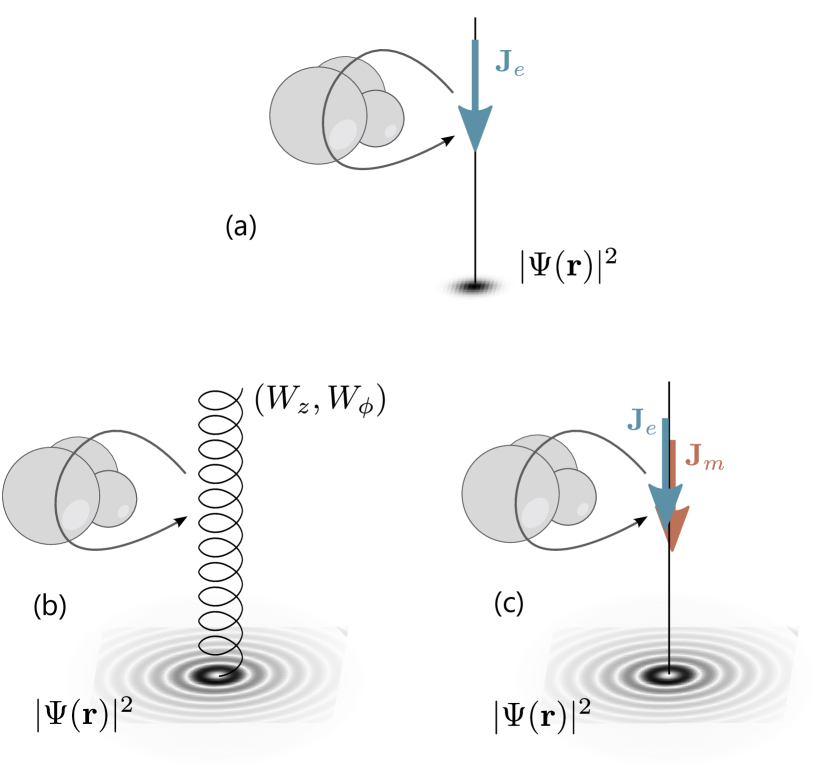
In this work, we show that STEM-EELS with the use of either a conventional or a vortex beam might be a suitable technique for distinguishing between the electric and magnetic nature of electromagnetic modes supported by dielectric antennas. We start by introducing a quantum-mechanical description of the inelastic interaction of VEBs with a general (classically responding) sample and with a point-like polarizable object, for which we obtain a closed form in the limit of a tightly focused VEB. To introduce the possibility of calculating the EEL spectrum with a VEB (v-EELS) for a spatially extended nanostructure, we find a source equivalent to the VEB within the framework of classical electrodynamics (see Fig. 1) and perform fully retarded calculations to retrieve the electromagnetic field arising from the VEB-sample interaction. We calculate EEL spectra considering the interaction with electron beams of both zero and non-zero OAM. We study single and dimer dielectric antennas of different shapes, particularly spherical and cylindrical structures made of silicon. We show that by varying excitation parameters or by comparing the spectra acquired with a non-vortex and a vortex beam, fast electrons preferentially couple to modes of electric and magnetic nature, respectively. Finally, we explore dichroism in v-EELS emerging for a chiral dielectric nanostructure.
II Theoretical framework for vortex electron energy loss spectroscopy at optical frequencies
II.1 Quantum-mechanical description of the beam
The wavefunction of a vortex electron , can be described in the non-relativistic approximation (for discussion of the relativistic solutions, see Refs. Bialynicki-Birula and Bialynicka-Birula (2017); Barnett (2017)) as a solution of the Schrödinger equation for a free-space moving electron with a non-vanishing OAM . In cylindrical coordinates , one of the simplest solutions takes the form of a Bessel beam Bliokh et al. (2007); Lloyd et al. (2017); Bliokh et al. (2017)
| (1) |
where and are the radial and perpendicular wavevector components of the electron with mass moving along the axis at velocity , respectively, stands for a normalization area and for a normalization length, is the reduced Planck constant. The Bessel function of order , , governs the radial shape variation of the beam profile, whereas the helical form of the wavefront is captured through the exponential term .
We now express the probability of losing energy per electron considering a transition from a well-defined initial state to final states (following the formalism introduced in Ref. Asenjo-Garcia and García de Abajo (2014)), due to the interaction with the structured environment, as
| (2) |
where is the elementary charge, is the final/initial electron energy, is the Green’s tensor describing the electromagnetic response of the probed structure and where we sum over the final states.
In the following, we restrict ourselves to the states and with initial and final longitudinal wavevector components and , respectively. We further consider with a set of possible transverse wavevectors and a well-defined initial transverse wavefunction component where is an initial wavevector cutoff. The centers of the forming and collection apertures are assumed to be aligned on top of each other.
Considering a detector imposing a cutoff of transverse final wavevectors due to a finite collection angle, we can replace the schematic sum over final states with . We also rewrite the spatial integrals over and in cylindrical coordinates, and collect all the - and -dependent exponentials from the ’s [see Eq. (1)] to evaluate the integral in the non-recoil approximation
| (3) |
Defining
| (4) |
we can express the loss probability as
| (5) |
Above we introduced , , and defined the vector field related to the gradient of electron’s wavefunctions
| (6) |
where denote unit vectors along the directions .
When all electrons are collected by the detector (), we can use the identity to perform the integral over the final transverse wavevectors to get
| (7) |
Note that will be strongly peaked around an effective initial VEB radius given by the initial cutoff value. Therefore if we consider slowly varying around , we can roughly approximate the integral over by to obtain
| (8) |
where we disregarded the radial component of as it is much smaller than the other components around , yielding
| (9) |
This formulation of v-EELS is depicted schematically in Fig. 2(a).
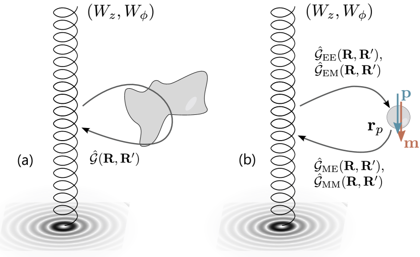
II.2 Loss probability for a VEB interacting with a point-like dipolar particle in a focused beam limit
The formulation of the loss probability given in Eq. (8) is general, but does not easily simplify to a classical picture, widely embraced to address conventional EELS. To aid that simplification, here we present a calculation of loss probability due to the interaction with a specific system — a point-like dipolar particle shown in Fig. 2(b). We will use this result in the following Section II.3 to identify a semi-classical description, shown schematically in Fig. 1(c).
The point-like scatterer is situated at , and is electrically and magnetically polarizable in the direction, and characterized by the electric polarizability tensor , magnetic polarizability tensor , and crossed electric-magnetic and magnetic-electric polarizability tensors and , respectively. The latter two tensors are responsible for a dichroic response and fulfill . For simplicity, we assume the response only in the direction, however, a general direction should be considered in a realistic scenario. The Green’s tensor is then
| (10) |
with and , where with the speed of light , is the vacuum permittivity and denotes tensor product.
The integrals over (and ) involved in [see Eq. (4)] are analytical Asenjo-Garcia and García de Abajo (2014):
| (11) |
and
| (12) |
which we use to obtain
where all tensors also depend on . We can expand the products of the currents and Green’s functions in the rhs of Eq. (8) as
| (13) |
The first term expands as
| (14) |
where the three terms vanish due to the symmetries of the Green’s functions (e.g. ), and the axial form of the polarizability. Similarly, one we can simplify
| (15) |
| (16) |
| (17) |
We now split the total loss probability as
| (18) |
where the individual contributions are defined by the products of the components of , i.e. , , , :
| (19) |
where we assumed , and introduced the Lorentz factor . With the same assumptions, we obtain:
| (20) |
and
| (21) |
We evaluated the integrals following Ref. Asenjo-Garcia and García de Abajo (2014). We note that for a well-focused VEB with , , and thus using and for small arguments, we obtain
| (22) |
The well-focused-VEB limit is very accurate for nm at optical frequencies and for typical TEM acceleration voltages. Such effective radii are achievable even for relatively large () as shown in Appendix A. We also note that for , the result above coincides with the classical limit with a well-focused beam at the origin interacting with an electric dipole oriented along the axis.
The loss probability in Eq. (22) can be readily evaluated for a beam carrying OAM and , which yields the dichroic signal
| (23) |
where we used . Interestingly, the proportionality of the dichroic signal to holds also for the difference of optical absorption obtained with right- and left-handed circularly polarized light () Tang and Cohen (2010). However, compared to the optical circular dichroism, the local excitation by a focused VEB makes it possible to probe the dichroic response with high spatial resolution, which is manifested in the fast decay of the signal strength with increasing distance of the electron beam from the particle, as the EEL probability strongly depends on the field accompanying the VEBs.
Importantly, considering typical scaling of polarizability components ( and ), we can see that the contribution to the loss probability due to the interaction with the electric dipole will be dominant as at optical frequencies and typical velocities of electron probes. Significant improvements in detecting dichroism or purely magnetic response from point-like objects with well-focused VEBs could be achieved by employing slower electrons with large OAM.
II.3 Semi-classical formalism
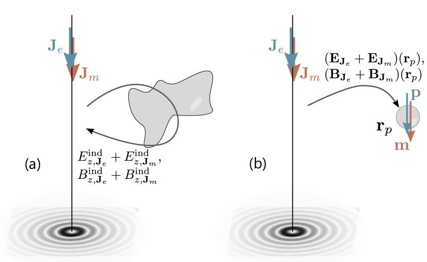
The interaction of a well-focused VEB with a sample can also be expressed using a semi-classical formalism by introducing effective frequency-dependent electric and magnetic line currents and , respectively, representing the VEB. These sources induce the electromagnetic response of a sample, which acts back on the electron beam and causes its energy loss García de Abajo (2010) [see schematic in Fig. 3(a)]. While we expect that the electric current of a VEB will have a simple form, identical to that used throughout the literature on conventional EELS García de Abajo (2010), we seek to identify the exact expression for the magnetic current.
The total energy loss consists of the energy loss experienced by both the electric and the magnetic current components of the beam: . The electric and the magnetic energy losses in the non-recoil approximation are given by Mohammadi et al. (2012)
| (24) |
| (25) |
where and are electric and the magnetic fields, respectively, induced by the radiation from the electric and magnetic currents and , respectively. The last two expressions can be related using the invariance of the Maxwell’s equations, and the corresponding Green’s functions, in free space, under the transformation Novotny and Hecht (2006)
| (26) |
We can now introduce the electric and magnetic loss probabilities and , respectively, as . The total loss probability
| (27) |
then corresponds to the measured electron energy loss spectrum for the case that a perfectly focused VEB is employed and that we disregard OAM exchange.
We find that the line current density sources mimicking the well-focused excitation by a VEB centered at are expressed as
| (28) |
where is the amplitude of the electric current density and is a (complex) amplitude of the effective magnetic current density to be determined. By inserting the current densities from Eq. (28) into Eqs. (24) and (25), we can write down an analogue of Eq. (18), expressing the total loss probability of the sum of the four contributions
| (29) |
where
| (30) |
| (31) |
Here we split the induced electric field excited by the electric and the magnetic current ( and ), yielding the corresponding loss probabilities and , respectively. Similarly, the induced magnetic field originates from the interaction of the sample with both current sources ( and ), giving rise to the loss channels and . This is denoted schematically in Fig. 3(a).
Loss probability for a VEB interacting with a point-like dipolar particle in a semi-classical model
To identify the correct expression for the magnetic current amplitude, we now aim to find the correspondence between the total loss given in Eq. (29), and the result considering the quantum-mechanical description of the VEB given in Eq. (8). To this end, we consider here the same problem of scattering on a point-like dipolar particle as discussed in Section II.2.
The calculations are carried out in a different manner than above, shown schematically in Fig. 3(b). Here we consider the electric and magnetic dipolar moments, and respectively, induced in the scatterer and , by the fields generated by the electric and magnetic currents of the VEB:
| (32) |
| (33) |
where
| (34a) | |||
| (34b) | |||
and
| (35a) | |||
| (35b) | |||
The loss of energy can be then calculated by considering the work done in the scatterers as:
| (36) |
Plugging in Eqs. (34) and (35) into the above expression, and axial polarizabilities as considered in Sec. II.2, we can find a closed expression for the loss probability:
| (37) |
If we compare Eq. (37) with Eq. (22), we find
| (38) |
where we introduced Bohr magneton, and set as we are anyways disregarding the OAM exchange during the interaction.
In connection with our definition of different contributions to the loss probability, we can now see that the dichroic contribution stems from the crossed interaction between the electrically induced magnetic response and the magnetic current and vice versa, contained in the terms and , respectively.
III Loss probability for VEBs interacting with dielectric particles in the semi-classical approximation
In the following, we present calculations of the loss probabilities [Eqs. (30) and (31)] for different sample geometries where we solve for the induced EM field either analytically or numerically (as described in Appendix C).
III.1 Spectroscopy of localized modes in spherical dielectric nanoantennas
We first apply the theory presented above to the canonical example of a single spherical nanoparticle. Due to its symmetry, the terms and do not contribute to the loss probability and we need to evaluate only the terms and . The fully-retarded analytical solution of the induced electric field arising from the excitation of a spherical particle by an electric current was obtained in Ref. García de Abajo (1999), and the corresponding EEL probability is expressed as:
| (39) |
where the summation is performed over multipoles , is the modified Bessel function of the second kind of order , is the distance of the beam from the center of the sphere (the impact parameter), and the coefficients take into account the coupling with the field of the electron beam (see Eqs. (30) and (31) of Ref. García de Abajo (1999)). We use superscripts M/E to denote the coefficients related to the excitation of the magnetic/electric modes. Eq. (39) also includes the Mie coefficients:
| (40) | ||||
| (41) |
where the wave vector inside the sphere characterized by the relative dielectric function , and is the radius of the sphere. and are the spherical Bessel and Hankel functions of the first kind, respectively. The derivatives in Eq. (40) and Eq. (41) are performed with respect to the functions’ arguments.
When we consider the excitation of the sphere by a magnetic current, the corresponding loss probability can be readily obtained by utilizing the transformation given by Eq. (26). The magnetic-current-mediated loss probability is thus given by
| (42) |
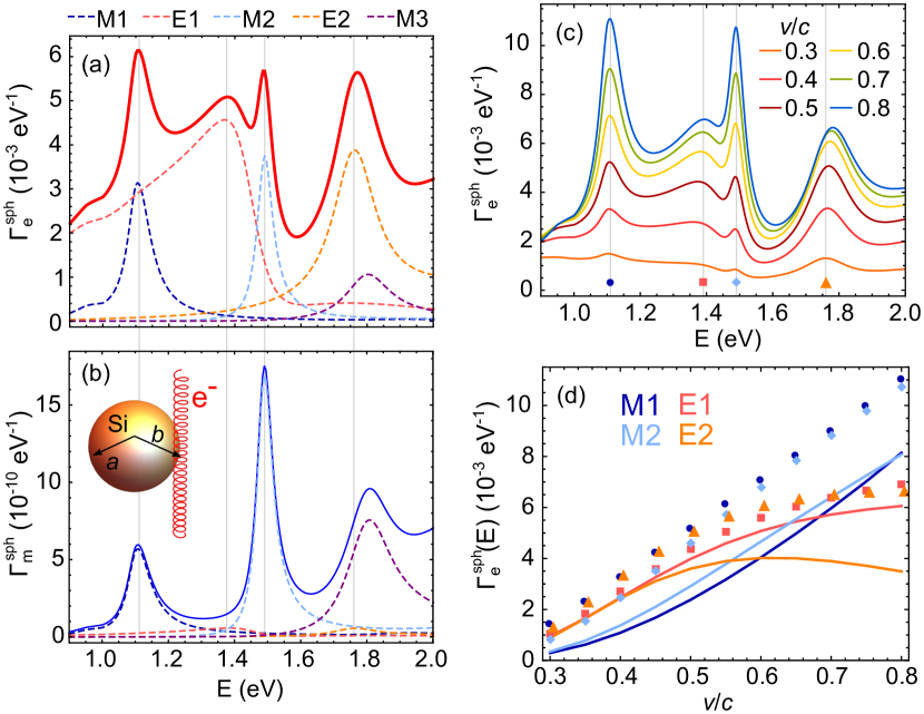
We now explore whether we can distinguish modes of electric and magnetic nature excited in silicon nanoparticles with the help of the v-EEL spectra. In Fig. 4(a,b) we show the calculated spectral contributions [Eq. (39); solid red line] and [Eq. (42); solid blue line], respectively, for a single silicon nanosphere with radius nm, an impact parameter nm [as depicted in the inset of Fig. 4(b)] and a 100 keV beam (). We note that while the spectrum in (a) does not depend on and thus is identical for a vortex and non-vortex beam, in (b) is nonzero only for a vortex beam. We considered for our vortex beam.
To understand the origin of the resulting spectral features, we split the full spectra (solid lines) into the contributions of the different electric (En) or magnetic (Mn) -order multipoles (dashed lines), i.e., the spectra in Eqs. (39) and (42) before the summation over . In the considered spectral range, the probability [solid red line in Fig. 4(a)] exhibits four well-distinguishable peaks, which arise due to the excitation of a magnetic dipolar mode (M1, dark blue dashed line), electric dipole (E1, light red dashed line), magnetic quadrupole (M2, light blue dashed line) and electric quadrupole (E2, orange dashed line), whose energy nearly coincides with the magnetic octupole (M3, purple dashed line). On the other hand, due to the interchange of the coupling coefficients [compare Eq. (39) vs. Eq. (42)], only the magnetic modes (M1, M2 and M3) are found in the plot of [solid blue line in Fig. 4(b)]. The cross-coupling of the magnetic current to the electric modes is negligible and produces only a small contribution [see dashed light red and orange lines in Fig. 4(b) close to zero].
In a typical measurement of EELS, one obtains the total loss probability [sum of solid spectra in (a) and (b)]. Therefore, in order to separate the loss probability components and , two measurements would be needed: one with a beam where and another one with exactly the same experimental conditions with a non-vortex beam (). After subtracting these two spectra, one would obtain , which only shows the peaks corresponding to the magnetic modes. Unfortunately, we can observe that even for relatively large OAM, the magnetic part of the loss probability is six orders of magnitude smaller than , and thus falls below the limit of the currently achievable signal-to-noise ratio in STEM-EELS experiments.
Besides varying the OAM of the VEB, there is another degree of freedom, which might be used to assign the spectral peaks to the modes as either electric or magnetic: the electron’s speed , which governs the strength of the coupling coefficients related to the electromagnetic field of the fast electrons. In Fig. 4(c) we evaluate for varying and (conventional electron beam). We observe that the intensity ratio of the four visible peaks changes significantly. With increasing accelerating voltage (electron’s speed), the coupling of the beam with the magnetic modes is much more efficient, which results from the fact that the accompanying magnetic field is stronger for faster electrons. Further, the intensity corresponding to the excitation of the M1 and M2 modes grows faster than the peak assigned to the E1 mode, which starts to saturate for larger speeds (). This trend is confirmed in Fig. 4(d), where we plot the intensities of the peaks extracted from spectra in Fig. 4(c) at the energies corresponding to the M1 (dark blue points), E1 (light red squares), M2 (light blue diamonds), and E2 (orange triangles) modes, depending on the electron’s speed. We also plot the peak intensities as if the modes were excited independently by solid lines to eliminate the influence of the spectral overlap of the excited modes [see Fig. 4(a) showing that, e.g., E1 contributes significantly even at the energy of the M1 peak]. This trend is similar for higher-order modes, and we suggest that obtaining the EEL spectra at several acceleration voltages might serve for a relatively straightforward classification of the modes.
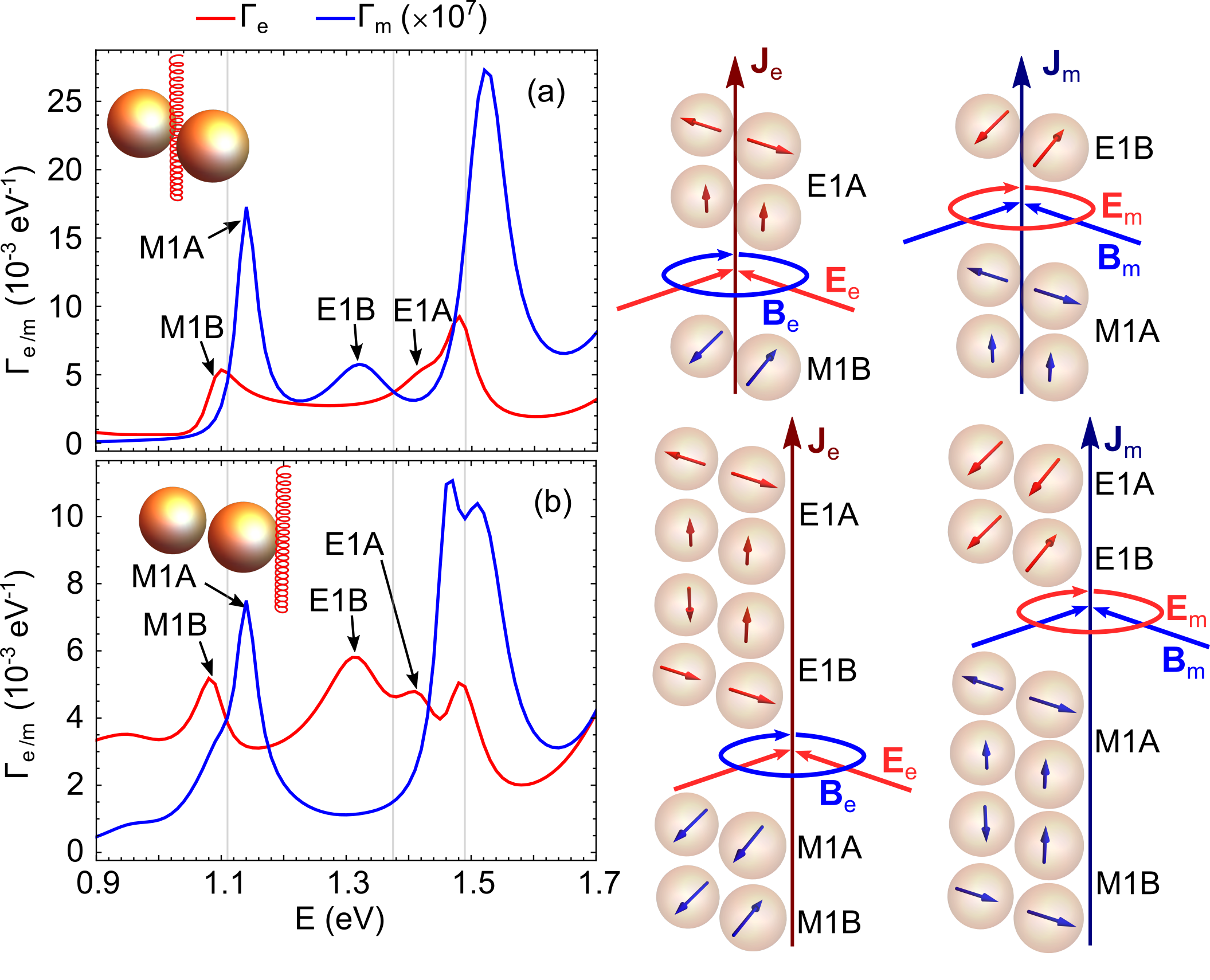
VEBs can also be applied to unravel the spectral response of more complex dielectric nanostructures, such as dimers of two (identical) particles separated by a small gap. The nanoparticle dimers are also of large interest as they can provide a significant enhancement of the field in the gap or yield directional scattering Fu et al. (2013); Albella et al. (2014); Bakker et al. (2015); Yan et al. (2015). In Fig. 5 we thus study numerically v-EELS of a pair of spherical dielectric particles (each of them with the same properties as the single spherical particle studied in Fig. 4) separated by a gap of distance nm. It has been shown that in such a system, the modes of the individual particles hybridize and form bonding and antibonding modes of the dimer Zywietz et al. (2015). In Fig. 5(a,b) we analyze how these hybridized modes contribute to the spectra for different VEB positions.
In Fig. 5(a,b) we consider a 100-keV electron beam with passing through the middle of the gap or close to the side of one of the spheres and calculate the EEL probability. We note that the crossed loss probability components and are either identically zero or cancel. We can thus again assign and . Importantly, the symmetry of the electric or magnetic field produced by the electric or magnetic part of VEB current dictates which current component couples to specific modes of the dimer. We schematically depict possible scenarios next to the graph.
If the electron beam is placed in the gap [Fig. 5(a)], [solid red line in Fig. 5(a)] shows that the electric current component can excite the magnetic dipolar bonding mode (M1B), the electric antibonding mode (E1A), and the bonding magnetic quadrupolar mode yielding a peak close to 1.5 eV. On the other hand, the magnetic part of the current couples to the magnetic dipolar anti-bonding mode (M1A), the electric dipolar bonding mode (E1B) and the anti-bonding magnetic quadrupolar mode (see the peak above 1.5 eV), which appears in [solid blue line in Fig. 5(a)]. The energy splitting of the bonding and anti-bonding modes is apparent when the peak positions are compared to the spectral positions of the modes excited in the individual sphere (plotted by vertical gray lines, extracted from Fig. 4).
When the beam is moved to the side of one of the spheres along the dimer axis [see the schematics in Fig. 5(b)], bonding and anti-bonding dipolar modes are excitable by both current components as schematically shown next to the graph. However, some of the dipolar arrangements are excited preferentially, which is apparent in the respective spectra. The electric component of the current efficiently couples with the M1B mode, E1A mode, and also E1B mode [solid red line in Fig. 5(b)]. On the other hand, [solid blue line in Fig. 5(b)] shows a spectral feature arising from the excitation of both M1A and M1B. Interestingly, M1A is dominant with respect to M1B, whose excitation gives rise to a small shoulder below 1.1 eV. We also observe that the magnetic current component couples only weakly to the E1B and E1A modes. However, we note that this loss contribution is still six to seven orders of magnitude smaller than the electric part and would be difficult to isolate, as discussed above.
III.2 Probing the photonic density of states in an infinite cylinder
Another canonical example of a dielectric system with a strong electric and magnetic response, which can be characterized via v-EELS, is that of dielectric waveguides Rybin et al. (2015); Holsteen et al. (2017); Cihan et al. (2018); Traviss et al. (2015); Abujetas et al. (2015); Cao et al. (2009). Previous theoretical analysis of the interaction of fast electrons with dielectric cylindrical waveguides has already suggested their potential for applications in single-photon sources Bendaña et al. (2011). Here we study the EEL probability of a VEB exciting an infinite cylindrical wire of radius placed in vacuum for a geometrical arrangement as sketched in Fig. 6: an electron beam moving at speed parallel to the axis of the wire at a distance from the center of the cylinder. For this geometry, the retarded analytical solution of the EEL probability was presented e.g. in Ref. Walsh (1991) and reproduced in Appendix D, which we can easily modify to include the contribution to the loss experienced by the magnetic component of the current by using the transformation in Eq. (26). We can write the two contributions to the overall loss probability of the VEB per unit length as:
| (43) | ||||
| (44) |
where denotes different azimuthal modes, is the Kronecker delta, and stands for the wavevector along the cylinder axis, which has to match the wavevector component transferred from the fast electron when calculating the spectra. The dimensionless coefficients and can be obtained as described in Appendix D. We also define .
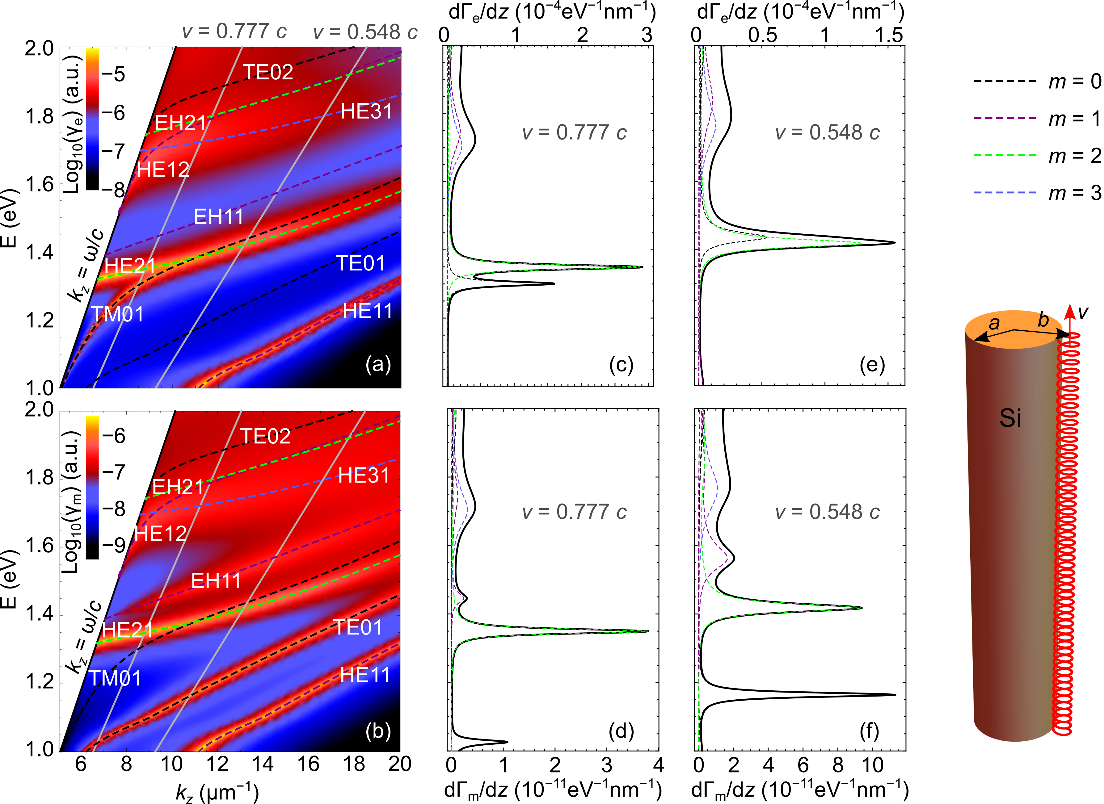
The denominators of the coefficients and yield the dispersion of all the modes supported by the cylinder with the relative dielectric function :
| (45) |
where and are the modified Bessel functions of the first and the second kind, respectively, of order , and .
In Fig. 6(a,b) we plot the -dependent loss probabilities and as implicitly defined in Eq. (43) and Eq. (44), respectively, for geometrical parameters nm and nm. On top of the density plots, we show the dispersion curves corresponding to the guided EM modes (the leaky modes above the light line, given by , are not shown as they are not excitable by the parallel beam) supported by the infinite cylinder obtained as solutions of Eq. (45) for the different orders denoting the modes’ azimuthal symmetry. We consider only the first four azimuthal numbers , and as higher-order modes are much more damped, with these modes we can capture all the dominant spectral features. We can observe that some of the modes (denoted by using the standard notation from waveguide theory, see e.g. Refs. Snitzer (1961); Tong et al. (2004)) are visible only in the electrical contribution to the spectra, [Fig. 6(a)] or, vice versa, in the magnetic contribution, [Fig. 6(b)]. We can conclude that due to the symmetry of the EM field produced by the current components, transverse electric modes (TE01, TE01,…) are excitable only by the magnetic current. On the contrary, transverse magnetic modes (TM01, TM02,…) couple only to the electric current component.
From the -dependent plots in Fig. 6(a,b) we can readily obtain the EEL spectra by setting [see the gray lines in Fig. 6(a,b)]. In Fig. 6(c,d) we plot [Eq. (43)] and [Eq. (44)], respectively, evaluated for a 300-keV electron beam (). The total probabilities (solid black lines) are split into contributions of the different azimuthal modes denoted by the colored dashed lines. We observe that the hybrid HE21 mode produces the dominant spectral feature in both cases. On the other hand, the peak corresponding to the excitation of the TM01 mode is present only in the spectrum of Fig. 6(c), and the peak arising from the excitation of the TE01 mode appears only in Fig. 6(d). The hybrid EH11 is also dominantly excitable by the magnetic current and has only a negligible contribution in the electric-current-mediated spectrum, as confirmed by evaluating the induced fields given in Appendix D.
By changing the acceleration voltage to 100 kV, we obtain the spectra in Fig. 6(e,f), where the same modes give rise to peaks at slightly different energies due to the change of the energy-momentum matching (higher is provided at fixed energy compared to the faster 300-keV electron). Importantly, the standard electrical component of the EEL probability in geometries possessing translational invariance, such as in the current situation of the beam moving parallel to an infinite cylinder, can be related to the electrical part of the projected photonic local density of states (LDOS)García de Abajo and Kociak (2008). An analogous proportionality holds between the magnetic-current-mediated loss and the magnetic part of the photonic LDOS. Hence, this relationship might be used in the context of the interaction of magnetic emitters with such structures. Our results are consistent with the findings in Ref. Verhart et al. (2014), where the coupling of modes to differently oriented electric dipoles was linked to the excitation by electric/magnetic current components.
III.3 Dichroic spectroscopy with vortex electron beams
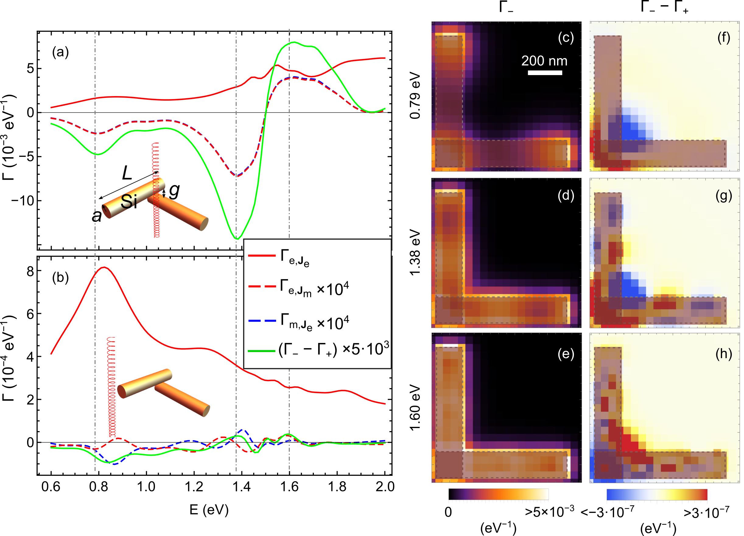
Now we demonstrate the emergence of the dichroic signal when an extended chirally-arranged nanostructure is probed by a VEB. We adopt a similar geometry as the one studied in Ref. Yin et al. (2013), and perform the numerical modeling for two vertically displaced cylindrical rods rotated by and stacked at their corners as shown in the schematics of Fig. 7. The overall response of the structure in such an arrangement yields optical dichroism Yin et al. (2013), and thus, according to the preceding analysis, we should expect the emergence of dichroism also in the v-EEL spectra. However, the finite spatial extent of the structure, as well as the overlap of different electro-magnetic modes excited in the silicon rods, might produce a non-trivial spatial dependence of the dichroic signal.
We set the length of each rod, nm, radius nm and vertical spacing between the rods nm as shown in the inset of Fig. 7(a). We calculate EEL spectra for an excitation by a VEB with energy 100 keV and OAM at different beam positions. The spectra in Fig. 7(a) are obtained for the beam placed at the corner between the rods, 10 nm from their boundaries, whereas in Fig. 7(b) the beam is located at 10 nm from the tip of one of the rods (see the corresponding insets). We split the relevant spectral components as in Eqs. (30) and (31): the purely electric loss probability term (solid red line), and the crossed electric-magnetic terms (dashed red line) and (dashed blue line). We do not plot the purely magnetic term , which is several orders of magnitude weaker.
The modes of a finite silicon cylinder can be understood as standing waves along the long axis of the cylinder, formed by the different modes of an infinite cylinder Traviss et al. (2015); Ee et al. (2015) discussed in Sec. III.2. The first dominant peak in close to eV in Fig. 7(a,b) originates mostly from the bonding arrangement of two dipolar modes along both rods [as can be noted also in the energy-filtered map in Fig. 7(c)] with TM01 transverse modal profile. This mode couples well in this geometry to the EM field associated with the electric current component as found from the analysis of the induced field. The second-order mode with TM01 modal profile appears around 1.3 eV [the corresponding peak is clearly visible in Fig. 7(b)], but it significantly overlaps with an admixture of higher-order electric and magnetic modes from higher energies. Hence, due to this overlap, the energy-filtered maps at energies 1.38 eV [Fig. 7(d)] and also at 1.6 eV [Fig. 7(e)] show nearly homogeneous intensity for all beam positions close to the rod surfaces.
Importantly, there is a small difference between the spectra and , which we plot with solid green lines in Fig. 7(a,b). The dichroism in EEL emerges from the crossed loss terms and [dashed lines in Fig. 7(a,b)]. As we can observe in the energy-filtered maps of [Fig. 7(f-h)], the strongest dichroic response arises for the beam close to the stacking point of the rods, where the strongest interference and the phase difference between the fields induced at each of the rods appear. Similar behavior was predicted in a recent work Lourenço-Martins et al. (2021). The dichroic v-EEL spectra also flip signs depending on the spatial distribution of the local phase and the nature of the induced field along the axis. The sign change of the dichroic signal appears in the region between 1.4 eV and 1.6 eV, where hybridized modes with TE polarization, i.e. coupled magnetic dipoles and higher-order modes polarized along the long axes of the rods, can be excited. These modes couple preferentially to the EM field of the magnetic current component, which changes its sign depending on [see Eq. (38)]. Hence, the sign of the dichroic signal might, in this case, reflect whether a particular mode preferentially couples with either the electric or the magnetic current component of the VEB. However, we note that interpreting spatially-resolved dichroic v-EELS in a general case can be rather involved and requires further theoretical analysis.
Although the dichroic signal is three to four orders of magnitude weaker than the overall spectra, experimental development and involvement of high OAM might make it detectable Tavabi et al. (2020). We note that our approach assuming an infinitely focused VEB presumably underestimates the intensity of the dichroic signal. By taking into account an overlap of a realistic beam profile with the electromagnetic field in the structure (e.g., as in Refs. Asenjo-Garcia and García de Abajo (2014); Zanfrognini et al. (2019)), one might expect a higher contribution of the dichroic signal to the overall loss probability, with a qualitatively similar spatial dependence.
IV Conclusions
We set a classical theoretical framework suitable for qualitative modeling of vortex electron energy loss spectroscopy at optical frequencies, in the limit of a perfectly-focused vortex beam. We revealed that spatially-resolved EELS acquired with electron vortices could be a powerful technique for a detailed characterization of the optical response of complex nanostructures, which we demonstrated in several examples: spherical particles and cylindrical wires made of silicon. In particular, we showed how to interpret EEL spectra based on field symmetry considerations and demonstrated that we could distinguish modes of electric or magnetic nature emerging in the dielectric nanoparticles by varying electron’s velocity or OAM. We also proved the emergence of dichroism in electron spectra recorded with vortex electrons, which could establish v-EELS as a unique technique to characterize chirality at the nanoscale.
Acknowledgements.
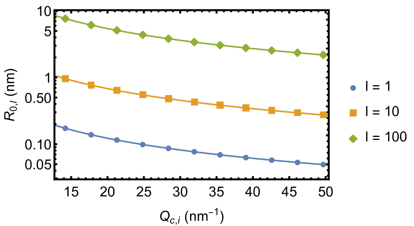
A.K. acknowledges the support of the Czech Science Foundation GACR under the Junior Star grant No. 23-05119M. R.H. was financially supported by the Spanish Ministry of Science and Innovation under the María de Maeztu Units of Excellence Program (CEX2020-001038-M/MCIN/AEI/10.13039/501100011033) and the Project PID2021-123949OB-I00. J.A. acknowledges the Spanish Ministry of Economy, Industry and Competitiveness (project PID2019-107432GB-I00). M.K.S. acknowledges support from the Macquarie University Research Fellowship scheme (MQRF0001036) and the Australian Research Council Discovery Early Career Researcher Award DE220101272.Appendix A VEB radius as a function of aperture size and OAM
In Fig. 8 we evaluate the dependence of the effective VEB radius for different forming aperture sizes and OAM.
Appendix B Note: Classical electric and magnetic current components
As we showed in the main text, we can find that the approximate electric current can be equivalently replaced by two sources and
| (46) |
However, we note that especially for larger or for probed structures with dimensions comparable to the vortex focus, the loss probability calculated using this model can differ both qualitatively and quantitatively from the rigorous approach, i.e. using the overlap integral in Eq. (5) within the quantum-mechanical description of the VEBs. We also note that an alternative magnetic current deduced from an effective spiralling electric current, as presented in Ref. Mohammadi et al. (2012), is expressed as , which involves an additional factor in their expression, as compared to Eq. (46), yielding several orders of magnitude larger values for the magnetic field current amplitude.
Appendix C Numerical calculations of (VEB-)EELS in Comsol Multiphysics
We utilize the Radio Frequency toolbox of Comsol Multiphysics software where we solve the wave equation for the total electric and magnetic field in the frequency domain with electric and magnetic current sources. We perform the calculations in a 3D simulation domain in the Cartesian coordinate system . The simulation domain includes the nanostructure characterized by a dielectric response , a straight line representing the electron’s trajectory, a simulation domain (typically a block) surrounding the nanostructure characterized by and Perfectly Matched Layers (PML) with Cartesian symmetry that help to attenuate the electric field at the boundaries of the simulation domain and prevent unphysical field reflections from the boundaries.
We apply the Free Tetrahedral mesh with refined elements in areas of high field concentration and gradients, typically close to the electron’s trajectory and nanostructures. We allow for an increase of the size of the mesh elements towards outer boundaries of the simulation domain. The area of PML is meshed by 5-10 Swept layers. The maximal allowed elements’ dimensions depend on the simulated energy region and thus on the typical wavelengths involved. We typically use fractions of the typical wavelength for the largest elements.
The electric current density component assigned to either conventional or vortex electron beam is implemented as line Edge Current, whereas the magnetic current is given by line Magnetic Current, as expressed in Eq. (28). The (VEB)-EEL probability is evaluated from 3D calculations according to Eq. (30) and Eq. (31) directly with this software using an Edge Probe, Integral along the electron’s trajectory between the boundaries at and .
All simulations are performed twice: with corresponding to the probed structure and then with everywhere, so that only the field of the electron is present, preserving the same discretization of the geometrical domains. Afterwards, the loss probability obtained from these two calculations is subtracted to obtain only the contribution coming from the induced field arising from the interaction of the electron beam with the nanostructure and to correct for the finite length of the electron’s trajectory and non-zero values of the fast electron’s field at the boundaries of the simulation domain Wiener et al. (2013); Raza et al. (2014); Govyadinov et al. (2017).
Appendix D Electron interacting with a dielectric cylinder
We adapt the expressions from Ref. Walsh (1991) for the electromagnetic field expressed in cylindrical coordinates for an electron beam moving in vacuum, parallel to an infinite dielectric cylinder along the axis. The cylinder has a radius and the electron beam is positioned at radial distance from the center of the cylinder.
The electric and magnetic field components, produced by the fast electron moving in vacuum, in cylindrical coordinates, and Fourier-transformed in the space are:
where and are the modified Bessel functions of the first and the second kind, respectively, of order , and is the Heaviside step function. We also defined . The components of the induced electric and magnetic field inside the cylinder () characterized by a dielectric function are:
whereas the induced electric and magnetic fields outside the cylinder () in vacuum are:
In the above expressions we assumed only solutions not diverging at and at infinity, and we also defined and . The unknown coefficients , , and are obtained by imposing boundary conditions at the boundaries of the cylinder:
| (47a) | ||||
| (47b) | ||||
| (47c) | ||||
| (47d) | ||||
By using the transformation in Eq. (26) we can obtain the electric and magnetic field produced in the presence of the cylinder due to the magnetic current component with the unknown coefficients redefined to , , and , that can be evaluated by applying the same boundary conditions as in Eqs. (47). The loss probability per unit trajectory due to the electric and magnetic current is then given by Eq. (43) and Eq. (44), respectively.
References
- Egerton (2011) R. F. Egerton, Electron energy-loss spectroscopy in the electron microscope (Springer Science & Business Media, 2011).
- García de Abajo (2010) F. J. García de Abajo, “Optical excitations in electron microscopy,” Rev. Mod. Phys. 82, 209–275 (2010).
- Nelayah et al. (2007) J. Nelayah, M. Kociak, O. Stéphan, F. J. García de Abajo, M. Tencé, L. Henrard, D. Taverna, I. Pastoriza-Santos, L. M. Liz-Marzán, and C. Colliex, “Mapping surface plasmons on a single metallic nanoparticle,” Nat. Physics 3, 348–353 (2007).
- Lagos et al. (2017) M. J. Lagos, A. Trügler, U. Hohenester, and P. E. Batson, “Mapping vibrational surface and bulk modes in a single nanocube,” Nature 543, 529–532 (2017).
- Govyadinov et al. (2017) A. A. Govyadinov, A. Konečná, A. Chuvilin, S. Vélez, I. Dolado, A. Y. Nikitin, S. Lopatin, F. Casanova, L. E. Hueso, J. Aizpurua, and R. Hillenbrand, “Probing low-energy hyperbolic polaritons in van der Walls crystal with an electron microscope,” Nat. Commun. 8, 95 (2017).
- Giannini et al. (2011) V. Giannini, A. I. Fernández-Domínguez, S. C. Heck, and S. A. Maier, “Plasmonic nanoantennas: Fundamentals and their use in controlling the radiative properties of nanoemitters,” Chem. Rev. 111, 3888–3912 (2011).
- Pelton et al. (2008) M. Pelton, J. Aizpurua, and G. Bryant, “Metal-nanoparticle plasmonics,” Laser Photonics Rev. 2, 136–159 (2008).
- Kuznetsov et al. (2016) A. I. Kuznetsov, A. E. Miroshnichenko, M. L. Brongersma, Y. S. Kivshar, and B. Luk’yanchuk, “Optically resonant dielectric nanostructures,” Science 354, aag2472 (2016).
- Jahani and Jacob (2016) S. Jahani and Z. Jacob, “All-dielectric metamaterials,” Nat. Nanotechnol. 11, 23 (2016).
- Verre et al. (2019) R. Verre, D. G. Baranov, B. Munkhbat, J. Cuadra, M. Käll, and T. Shegai, “Transition metal dichalcogenide nanodisks as high-index dielectric mie nanoresonators,” Nat. Nanotechnol. (2019), 10.1038/s41565-019-0442-x.
- Evlyukhin et al. (2012) A. B. Evlyukhin, S. M. Novikov, U. Zywietz, R. L. Eriksen, C. Reinhardt, S. I. Bozhevolnyi, and B. N. Chichkov, “Demonstration of magnetic dipole resonances of dielectric nanospheres in the visible region,” Nano Lett. 12, 3749–3755 (2012).
- Albella et al. (2014) P. Albella, R. Alcaraz de la Osa, F. Moreno, and S. A. Maier, “Electric and magnetic field enhancement with ultralow heat radiation dielectric nanoantennas: Considerations for surface-enhanced spectroscopies,” ACS Photonics 1, 524–529 (2014).
- Cambiasso et al. (2017) J. Cambiasso, G. Grinblat, Y. Li, A. Rakovich, E. Cortés, and S. A. Maier, “Bridging the gap between dielectric nanophotonics and the visible regime with effectively lossless gallium phosphide antennas,” Nano Lett. 17, 1219–1225 (2017).
- Bakker et al. (2015) R. M. Bakker, D. Permyakov, Y. F. Yu, D. Markovich, R. Paniagua-Domínguez, L. Gonzaga, A. Samusev, Y. Kivshar, B. Luk’yanchuk, and A. I. Kuznetsov, “Magnetic and electric hotspots with silicon nanodimers,” Nano Lett. 15, 2137–2142 (2015).
- Habteyes et al. (2014) T. G. Habteyes, I. Staude, K. E. Chong, J. Dominguez, M. Decker, A. Miroshnichenko, Y. Kivshar, and I. Brener, “Near-field mapping of optical modes on all-dielectric silicon nanodisks,” ACS Photonics 1, 794–798 (2014).
- Miroshnichenko et al. (2015) A. E. Miroshnichenko, A. B. Evlyukhin, Y. F. Yu, R. M. Bakker, A. Chipouline, A. I. Kuznetsov, B. Luk’yanchuk, B. N. Chichkov, and Y. S. Kivshar, “Nonradiating anapole modes in dielectric nanoparticles,” Nat. Commun. 6, 8069 (2015).
- Frolov et al. (2017) A. Yu. Frolov, N. Verellen, J. Li, X. Zheng, H. Paddubrouskaya, D. Denkova, M. R. Shcherbakov, G. A. E. Vandenbosch, V. I. Panov, P. Van Dorpe, A. A. Fedyanin, and V. V. Moshchalkov, “Near-field mapping of optical Fabry-Perot modes in all-dielectric nanoantennas,” Nano Lett. 17, 7629–7637 (2017).
- Coenen et al. (2013) T. Coenen, J. van de Groep, and A. Polman, “Resonant modes of single silicon nanocavities excited by electron irradiation,” ACS Nano 7, 1689–1698 (2013).
- van de Groep et al. (2016) J. van de Groep, T. Coenen, A. A. Mann, and A. Polman, “Direct imaging of hybridized eigenmodes in coupled silicon nanoparticles,” Optica 3, 93–99 (2016).
- Liu et al. (2019) Q. Liu, S. C. Quillin, D. J. Masiello, and P. A. Crozier, “Nanoscale probing of resonant photonic modes in dielectric nanoparticles with focused electron beams,” Phys. Rev. B 99, 165102 (2019).
- Kfir et al. (2020) O. Kfir, H. Lourenço-Martins, G. Storeck, M. Sivis, T. R. Harvey, T. J. Kippenberg, A. Feist, and C. Ropers, “Controlling free electrons with optical whispering-gallery modes,” Nature 582, 46–49 (2020).
- Alexander et al. (2021) D. T. L. Alexander, V. Flauraud, and F. Demming-Janssen, “Near-field mapping of photonic eigenmodes in patterned silicon nanocavities by electron energy-loss spectroscopy,” ACS Nano 15, 16501–16514 (2021).
- Cihan et al. (2018) A. F. Cihan, A. G. Curto, S. Raza, P. G. Kik, and M. L. Brongersma, “Silicon mie resonators for highly directional light emission from monolayer mos 2,” Nat. Photonics 12, 284 (2018).
- Regmi et al. (2016) R. Regmi, J. Berthelot, P. M. Winkler, M. Mivelle, J. Proust, F. Bedu, I. Ozerov, T. Begou, J. Lumeau, H. Rigneault, M. F. García-Parajó, S. Bidault, J. Wenger, and N. Bonod, “All-dielectric silicon nanogap antennas to enhance the fluorescence of single molecules,” Nano Lett. 16, 5143–5151 (2016).
- Rutckaia et al. (2017) V. Rutckaia, F. Heyroth, A. Novikov, M. Shaleev, M. Petrov, and J. Schilling, “Quantum dot emission driven by mie resonances in silicon nanostructures,” Nano Lett. 17, 6886–6892 (2017).
- Schmidt et al. (2012) M. K. Schmidt, R. Esteban, J.J. Sáenz, I. Suárez-Lacalle, S. Mackowski, and J. Aizpurua, “Dielectric antennas-a suitable platform for controlling magnetic dipolar emission,” Opt. Express 20, 13636–13650 (2012).
- Vaskin et al. (2019) A. Vaskin, S. Mashhadi, M. Steinert, K. E. Chong, D. Keene, S. Nanz, A. Abass, E. Rusak, D.-Y. Choi, I. Fernandez-Corbaton, T. Pertsch, C. Rockstuhl, M. A. Noginov, Y. S. Kivshar, D. N. Neshev, N. Noginova, and I. Staude, “Manipulation of magnetic dipole emission from Eu3+ with mie-resonant dielectric metasurfaces,” Nano Lett. 19, 1015–1022 (2019).
- Bliokh et al. (2007) K. Y. Bliokh, Y. P. Bliokh, S. Savel’ev, and F. Nori, “Semiclassical dynamics of electron wave packet states with phase vortices,” Phys. Rev. Lett. 99, 190404 (2007).
- Lloyd et al. (2017) S. M. Lloyd, M. Babiker, G. Thirunavukkarasu, and J. Yuan, “Electron vortices: Beams with orbital angular momentum,” Rev. Mod. Phys. 89, 035004 (2017).
- Bliokh et al. (2017) K. Y. Bliokh, I. P. Ivanov, G. Guzzinati, L. Clark, R. Van Boxem, A. Béché, R. Juchtmans, M. A. Alonso, P. Schattschneider, F. Nori, and J. Verbeeck, “Theory and applications of free-electron vortex states,” Phys. Rep. 690, 1–70 (2017).
- Uchida and Tonomura (2010) M. Uchida and A. Tonomura, “Generation of electron beams carrying orbital angular momentum,” Nature 464, 737–739 (2010).
- McMorran et al. (2011) B. J. McMorran, A. Agrawal, I. M. Anderson, A. A. Herzing, H. J. Lezec, J. J. McClelland, and J. Unguris, “Electron vortex beams with high quanta of orbital angular momentum,” Science 331, 192–195 (2011).
- Béché et al. (2014) A. Béché, R. Van Bosem, G. Van Tendeloo, and J. Verbeeck, “Magnetic monopole field exposed by electrons,” Nat. Phys. 10, 26–29 (2014).
- Mafakheri et al. (2017) E. Mafakheri, A. H. Tavabi, P.-H. Lu, R. Balboni, F. Venturi, C. Menozzi, G. C. Gazzadi, S. Frabboni, A. Sit, R. E. Dunin-Borkowski, E. Karimi, and V. Grillo, “Realization of electron vortices with large orbital angular momentum using miniature holograms fabricated by electron beam lithography,” Appl. Phys. Lett. 110, 093113 (2017).
- Vanacore et al. (2019) G. M. Vanacore, G. Berruto, I. Madan, E. Pomarico, P. Biagioni, R. J. Lamb, D. McGrouther, O. Reinhardt, I. Kaminer, B. Barwick, H. Larocque, V. Grillow, E. Karimi, F. J. García de Abajo, and F. Carbone, “Ultrafast generation and control of an electron vortex beam via chiral plasmonic near fields,” Nat. Materials (2019), 10.1038/s41563-019-0336-1.
- Tavabi et al. (2020) A. H. Tavabi, H. Larocque, P.-H. Lu, M. Duchamp, V. Grillo, E. Karimi, R. E. Dunin-Borkowski, and G. Pozzi, “Generation of electron vortices using nonexact electric fields,” Phys. Rev. Res. 2, 013185 (2020).
- Guzzinati et al. (2013) G. Guzzinati, P. Schattschneider, K. Y. Bliokh, F. Nori, and J. Verbeeck, “Observation of the larmor and gouy rotations with electron vortex beams,” Phys. Rev. Lett. 110, 093601 (2013).
- Grillo et al. (2017) V. Grillo, T. R. Harvey, F. Venturi, J. S. Pierce, R. Balboni, F. Bouchard, G. C. Gazzadi, S. Frabboni, A. H. Tavabi, Z.-A. Li, R. E. Dunin-Borkowski, R. W. Boyd, B. J. McMorran, and E. Karimi, “Observation of nanoscale magnetic fields using twisted electron beams,” Nat. Commun. 8, 689 (2017).
- Verbeeck et al. (2010) J. Verbeeck, H. Tian, and P. Schattschneider, “Production and application of electron vortex beams,” Nature 467, 301–304 (2010).
- Lloyd et al. (2012) S. Lloyd, M. Babiker, and J. Yuan, “Quantized orbital angular momentum transfer and magnetic dichroism in the interaction of electron vortices with matter,” Phys. Rev. Lett. 108, 074802 (2012).
- Yuan et al. (2013) J. Yuan, S. M. Lloyd, and M. Babiker, “Chiral-specific electron-vortex-beam spectroscopy,” Phys. Rev. A 88, 031801 (2013).
- Rusz et al. (2016) Ján Rusz, Juan-Carlos Idrobo, and Linus Wrang, “Vorticity in electron beams: Definition, properties, and its relationship with magnetism,” Phys. Rev. B 94, 144430 (2016).
- Juchtmans et al. (2015) R. Juchtmans, A. Béché, A. Abakumov, M. Batuk, and J. Verbeeck, “Using electron vortex beams to determine chirality of crystals in transmission electron microscopy,” Phys. Rev. B 91, 094112 (2015).
- Verbeeck et al. (2018) J. Verbeeck, A. Béché, K. Müller-Caspary, G. Guzzinati, M. A. Luong, and M. Den Hertog, “Demonstration of a 2x2 programmable phase plate for electrons,” Ultramicroscopy 190, 58 – 65 (2018).
- Konečná and García de Abajo (2020) A. Konečná and F. J. García de Abajo, “Electron beam aberration correction using optical near fields,” Phys. Rev. Lett. 125, 030801 (2020).
- García de Abajo and Konečná (2021) F. J. García de Abajo and A. Konečná, “Optical modulation of electron beams in free space,” Phys. Rev. Lett. 126, 123901 (2021).
- Ugarte and Ducati (2016) D. Ugarte and C. Ducati, “Controlling multipolar surface plasmon excitation through the azimuthal phase structure of electron vortex beams,” Phys. Rev. B 93, 205418 (2016).
- Guzzinati et al. (2017) G. Guzzinati, A. Béché, H. Lourenco-Martins, J. Martin, M. Kociak, and J. Verbeeck, “Probing the symmetry of the potential of localized surface plasmon resonances with phase-shaped electron beams,” Nat. Commun. 8 (2017), 10.1038/ncomms14999.
- Zanfrognini et al. (2019) M. Zanfrognini, E. Rotunno, S. Frabboni, A. Sit, E. Karimi, U. Hohenester, and V. Grillo, “Orbital angular momentum and energy loss characterization of plasmonic excitations in metallic nanostructures in tem,” ACS Photonics 6, 620–627 (2019).
- Mohammadi et al. (2012) Z. Mohammadi, C. P. Cole P. Van Vlack, S. Hughes, J. Bornemann, and R. Gordon, “Vortex electron energy loss spectroscopy for near-field mapping of magnetic plasmons,” Opt. Express 20, 15024–15034 (2012).
- Asenjo-Garcia and García de Abajo (2014) A. Asenjo-Garcia and F. J. García de Abajo, “Dichroism in the interaction between vortex electron beams, plasmons, and molecules,” Phys. Rev. Lett. 113, 066102 (2014).
- Bialynicki-Birula and Bialynicka-Birula (2017) I. Bialynicki-Birula and Z. Bialynicka-Birula, “Relativistic electron wave packets carrying angular momentum,” Phys. Rev. Lett. 118, 114801 (2017).
- Barnett (2017) S. M. Barnett, “Relativistic electron vortices,” Phys. Rev. Lett. 118, 114802 (2017).
- Tang and Cohen (2010) Y. Tang and A. E. Cohen, “Optical chirality and its interaction with matter,” Phys. Rev. Lett. 104, 163901 (2010).
- Novotny and Hecht (2006) L. Novotny and B. Hecht, Principles of Nano-Optics (Cambridge University Press, New York, 2006).
- García de Abajo (1999) F. J. García de Abajo, “Relativistic energy loss and induced photon emission in the interaction of a dielectric sphere with an external electron beam,” Phys. Rev. B 59, 3095–3107 (1999).
- Palik (1998) E. D. Palik, Handbook of optical constants of solids, Vol. 3 (Academic Press, 1998).
- Fu et al. (2013) Y. H. Fu, A. I. Kuznetsov, A. E. Miroshnichenko, Y.F. Yu, and B. Luk’yanchuk, “Directional visible light scattering by silicon nanoparticles,” Nat. Commun. 4, 1527 (2013).
- Yan et al. (2015) J. Yan, P. Liu, Z. Lin, H. Wang, H. Chen, C. Wang, and G. Yang, “Directional fano resonance in a silicon nanosphere dimer,” ACS Nano 9, 2968–2980 (2015).
- Zywietz et al. (2015) U. Zywietz, M. K. Schmidt, A. B. Evlyukhin, C. Reinhardt, J. Aizpurua, and B. N. Chichkov, “Electromagnetic resonances of silicon nanoparticle dimers in the visible,” ACS Photonics 2, 913–920 (2015).
- Rybin et al. (2015) M. V. Rybin, D. S. Filonov, P. A. Belov, Y. S. Kivshar, and M. F. Limonov, “Switching from visibility to invisibility via fano resonances: theory and experiment,” Sci. Rep. 5, 8774 (2015).
- Holsteen et al. (2017) A. L. Holsteen, S. Raza, P. Fan, P. G. Kik, and M. L. Brongersma, “Purcell effect for active tuning of light scattering from semiconductor optical antennas,” Science 358, 1407–1410 (2017).
- Traviss et al. (2015) D. J. Traviss, M. K. Schmidt, J. Aizpurua, and O. L. Muskens, “Antenna resonances in low aspect ratio semiconductor nanowires,” Opt. Express 23, 22771–22787 (2015).
- Abujetas et al. (2015) D. R. Abujetas, R. Paniagua-Domínguez, and J. A. Sánchez-Gil, “Unraveling the janus role of mie resonances and leaky/guided modes in semiconductor nanowire absorption for enhanced light harvesting,” ACS Photonics 2, 921–929 (2015).
- Cao et al. (2009) L. Cao, J. S. White, J.-S. Park, J. A. Schuller, B. M. Clemens, and M. L. Brongersma, “Engineering light absorption in semiconductor nanowire devices,” Nat. Mater. 8, 643 (2009).
- Bendaña et al. (2011) X. Bendaña, A. Polman, and F. J. García de Abajo, “Single-photon generation by electron beams,” Nano Lett. 11, 5099–5103 (2011).
- Walsh (1991) C. A. Walsh, “An analytical expression for the energy loss of fast electrons travelling parallel to the axis of a cylindrical interface,” Phil. Mag. B 63, 1063–1078 (1991).
- Snitzer (1961) E. Snitzer, “Cylindrical dielectric waveguide modes,” J. Opt. Soc. Am. 51, 491–498 (1961).
- Tong et al. (2004) L. Tong, J. Lou, and E. Mazur, “Single-mode guiding properties of subwavelength-diameter silica and silicon wire waveguides,” Opt. Express 12, 1025–1035 (2004).
- García de Abajo and Kociak (2008) F. J. García de Abajo and M. Kociak, “Probing the photonic local density of states with electron energy loss spectroscopy,” Phys. Rev. Lett. 100, 106804 (2008).
- Verhart et al. (2014) N. R. Verhart, G. Lepert, A. L. Billing, J. Hwang, and E. A. Hinds, “Single dipole evanescently coupled to a multimode waveguide,” Opt. Express 22, 19633–19640 (2014).
- Yin et al. (2013) X. Yin, M. Schäferling, B. Metzger, and H. Giessen, “Interpreting chiral nanophotonic spectra: The plasmonic born-kuhn model,” Nano Lett. 13, 6238–6243 (2013).
- Ee et al. (2015) H.-S. Ee, J.-H. Kang, M. L. Brongersma, and M.-K. Seo, “Shape-dependent light scattering properties of subwavelength silicon nanoblocks,” Nano Lett. 15, 1759–1765 (2015).
- Lourenço-Martins et al. (2021) H. Lourenço-Martins, D. Gérard, and M. Kociak, “Optical polarization analogue in free electron beams,” Nat. Physics 17, 598–603 (2021).
- Wiener et al. (2013) A. Wiener, H. Duan, M. Bosman, A. P. Horsfield, J. B. Pendry, J. K. W. Yang, S. A. Maier, and A. I. Fernández-Domínguez, “Electron-energy loss study of nonlocal effects in connected plasmonic nanoprisms,” ACS Nano 7, 6287–6296 (2013).
- Raza et al. (2014) S. Raza, N. Stenger, A. Pors, T. Holmgaard, S. Kadkhodazadeh, J. B. Wagner, K. Pedersen, M. Wubs, S. I. Bozhevolnyi, and N. A. Mortensen, “Extremely confined gap surface-plasmon modes excited by electrons,” Nat. Commun. 5 (2014), 10.1038/ncomms5125.