Power-Efficient Silicon Nitride Thermo-Optic Phase Shifters for Visible Light
Abstract
We demonstrate power-efficient, thermo-optic, silicon nitride waveguide phase shifters for blue, green, and yellow wavelengths. The phase shifters operated with low power consumption due to a suspended structure and multi-pass waveguide design. The devices were fabricated on 200-mm silicon wafers using deep ultraviolet lithography as part of an active visible-light integrated photonics platform. The measured power consumption to achieve a phase shift (averaged over multiple devices) was 0.78, 0.93, 1.09, and 1.20 mW at wavelengths of 445, 488, 532, and 561 nm, respectively. The phase shifters were integrated into Mach-Zehnder interferometer switches, and % rise(fall) times of about 570(590) s were measured.
I Introduction
Integrated photonics for visible wavelengths is becoming the focus of a growing number of research efforts in recent years [1, 2, 3, 4, 5, 6, 7]. By adapting the tools and fabrication infrastructure developed for silicon (Si) photonics at telecommunication wavelengths, visible-light photonic circuits with 10 - 100’s of components have been demonstrated for neurophotonics [6, 8], beam scanners [9], and quantum information [10, 11] applications. Fabrication on 200- and 300-mm diameter Si wafers has been enabled by the development of low-loss silicon nitride (SiN) [1, 4] and aluminum oxide (Al2O3) [12, 5] waveguides. Despite the visible-light transparency of these materials and their compatibility with Si photonics fabrication [13, 14, 15, 16, 17], the development of efficient phase shifters based on these waveguide materials has remained challenging. Conventional SiN thermo-optic phase shifters have a power consumption to achieve a phase shift, , of about 20-30 mW, owing to the relatively low thermo-optic coefficient of SiN of K-1 [6, 18]. The thermo-optic coefficient of Al2O3 ( K-1 in [12]) is similar to that of SiN. Phase shifters based on thermally-tuned SiN microdisks and microrings have of mW at wavelengths of 488 and 530 nm [19, 20, 21]; however, the low power consumption is attained at the expense of increased wavelength and fabrication error sensitivity compared to non-resonant structures. SiN phase shifters with liquid crystal cladding are expected to have significantly lower power consumption and such devices have been demonstrated at a wavelength of nm [22, 23], but post-processing steps are required to apply and encapsulate the liquid crystal. Low-loss lithium niobate nanophotonic waveguides have been demonstrated at red and near-infrared wavelengths ( nm, nm), and ultra-low power phase shifters have been demonstrated at a wavelength of 850 nm [24]; however, the incompatibility of lithium niobate processing with standard silicon photonics fabrication limits the levels of integration that may be achieved.
Here, we present visible-light, power-efficient, SiN, thermo-optic phase shifters based on a suspended heater structure with folded waveguides. Suspended heaters enable the power-efficient generation of isolated hot spots on-chip [25], and the thermo-optic phase shift increases with the number of times a waveguide is passed through the suspended volume [26]. As the structure is non-resonant, operation over a wide wavelength range is possible, and here, we demonstrate 0.78, 0.93, 1.09, 1.20 mW at wavelengths of 445, 488, 532, and 561 nm. Efficient suspended and folded-waveguide thermo-optic phase shifters have been demonstrated with Si waveguides at telecommunication wavelengths in [25, 26, 27, 28, 29, 30]; however, to our knowledge, this is the first demonstration of such a phase shifter in the visible spectrum. The power efficiency is comparable to microring/microdisk (resonant) thermo-optic phase shifters [19, 20] and a record among non-resonant visible-light SiN thermo-optic phase shifters. The phase shifters were fabricated on 200-mm diameter Si wafers as part of our visible-light integrated photonics platform, which also includes passive SiN waveguide devices [4], high-efficiency bi-layer edge-couplers [31], and SiN-on-Si photodetectors [32].
II Thermo-optic phase shifter design
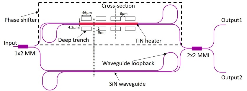
A schematic of the thermo-optic phase shifter is shown in Fig. 1(a). To facilitate characterization, the phase shifter was integrated into a Mach-Zehnder interferometer (MZI) with and multimode interference (MMI) couplers and nominally identical waveguide paths in each arm. The devices were designed in our visible-light integrated photonics platform using the 150 nm thick SiN waveguide layer deposited by plasma enhanced chemical vapor deposition (PECVD); the refractive index of the SiN was reported in [4].
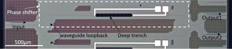
The phase shifter consisted of a suspended SiO2 bridge with a 500 m long titanium nitride (TiN) heater and folded SiN waveguides. The suspended region was formed by undercut etching of the Si substrate via rows of deep trenches (9 trenches per row); the gaps between the trenches formed SiO2 anchors for device robustness [28, 29]. The SiN waveguides looped through the suspended region 3 times using a folded structure with 60 m radius bends, and the total SiN waveguide length under the TiN heater was 1.5 mm.
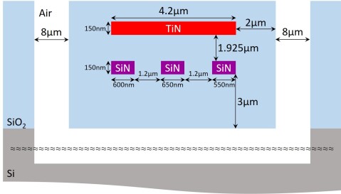
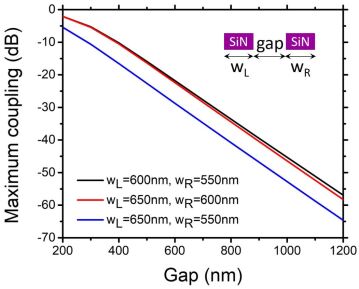
The waveguide dimensions were designed for the transverse-electric (TE) polarization. The designed cladding thicknesses, Fig. 1(b), ensured negligible TiN and Si substrate absorption; the computed TiN absorption loss at nm for a 550 nm wide waveguide was dB/cm. Since decreases with a narrower suspended region width, we applied the design strategy in [29] and selected dissimilar widths of 600, 650, and 550 nm for the 3 folded waveguides, such that the waveguide gap can remain small at 1.2 m without significant inter-waveguide coupling. The design was informed by the simulations in Fig. 1(c), which shows the simulated maximum coupling ratio between two waveguides at nm; the worst cross-coupling between the adjacent SiN waveguides is dB when the gap is 1.2 m.
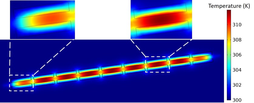
The thermo-optic phase shifter performance was modeled using COMSOL Multiphysics (for thermal simulations) and Lumerical MODE Solutions (for optical mode simulations). The simulations assumed a TiN resistance of 10 /sq, and thus, a heater resistance of 1190 . The undercut etch was modeled as elliptical channels in the Si substrate centered on the rows of deep trenches; the channels extended 8 m laterally and 18 m vertically from the edges of the deep trenches. The undercut etch was estimated from cross-section images of fabricated samples. The thermal simulations included a 2 mm thick air region above the device, and the bottom surface of the Si substrate was to set to a temperature of 300 K. The other boundaries of the simulated volume were set to be thermally insulating. The simulated temperature increase was highest in the suspended region, as shown in Fig. 1(d). For an applied current of 1 mA, equivalent to an electrical power dissipation of 1.19 mW, the calculated average temperature increase of the SiN waveguides under the TiN heater was 8.9 K. Next, the phase shift of the SiN waveguide was calculated using
| (1) |
where is the change of the SiN waveguide effective index with temperature, is the temperature change, and mm is the length of SiN waveguide under the TiN heater. To relate to the temperature change, we used the thermo-optic coefficients reported in [18]; K-1 for SiN and K-1 for SiO2, measured in the C band. The thermo-optic coefficients measured in [33] at wavelengths around 880 nm closely agree with these results. Via optical mode simulations, the calculated for K at nm, equivalent to a phase shift of 1.31. Therefore, the simulated of the phase shifter is 0.91 mW at 445 nm.
| Device |
|
|
|
|
|
|||||||||||
| PS1 | Yes | 3 | 1.5 | 4.2 | ||||||||||||
| PS2 | No | 3 | 1.5 | 4.2 | N.A. | |||||||||||
| PS3 | Yes | 7 | 6.9 | 10 |
Three phase shifter designs were investigated, and the parameters of each design are summarized in Table I. PS1 is the design described in this section and shown in Fig. 1. PS2 was nominally identical PS1 except for the lack of deep trenches and undercut etching. PS3 was investigated to explore the trade-off between the device insertion loss and tuning efficiency by increasing the length of the SiN waveguides under the TiN header; the 7 SiN waveguides under the heater had widths alternating among 600, 650, and 550 nm.
III Device fabrication and measurements
The thermo-optic phase shifters were fabricated on 200-mm diameter Si wafers at Advanced Micro Foundry (AMF) as part of our visible-light integrated photonics platform. The fabrication process, which includes multiple steps to define other devices in the platform, began with Si mesa patterning and doping to define Si photodiodes [32]. Next, PECVD SiO2 deposition and planarization was performed to define the bottom cladding of the waveguides. SiN waveguides (150 nm nominal thickness) were fabricated by SiN PECVD, deep ultraviolet (DUV) lithography, and reactive ion etching (RIE). Additional SiO2 and SiN deposition and patterning steps were performed to define a second SiN waveguide layer (75 nm nominal thickness) for bi-layer edge couplers [31]. Chemical mechanical polishing (CMP) was used for layer planarization. Following deposition of SiO2 top cladding for the waveguides, TiN heaters were defined, followed by 2 metal wiring layers (M1 and M2), vias (M1-M2, TiN-M2, Si photodiode - M1), and oxide openings for bond pads; similar to conventional Si photonic platforms for infared wavelengths [15]. Finally, deep trench and undercut etching were performed to define facets for edge couplers and the suspended SiO2 bridges of the thermo-optic phase shifters.
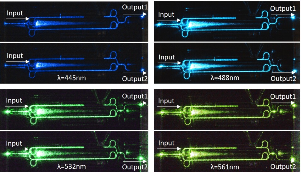
Figure 2(a) shows an optical micrograph of PS1 integrated into a MZI test structure. The input and output fiber-to-chip tapered edge couplers are labeled in the figure and have a width of 5.2 m at the facets. Optical micrographs of the MZI tested at blue, green, and yellow wavelengths are shown in Fig. 2(b); switching between the two outputs of the MZI by driving the phase shifter is demonstrated.
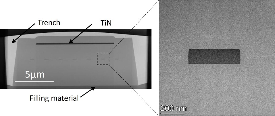
Figure 2(c) shows a cross-section transmission electron micrograph (XTEM) of PS3; the cross-section cut through the suspended SiO2 bridge and has the same orientation as the schematic in Fig. 1(b). The device measurements reported in this work focus on one wafer from the fabricated wafer lot, while the XTEM is from a second wafer. The only fabrication difference between these wafers was the SiO2 bottom cladding thickness of the SiN waveguides; 3 m for the first wafer and 3.25 m for the second. Investigation of one die from the second wafer yielded a similar PS1 performance to the first wafer. From the XTEM, the average separation between the SiN waveguide and the TiN heater was about 1.86 m, and the suspended region had a trapezoidal cross-section. The average separation between the edge SiN waveguide to the left and right edges of the suspended region was about 2 m, as designed. The average SiN waveguide width was about 100 nm narrower compared to the designed value, and correspondingly, the average SiN waveguide gap was about 100 nm larger than designed. The average SiN waveguide thickness in the XTEM was about 130 nm.
Device characterization was performed using Coherent OBIS LX (445 and 488 nm) and Sapphire FP (532 and 561 nm) lasers and a Newport 818-SL/DB photodetector connected to a Newport 2936-R optical power meter. Cleaved single-mode fibers (Nufern S405-XP) coupled light on-off the chips via the on-chip edge couplers, as in [4]. The input fiber had an inline fiber polarization controller to set the input polarization. DC drive voltages were applied to the devices from a sourcemeter (Keysight B2912A) via tungsten electrical probes contacting the on-chip pads, and the measured PS1 TiN heater resistance was about 1050 .
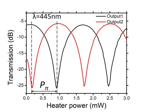
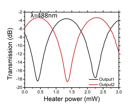
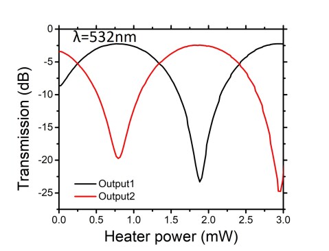
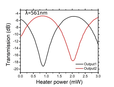
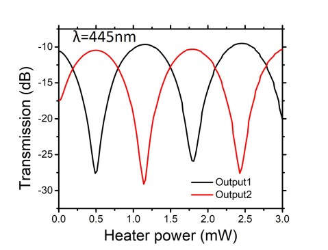
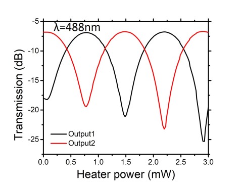
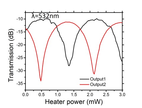
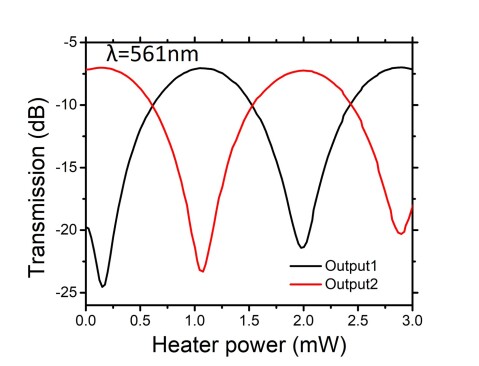
The phase shifters were integrated into MZI test structures to convert the applied phase shift into transmission changes at the MZI outputs. The measured PS1 MZI transmission as a function of heater power is shown in Fig. 3 at 445, 488, 532, and 561 nm. The power required to drive the MZI between the cross and thru states is of the phase shifter. The transmissions were normalized to those of a reference waveguide with the same edge coupler design as the MZI. The peaks and nulls of the transmission traces also indicate the insertion loss (IL) and extinction ratio (ER) of the MZI switch. The IL, ER, and were calculated from the first half-period of the tuning. Slight differences in the measurements from the two output ports were observed; likely due to waveguide loss variations between the MZI output waveguides, amplitude and phase errors of the MMI, and measurement error. Due to fiber alignment error and the waveguide loss of the reference waveguide being subtracted from the MZI loss during normalization, we estimate the IL measurements to be accurate to dB.
The measured results of PS1 are summarized in Table II. The phase shifter exhibited a low power consumption with measurements ranging from 0.79 - 1.22 mW and increasing with wavelength. The simulated values in Table II are in close agreement with the measurements. The increase of with wavelength is a result of the reduced optical confinement in the SiN at longer wavelengths and the lower thermo-optic coefficient of SiO2 relative to SiN. The ER was dB in all cases, indicating that the deep trenches in the phase shifter did not cause significant excess losses that would otherwise imbalance the MZI. Some dependence of the ER on the heater power was observed.
The IL of the PS1 MZI is a combination of the MMI losses and the waveguide losses in the MZI arms. Cutback measurements of 550 nm wide waveguides on one die indicated the waveguide losses were about 8.2, 7.0, 5.5, and 5.8 dB/cm at 445, 488, 532, and 561 nm, respectively. Simulations indicated minimum excess losses of 0.2 - 0.3 dB per MMI at green wavelengths and larger losses expected at 445 and 561 nm.
|
|
|
|
||||||||||||
|---|---|---|---|---|---|---|---|---|---|---|---|---|---|---|---|
| Output1 | Output2 | Output1 | Output2 | Output1 | Output2 | Simulation | |||||||||
| 445 | 6.1 | 6.5 | 19.8 | 19.0 | 0.79 | 0.82 | 0.91 | ||||||||
| 488 | 3.6 | 3.9 | 14.9 | 15.3 | 0.91 | 0.94 | 1.03 | ||||||||
| 532 | 2.5 | 2.4 | 21.0 | 17.3 | 1.09 | 1.09 | 1.17 | ||||||||
| 561 | 4.8 | 4.9 | 14.4 | 13.2 | 1.22 | 1.16 | 1.27 | ||||||||
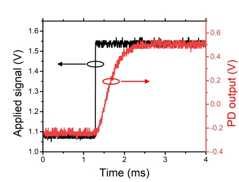
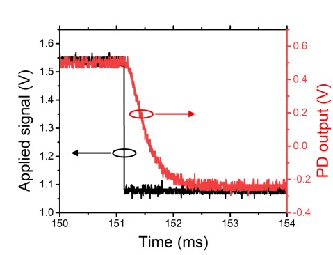
The rise and fall times of the PS1 MZI are presented in Fig. 4. A square wave voltage signal from a function generator (Tektronix AFG 31000) was applied to the device. The output optical signal was detected and read out on an oscilloscope (New Focus 2032, Keysight DSOX4054A). For Fig. 4(a), the ‘1’ level average voltage was about 0.500 V, and the ‘0’ level average voltage was about -0.239 V; for Fig. 4(b), the measured ‘1’ level average voltage was about 0.503 V, the measured ‘0’ level average voltage was about -0.239 V. The estimated % rise and fall times were about 570 s and 590 s, respectively.
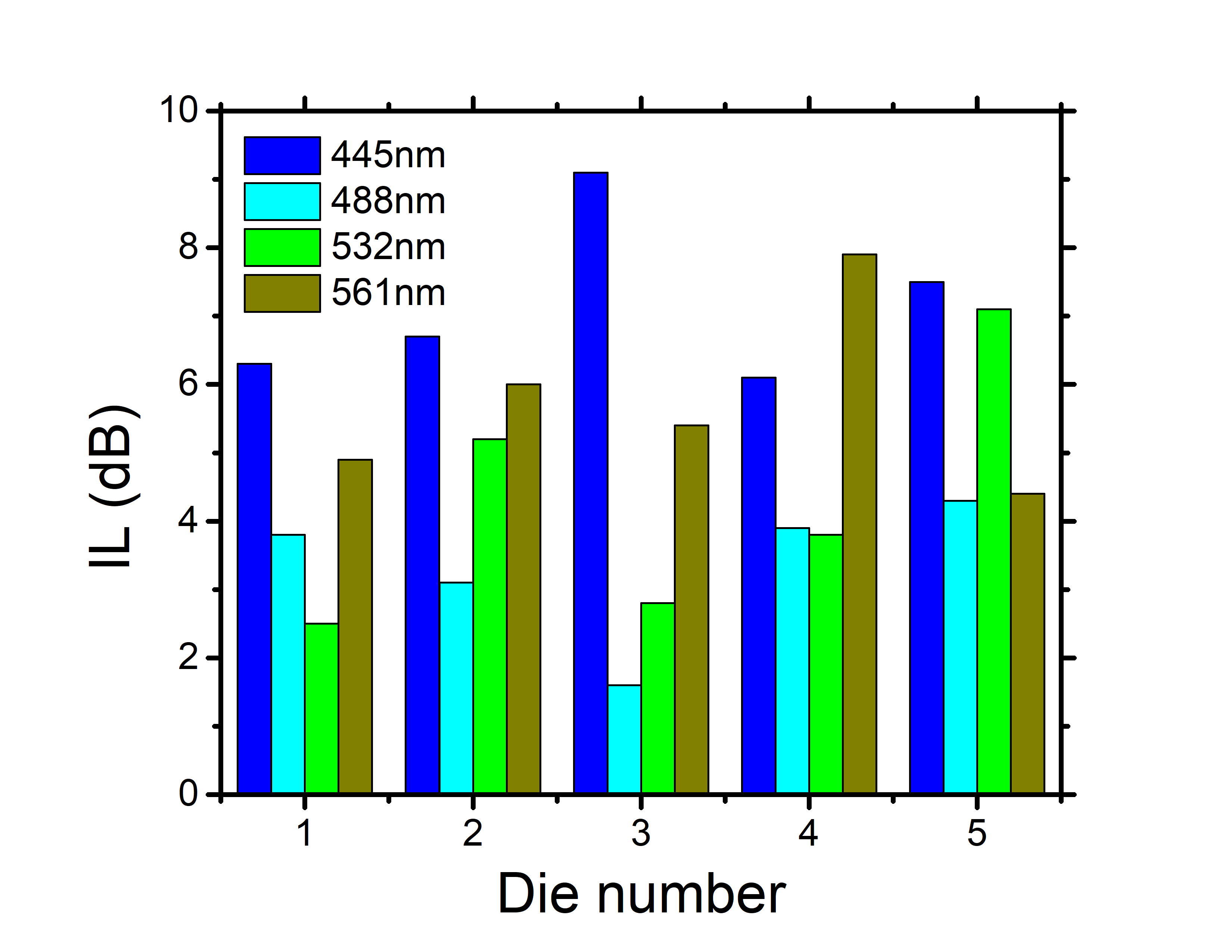
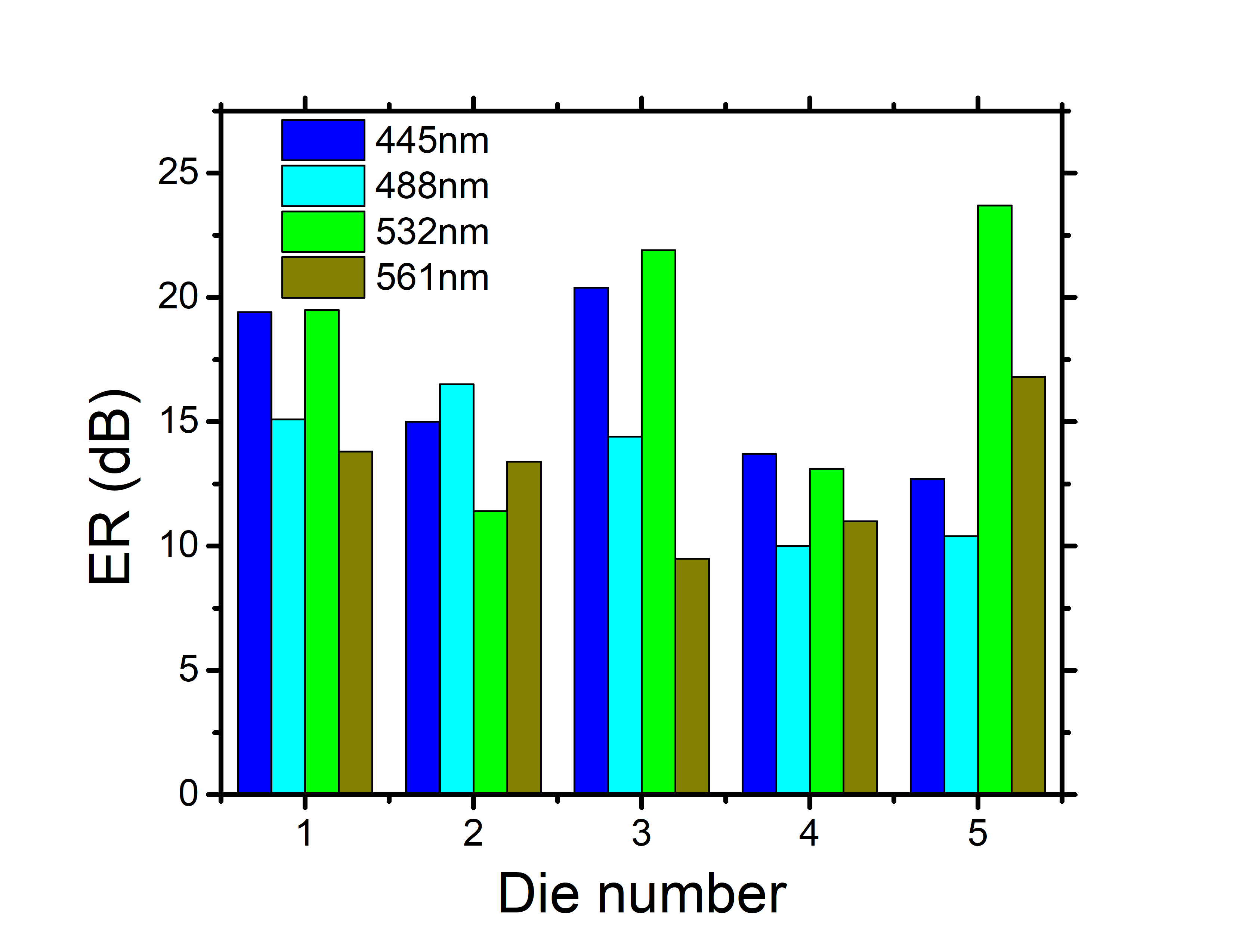
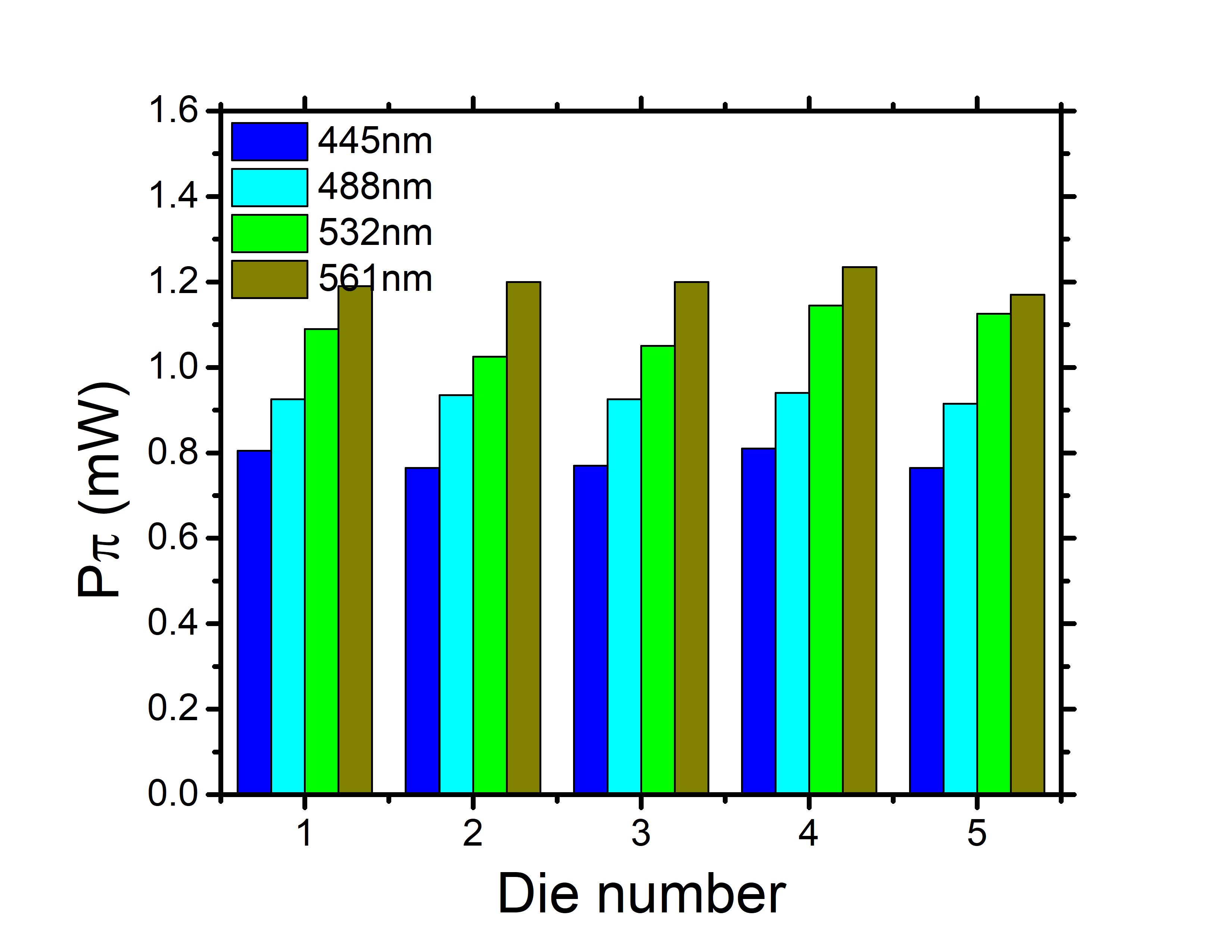
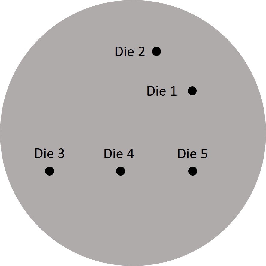
To check the repeatability of the results, we measured the tuning curves of the PS1 MZI on five different dies from the same wafer, and the results are summarized in Fig. 5(a)-(c), with the die locations shown in Fig. 5(d). The values in Fig. 5 were calculated from the average of the first half-period tuning of the MZI output ports 1 and 2. The average of PS1 across the dies was 0.78 mW, 0.93 mW, 1.09 mW, and 1.20 mW at 445, 488, 532, and 561 nm, respectively, and the variation in across the dies for each wavelength was mW. The average ER was 17.3 dB, 14.0 dB, 20.1 dB, and 13.6 dB at the same wavelengths, and the ER was dB in all cases. The average IL across the dies was 7.3 dB, 3.4 dB, 4.6 dB, and 5.9 dB at 445, 488, 532, and 561 nm, respectively; correspondingly, the maximum/minimum IL at each wavelength was 9.1/6.1 dB, 4.3/1.6 dB, 7.1/2.5 dB, 7.9/4.4 dB.
Contributions to the observed IL and its variation include measurement uncertainties (due to fiber alignment and laser power fluctuations), material and device loss across the wafer, and on-chip Fabry-Perot oscillations. The measurements were performed using 4 separate single-wavelength lasers with different spectral/power stabilities; the 532 nm laser had the largest observed fluctuations. Power fluctuations resulted in uncertainties in transmission measurements and polarization settings, both contributing to IL uncertainty; wavelength fluctuations affected the measured ER.
Due to the high mode confinement in the waveguides and the relatively small waveguide dimensions required for single- or few-mode operation in the visible spectrum, the waveguide losses are more sensitive to sidewall roughness scattering (compared to standard silicon photonics at infrared wavelengths). Similarly, the MMI losses are more sensitive to waveguide dimension errors. The device performance can likely be more consistent with optimization of the SiN etch process.
IV Discussion
To investigate the influence of design parameters, we compared the performance of PS1 against PS2 and PS3 (Table I). PS2, which did not have the deep trenches and undercut, had similar measured IL and ER as PS1 (comparing the MZI measurements); however, as expected, it had lower efficiency. The of PS2 was 15.9, 18.4, 22.2, and 23.0 mW at , 488, 532, and 561 nm respectively, about higher than PS1. The benefit was a much shorter % rise(fall) time of 34.5(33.5) s.
PS3 had 7 waveguide passes in the suspended heater (compared to 3 for PS1) with the aim of lower (at the expense of higher IL). PS3 simulations and measurements are detailed in the Appendix. The measured of PS3 was 0.65 mW at nm, about 81% of PS1. The small reduction in was accompanied by a large increase in insertion loss due to the increased waveguide length. As explained in the Appendix, the 15.4 m suspended region width (1.9 wider than that of PS1) resulted in an incomplete undercut in between the SiO2 anchors, and consequently, a reduced thermo-optic power efficiency.
Reductions in of PS1 may be possible through relatively simple design optimizations. Reducing the number of SiO2 anchors supporting the suspended region is expected to substantially increase the power efficiency [28], possibly at the expense of reduced mechanical robustness. In addition, according to the simulations in Fig. 1(c), our chosen waveguide gap of 1.2 m could be reduced to 0.6 m with a maximum crosstalk dB at nm, and the corresponding reduction in the suspended region volume is expected to increase the phase shifter power efficiency.
The insertion loss measurements in Section III include both the phase shifter and the MMIs of the MZI. Separate test structures to measure the loss of the MMIs were not available, and thus, it was not possible to directly measure the phase shifter loss from the MZI. Instead, as mentioned in Section III, we measured the waveguide loss of a 550 nm waveguide (the smallest of the 3 waveguide pass widths in the heater); the loss ranged from about 8 - 5.5 dB/cm from 445 - 561 nm, the total phase shifter waveguide length was 4.259 mm, and the resulting estimated phase shifter loss is 3.4 - 2.3 dB. The insertion loss of the phase shifter can be reduced by minimizing the waveguide length that is not in the heated suspended region. In this initial demonstration, a significant length of unnecessary routing waveguides was present in PS1. This is evident in Fig. 1(a); the waveguide bends for the loopbacks extend 521 m beyond the suspended region on each side. By removing this unnecessary waveguide length and the waveguide length used for routing from the MZI MMIs to and from the phase shifter, the minimum PS1 waveguide length is 3.335 mm; the estimated loss of this phase shifter is 2.7 - 1.9 dB from 445 - 561 nm.
The phase shifter loss can also be reduced by minimizing the waveguide scattering loss. With further optimization of the fabrication process, we expect the waveguide loss to be reduced to, at most, our previously demonstrated passive SiN waveguide platform losses (4 - 2 dB/cm for similar waveguide dimensions from 445 - 561 nm) [4]. With these reduced waveguide losses and the length optimization mentioned above, we expect the phase shifter loss could be about 1.3 - 0.7 dB from 445 - 561 nm.
V Conclusion
In summary, we have demonstrated power-efficient SiN thermo-optic phase shifters for the visible spectrum. The phase shifters had an ultra-low average of 0.78 mW at nm. The phase shifters were integrated into MZI switch test structures, and the measured 10% to 90% rise and fall times were about 570 s and 590 s, respectively. The devices operated at blue, green, and yellow wavelengths; the optical bandwidth was limited by the MMI couplers of the MZI. The phase shifters were fabricated on 200-mm diameter Si wafers as part of our visible-light integrated photonics platform. These demonstrated devices are monolithically integrated into silicon photonic circuits in contrast to phase shifters based on liquid crystals and electro-optic materials. They provide new possibilities to implement phase shifters in large-scale active photonic circuits in the visible spectrum.
|
|
|
|
||||||||||||
|---|---|---|---|---|---|---|---|---|---|---|---|---|---|---|---|
| Output1 | Output2 | Output1 | Output2 | Output1 | Output2 | Simulation | |||||||||
| 445 | 9.6 | 10.5 | 18.0 | 18.6 | 0.67 | 0.63 | 0.60 | ||||||||
| 488 | 6.9 | 6.8 | 11.3 | 12.6 | 0.73 | 0.73 | 0.68 | ||||||||
| 532 | 9.9 | 11.2 | 18.2 | 22.8 | 0.85 | 0.78 | 0.77 | ||||||||
| 561 | 7.1 | 7.0 | 17.5 | 16.3 | 0.90 | 0.93 | 0.83 | ||||||||
VI Appendix
PS3 had the same edge couplers and MMIs as PS1, but it had 7 SiN waveguides under the TiN heater, which was 10 m wide and 983.8 m long. The heater resistance used in simulations was 983.8 . The measured value was about 864 . The XTEM of PS3 is shown in Fig. 2(c). The tuning curves of PS3 at 4 different wavelengths are shown in Fig. 6. The IL of PS3 was generally higher than that of PS1 due to the increased waveguide length. The IL, ER, and of PS3 are summarized in Table III. The values in Table III are from the first half-period of the MZI tuning. With the same simulation conditions described in Section 2, the simulated of PS3 is 0.44 mW at nm. This is about 32% lower than the measured value. The discrepancy is likely due to the incomplete removal of Si under the suspended beam. Cross-section images of the suspended beams show that the undercut etch of the Si substrate had an elliptical shape and extended about 8 m laterally beyond each edge of the deep trench. The lateral extent of the undercut etch was wide enough to remove all the Si substrate under the suspended beam for PS1, but not directly between the SiO2 anchors for PS3. To model the incomplete undercut etch for PS3, we assumed 2m 2m Si posts connected the suspended beam to the Si substrate at regions directly between the SiO2 anchors. The resulting simulated of PS3 is 0.60 mW at 445 nm, close to the measured value. The simulations of PS3 with the incomplete undercut are summarized in Table III.
References
- [1] A. Z. Subramanian, P. Neutens, A. Dhakal, R. Jansen, T. Claes, X. Rottenberg, F. Peyskens, S. Selvaraja, P. Helin, B. Du Bois, K. Leyssens, S. Severi, P. Deshpande, R. Baets, and P. Van Dorpe, “Low-loss singlemode PECVD silicon nitride photonic wire waveguides for 532–900 nm wavelength window fabricated within a CMOS pilot line,” IEEE Photonics Journal 5, 2202809–2202809 (2013).
- [2] S. Romero-García, F. Merget, F. Zhong, H. Finkelstein, and J. Witzens, “Silicon nitride CMOS-compatible platform for integrated photonics applications at visible wavelengths,” Opt. Express 21, 14036–14046 (2013).
- [3] J. D. Domenech, M. A. G. Porcel, H. Jans, R. Hoofman, D. Geuzebroek, P. Dumon, M. van der Vliet, J. Witzens, E. Bourguignon, I. nigo Artundo, and L. Lagae, “Pix4life: photonic integrated circuits for bio-photonics,” in Integrated Photonics Research, Silicon and Nanophotonics, (Optical Society of America, 2018), p. ITh3B.1.
- [4] W. D. Sacher, X. Luo, Y. Yang, F.-D. Chen, T. Lordello, J. C. C. Mak, X. Liu, T. Hu, T. Xue, P. G.-Q. Lo, M. L. Roukes, and J. K. S. Poon, “Visible-light silicon nitride waveguide devices and implantable neurophotonic probes on thinned 200 mm silicon wafers,” Opt. Express 27, 37400–37418 (2019).
- [5] C. Sorace-Agaskar, D. Kharas, S. Yegnanarayanan, R. T. Maxson, G. N. West, W. Loh, S. Bramhavar, R. J. Ram, J. Chiaverini, J. Sage, and P. Juodawlkis, “Versatile silicon nitride and alumina integrated photonic platforms for the ultraviolet to short-wave infrared,” IEEE Journal of Selected Topics in Quantum Electronics 25, 1–15 (2019).
- [6] A. Mohanty, Q. Li, M. A. Tadayon, S. P. Roberts, G. R. Bhatt, E. Shim, X. Ji, J. Cardenas, S. A. Miller, A. Kepecs, and M. Lipson, “Reconfigurable nanophotonic silicon probes for sub-millisecond deep-brain optical stimulation,” Nature Biomedical Engineering 4, 223–231 (2020).
- [7] A. T. Mashayekh, T. Klos, D. Geuzebroek, E. Klein, T. Veenstra, M. Büscher, F. Merget, P. Leisching, and J. Witzens, “Silicon nitride PIC-based multi-color laser engines for life science applications,” Opt. Express 29, 8635–8653 (2021).
- [8] W. D. Sacher, F.-D. Chen, H. Moradi-Chameh, X. Luo, A. Fomenko, P. Shah, T. Lordello, X. Liu, I. F. Almog, J. N. Straguzzi, T. M. Fowler, Y. Jung, T. Hu, J. Jeong, A. M. Lozano, P. G.-Q. Lo, T. A. Valiante, L. C. Moreaux, J. K. S. Poon, and M. L. Roukes, “Implantable photonic neural probes for light-sheet fluorescence brain imaging,” Neurophotonics 8, 1 – 26 (2021).
- [9] C. V. Poulton, M. J. Byrd, M. Raval, Z. Su, N. Li, E. Timurdogan, D. Coolbaugh, D. Vermeulen, and M. R. Watts, “Large-scale silicon nitride nanophotonic phased arrays at infrared and visible wavelengths,” Opt. Lett. 42, 21–24 (2017).
- [10] R. J. Niffenegger, J. Stuart, C. Sorace-Agaskar, D. Kharas, S. Bramhavar, C. D. Bruzewicz, W. Loh, R. T. Maxson, R. McConnell, D. Reens, G. N. West, J. M. Sage, and J. Chiaverini, “Integrated multi-wavelength control of an ion qubit,” Nature 586, 538 – 542 (2020).
- [11] K. K. Mehta, C. Zhang, M. Malinowski, T.-L. Nguyen, M. Stadler, and J. P. Home, “Integrated optical multi-ion quantum logic,” Nature 586, 533 – 537 (2020).
- [12] G. N. West, W. Loh, D. Kharas, C. Sorace-Agaskar, K. K. Mehta, J. Sage, J. Chiaverini, and R. J. Ram, “Low-loss integrated photonics for the blue and ultraviolet regime,” APL Photonics 4, 026101 (2019).
- [13] E. Timurdogan, Z. Su, R.-J. Shiue, C. V. Poulton, M. J. Byrd, S. Xin, and M. R. Watts, “APSUNY process design kit (PDKv3. 0): O, C and L band silicon photonics component libraries on 300mm wafers,” in 2019 Optical Fiber Communications Conference and Exhibition (OFC), (IEEE, 2019), pp. 1–3.
- [14] Q. Wilmart, H. El Dirani, N. Tyler, D. Fowler, S. Malhouitre, S. Garcia, M. Casale, S. Kerdiles, K. Hassan, C. Monat et al., “A versatile silicon-silicon nitride photonics platform for enhanced functionalities and applications,” Applied Sciences 9, 255 (2019).
- [15] W. D. Sacher, J. C. Mikkelsen, Y. Huang, J. C. C. Mak, Z. Yong, X. Luo, Y. Li, P. Dumais, J. Jiang, D. Goodwill, E. Bernier, P. G.-Q. Lo, and J. K. S. Poon, “Monolithically integrated multilayer silicon nitride-on-silicon waveguide platforms for 3-D photonic circuits and devices,” Proceedings of the IEEE 106, 2232–2245 (2018).
- [16] P. Absil, K. Croes, A. Lesniewska, P. De Heyn, Y. Ban, B. Snyder, J. De Coster, F. Fodor, V. Simons, S. Balakrishnan et al., “Reliable 50Gb/s silicon photonics platform for next-generation data center optical interconnects,” in 2017 IEEE International Electron Devices Meeting (IEDM), (IEEE, 2017), pp. 34–2.
- [17] Tower Semiconductor, https://towersemi.com/manufacturing/mpw-shuttle-program/.
- [18] A. Arbabi and L. L. Goddard, “Measurements of the refractive indices and thermo-optic coefficients of and using microring resonances,” Optics Letters 38, 3878–3881 (2013).
- [19] G. Liang, H. Huang, S. Shrestha, A. Mohanty, X. Ji, M. C. Shin, M. Lipson, and N. Yu, “Micron-scale, efficient, robust phase modulators in the visible,” in Conference on Lasers and Electro-Optics, OSA Technical Digest (Optical Society of America, 2019), (2019), p. JTh5B.4.
- [20] H. Huang, G. Liang, A. Mohanty, X. Ji, M. C. Shin, M. Lipson, and N. Yu, “Robust miniature pure-phase modulators at k = 488 nm,” in Conference on Lasers and Electro-Optics, OSA Technical Digest (Optical Society of America, 2020), (2020), p. STh1J.4.
- [21] N. Yu and G. Liang and H. Huang and A. Mohanty, X. Ji, M. Shin, M. Carter, S. Shrestha, M. Lipson, “Micron-scale, efficient, and robust phase modulators at visible wavelengths,” Proc. SPIE 11694, Photonic and Phononic Properties of Engineered Nanostructures XI, 1169407, (2021).
- [22] M. Notaros, M. Raval, J. Notaros, and M. R. Watts, “Integrated visible-light liquid-crystal phase modulator,” in Frontiers in Optics, (Optical Society of America, 2018), pp. FW6B–5.
- [23] J. Notaros, M. Notaros, M. Raval, and M. R. Watts, “Liquid-crystal-based visible-light integrated optical phased arrays,” in 2019 Conference on Lasers and Electro-Optics (CLEO), (IEEE, 2019), pp. 1–2.
- [24] B. Desiatov, A. Shams-Ansari, M. Zhang, C. Wang, and M. Lončar, “Ultra-low-loss integrated visible photonics using thin-film lithium niobate,” Optica 6, 380–384 (2019).
- [25] R. Kasahara, K. Watanabe, M. Itoh, Y. Inoue, and A. Kaneko, “Extremely low power consumption thermooptic switch (0.6 mW) with suspended ridge and silicon-silica hybrid waveguide structures,” in 2008 34th European Conference on Optical Communication, (2008), pp. 1–2.
- [26] A. Densmore, S. Janz, R. Ma, J. H. Schmid, D.-X. Xu, A. Delâge, J. Lapointe, M. Vachon, and P. Cheben, “Compact and low power thermo-optic switch using folded silicon waveguides,” Opt. Express 17, 10457–10465 (2009).
- [27] Q. Fang, J. F. Song, T.-Y. Liow, H. Cai, M. B. Yu, G. Q. Lo, and D.-L. Kwong, “Ultralow power silicon photonics thermo-optic switch with suspended phase arms,” IEEE Photonics Technology Letters 23, 525–527 (2011).
- [28] Z. Lu, K. Murray, H. Jayatilleka, and L. Chrostowski, “Michelson interferometer thermo-optic switch on SOI with a 50- power consumption,” IEEE Photonics Technology Letters 27, 2319–2322 (2015).
- [29] K. Murray, Z. Lu, H. Jayatilleka, and L. Chrostowski, “Dense dissimilar waveguide routing for highly efficient thermo-optic switches on silicon,” Opt. Express 23, 19575–19585 (2015).
- [30] D. Celo, D. J. Goodwill, J. Jiang, P. Dumais, M. Li, and E. Bernier, “Thermo-optic silicon photonics with low power and extreme resilience to over-drive,” in 2016 IEEE Optical Interconnects Conference (OI), (IEEE, 2016), pp. 26–27.
- [31] Y. Lin, J. C. C. Mak, H. Chen, X. Mu, A. Stalmashonak, Y. Jung, X. Luo, P. G.-Q. Lo, W. D. Sacher, and J. K. S. Poon, “Low-loss broadband bi-layer edge couplers for visible light,” Opt. Express 29, 34565–34576 (2021).
- [32] Y. Lin, Z. Yong, X. Luo, P. G.-Q. Lo, W. D. Sacher, and J. K. Poon, “Silicon nitride waveguide-integrated silicon photodiodes for blue light,” in CLEO: Science and Innovations, (Optical Society of America, 2021), p. SM1A.3.
- [33] A. W. Elshaari, I. E. Zadeh, K. D. Jöns, and V. Zwiller, “Thermo-optic characterization of silicon nitride resonators for cryogenic photonic circuits,” IEEE Photonics Journal 8, 1–9 (2016).