marginparsep has been altered.
topmargin has been altered.
marginparwidth has been altered.
marginparpush has been altered.
The page layout violates the ICML style.
Please do not change the page layout, or include packages like geometry,
savetrees, or fullpage, which change it for you.
We’re not able to reliably undo arbitrary changes to the style. Please remove
the offending package(s), or layout-changing commands and try again.
AnalogNets: ML-HW Co-Design of Noise-robust TinyML Models and Always-On Analog Compute-in-Memory Accelerator
Anonymous Authors1
Abstract
Always-on TinyML perception tasks in IoT applications require very high energy efficiency. Analog compute-in-memory (CiM) using non-volatile memory (NVM) promises high efficiency and also provides self-contained on-chip model storage. However, analog CiM introduces new practical considerations, including conductance drift, read/write noise, fixed analog-to-digital (ADC) converter gain, etc. These additional constraints must be addressed to achieve models that can be deployed on analog CiM with acceptable accuracy loss. This work describes AnalogNets: TinyML models for the popular always-on applications of keyword spotting (KWS) and visual wake words (VWW). The model architectures are specifically designed for analog CiM, and we detail a comprehensive training methodology, to retain accuracy in the face of analog non-idealities, and low-precision data converters at inference time. We also describe AON-CiM, a programmable, minimal-area phase-change memory (PCM) analog CiM accelerator, with a novel layer-serial approach to remove the cost of complex interconnects associated with a fully-pipelined design. We evaluate the AnalogNets on a calibrated simulator, as well as real hardware, and find that accuracy degradation is limited to 0.8%/1.2% after 24 hours of PCM drift (8-bit) for KWS/VWW. AnalogNets running on the 14nm AON-CiM accelerator demonstrate 8.58/4.37 TOPS/W for KWS/VWW workloads using 8-bit activations, respectively, and increasing to 57.39/25.69 TOPS/W with -bit activations.
Preliminary work. Under review by the Machine Learning and Systems (MLSys) Conference. Do not distribute.
1 Introduction
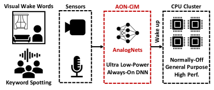
The origins of deep learning were with high-performance GPU hardware consuming hundreds of Watts of power and costing thousands of dollars. However, there is currently great interest in developing networks that can be deployed for inference tasks on constrained devices that can run autonomously on a few milliwatts of power and cost a few dollars, which is often referred to as TinyML. The applications for TinyML are numerous and varied, but including things like smart hearing aids Fedorov et al. (2020), machinery maintenance monitoring Banbury et al. (2021), human activity recognition Kodali et al. (2017) and so on. In this paper we focus on two popular always-on perception tasks: visual wake words (VWW) Chowdhery et al. (2019) and key-word spotting (KWS) Warden (2018), which turn on the more sophisticated ML functions when a person is in the camera frame or when a keyword is heard (Figure 1).
In many TinyML scenarios, the limitations of a constrained hardware platform introduce very significant challenges for DNN deployment. Typical microcontroller (MCU) hardware platforms are cheap ($1) and low power (10s mW) Fedorov et al. (2019). However, they often have very limited persistent storage (1 MB), memory (100s KB) and compute throughput (100s MOPS) Banbury et al. (2021). This limits the design of the DNN model in terms of: 1) number of parameters, 2) activation footprint, and 3) number of operations (ops) per inference. These three factors will largely determine the accuracy, latency and energy per inference that can be achieved by a given model.
The high compute and memory demands of DNN inference workloads has recently driven significant research interest in analog compute-in-memory (CiM) hardware platforms Zidan et al. (2018); Hamdioui et al. (2019); Li et al. (2019); Sebastian et al. (2020). The basic idea is to perform computation directly on data stored in on-chip memory, using analog signal processing. This potentially offers a big gain in energy efficiency compared to digital, due to: 1) removal of the weight memory read bottleneck, and 2) massive parallelism afforded by a dense array of millions of memory devices performing computation. Analog CiM has been demonstrated with a range of underlying memory technologies, including SRAM and non-volatile memory. Non-volatile memory (NVM) approaches are particularly relevant to TinyML applications, where we need single-chip solutions with all memory on-chip, and with low leakage. A recent phase change memory (PCM) based CiM chip Khaddam-Aljameh et al. (2021) demonstrated 10 TOPS/W at full utilization.
However, while analog CiM has been motivated as potentially offering orders of magnitude improvements in energy efficiency, its analog nature introduces a number of new challenges for practical DNN model design and training. Firstly, CiM introduces various types of noise in the weight storage, computation, and conversion from digital to analog and back again. This noise must be accounted for in the model training process to prevent degradation in runtime inference accuracy Garcia-Redondo et al. (2020); Joshi et al. (2020). Secondly, low-bitwidth quantization of models deployed on analog CiM platforms is also challenging, as it is essential to ensure high signal-to-noise (SNR) ratios to mitigate various noise processes. Finally, parameter-efficient TinyML models for CiM can not fully exploit some of the techniques extolled for MCU platforms, such as depthwise separable layers Howard et al. (2017), which must be expanded into a dense form for CiM. Therefore, systematic model-hardware co-design is required to deploy efficient, robust tinyML models on analog CiM platforms.
To date, research on CiM focuses on high throughput, fully-parallel hardware, with performance evaluated on either peak numbers (assuming 100% utilization) Khaddam-Aljameh et al. (2021), or on large benchmark models such as ResNet-50 Shafiee et al. (2016); Ankit et al. (2019); Jia et al. (2021), which also achieve high utilization. In contrast, this paper describes end-to-end model-hardware co-design of TinyML DNNs with an always-on PCM CiM accelerator. The main contributions are further summarized below:
-
•
AnalogNets, compact CiM-optimized TinyML DNNs for keyword spotting and visual wake words tasks. Architecture optimizations for analog noise robustness include removing small bottleneck layers and replacing depthwise layers with regular convolution.
-
•
Training Methodology for AnalogNets, incorporating noise injection for PCM noise, quantizers for finite DAC/ADC precision, and constrained optimization for fixed ADC gain constraints.
-
•
Accuracy Evaluation of trained AnalogNets on both a calibrated simulator and a real PCM prototype chip. The chip measurements show 95% and 85% accuracy for KWS and VWW during a 20-hour experiment. This is the first demonstration of TinyML deployed on analog PCM CiM hardware with competitive accuracy.
-
•
AON-CiM, a minimal area programmable CiM accelerator in 14nm with layer-serialized operation. Simulation results show 8.58/4.37 TOPS/W on AnalogNets KWS/VWW with 8-bit activations, up to 57.39/25.69 TOPS/W with 4-bit activations (6.1%/4.2% further accuracy degradation after 24 hours).
2 Related Work
Models for TinyML
Mounting interest in TinyML has sparked research on bespoke DNN models specifically targeting highly constrained hardware platforms. Early work by Gupta et al. (2017) and Kumar et al. (2017) proposed non-neural ML models to enable inference tasks on MCU hardware platforms with a few KBs of storage. Fedorov et al. (2019) demonstrated that CNNs are also feasible on MCUs, by designing a classifier for the CIFAR10-binary task with just KBs of Flash and RAM. This was achieved using neural architecture search (NAS) to find models that fit the severe model size constraints and still achieve good accuracy. Fedorov et al. (2020) demonstrate LSTMs optimized to fit on MCUs for smart hearing-aid applications. MCUNet (Lin et al., 2020) combines NAS and a custom MCU inference runtime to demonstrate ImageNet models with 70% accuracy on MCUs. MicroNets (Banbury et al., 2021) also used NAS to design state-of-the-art compact models for MCUs. This paper is the first to demonstrate TinyML models for analog CiM hardware.
Computation Noise and Noise-Robust Training
In Rekhi et al. (2019), noise due to analog computation is modeled as additive parameter noise with zero-mean Gaussian distribution and its variance is a function of the effective number of bits of the output of an analog computation. Similarly, Joshi et al. (2020) also model analog computation using an additive Gaussian on the parameters, with the variance calculated from the observed conductance distributions on their PCM devices. Some previous noise models have even included detailed device-level interactions, such as voltage drop across the analog array (Jain et al., 2018; Feinberg et al., 2018). Training neural networks with random noise (Srivastava et al., 2014; Noh et al., 2017; Li & Liu, 2016; Büchel et al., 2021) has been demonstrated to be highly effective at reducing overfitting and to increase robustness to adversarial attacks (Rakin et al., 2018). In this work, we employ an additive Gaussian noise model on the weights during training, similar to Rekhi et al. (2019); Joshi et al. (2020). Our noise-aware training method extends previous work to consider low-bitwidth data conversion, leveraging quantization-aware training Jacob et al. (2018).
Compute in Memory Hardware
Analog CiM schemes can be loosely categorized by the type of memory device employed. Many previous works demonstrate CiM using SRAM Valavi et al. (2019); Biswas & Chandrakasan (2018); Gonugondla et al. (2018); Jia et al. (2021); Lee et al. (2021); Sinangil et al. (2021). SRAM CiM has the significant advantage of availability in cutting-edge CMOS technologies, but is limited to storing two-levels per bitcell. A strong alternative is non-volative memory (NVM) (Shafiee et al., 2016; Ankit et al., 2019), such as flash (Merrikh-Bayat et al., 2017) or memristive devices, such as metal-oxide resistive RAM (ReRAM) (Hu et al., 2018; Yao et al., 2020), and phase-change memory (PCM) (Boybat et al., 2018; Ambrogio et al., 2018; Narayanan et al., 2021). Most NVM devices can store multiple levels per cell. For instance, PCM devices that can compute with an equivalent 8-bit precision Giannopoulos et al. (2018) have been demonstrated. In this paper we employ PCM-based CiM, modeled after Khaddam-Aljameh et al. (2021).
3 Analog CiM Background
This work focuses on NVM CiM arrays using phase-change memory (PCM) cells, specifically following a recent prototype in silicon by Khaddam-Aljameh et al. (2021).
3.1 Analog CiM Operation
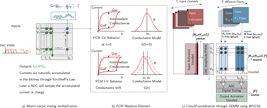
Matrix-vector operations from DNN inference are performed in parallel inside the CiM crossbar array (Figure 2). Weight values are stored in NVM cell array as conductances . Input activation vectors go through digital-to-analog converters (DACs), which generate pulse-width modulated (PWM) signals , applied to the crossbar source lines. PWM encoding avoids issues with current/voltage non-linearity in the NVM cells. A voltage pulse on a source line results in a momentary current flowing into the bitline from each connected unit cell, proportional to cell conductance . All source lines operate in parallel, with the currents from NVM cells summing on the bit lines simultaneously, following Kirchoff’s current law. Finally, an analog-to-digital converter (ADC) on the end of each bit line integrates the current over the activation pulses, to give a digital pre-activation output. Outside of the CiM array, bias, batch normalization and activation functions are applied in the digital domain, according to the network architecture. Note that, a differential NVM cell (two devices) and bitline, is used such that we can represent signed weights in .
3.2 Analog Non-Idealities
There are various non-idealities in Analog CiM, all of which result in noise, which can degrade inference accuracy. Below we discuss the three key practical considerations, which we later address to prevent accuracy loss.
3.2.1 NVM Cell Noise and Drift
Resistive PCM cells are each programmed to a value within the minimum and maximum conductance limits (Figure 2). The programming operation itself has limited precision due to variability and read noise Nandakumar et al. (2020). In addition, the effective stored value is also dependent on temperature and prone to drift over time Giannopoulos et al. (2018); Joshi et al. (2020). While the global component of this variation can be compensated to some extent by applying digital scaling factors on the ADC outputs Joshi et al. (2020), the device-to-device variability still causes noise that cannot be compensated, and degrades the computational precision over time.
At training time, we generically model this NVM noise as an additive zero-mean i.i.d. Gaussian error term on the weights of each layer , similar to Joshi et al. (2020). Then, at test time, we employ a detailed statistical PCM CiM model that accurately implements programming noise, 1/f noise and conductance drift, calibrated on the characterization of doped-Ge2Sb2Te5 (d-GST) mushroom-type PCM from a million device array integrated in 90nm CMOS technology Nandakumar et al. (2019).
3.2.2 DAC/ADC precision
The PWM DACs convert the input digital data to a series of unit voltage pulses on the source lines. Meanwhile, the ADCs sample the accumulated charge on the bitlines Yao et al. (2020); Khaddam-Aljameh et al. (2021); Narayanan et al. (2021). The DAC can be therefore abstracted as a quantizer on the input activations, assuming a given effective number of bits (ENOB). The DAC quantization ranges are set in digital, and therefore can be arbitrarily tuned per layer to properly address the variable dynamic range of the signals being converted. However, they must be kept constant throughout inference in order to avoid extra dynamic scaling circuits. Similarly, the ADC can be modeled as output activation ENOB quantization. However, the ADC quantization range cannot be arbitrarily tuned because its analog gain is usually fixed during a calibrating step.
3.2.3 ADC Gain
The last consideration is the ADC gain, the ADC analog gain stage must be calibrated to achieve a given conversion of bit-line charge to digital values Khaddam-Aljameh et al. (2021). Abstracted at the ML algorithm level (Section 4), this calibration can be represented as a scaling on the output activations prior to quantization. Because the time-consuming calibration must be performed for each ADC individually, it is not feasible to recalibrate the ADCs at inference time to achieve optimal quantization ranges per layer. Therefore, in this work, we require identical ADC gain across all layers.

4 AnalogNets: TinyML for CiM
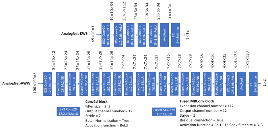
In this section, we build on previous TinyML models to meet the challenges of deploying DNNs on analog CiM hardware. We use the keyword spotting (KWS) and visual wake words (VWW) models from MicroNets Banbury et al. (2021). These state-of-the-art models are found by Neural Architecture Search (NAS) with constraints on model size, working memory and number of operations, to run efficiently on MCUs. We start with the smallest MicroNets models, more specifically MicroNet-KWS-S for KWS and MicroNet-VWW-2 (100100 resolution) for VWW.
4.1 Model Architectures
Depthwise Convolutions Are Not Suitable for CiM
Most state-of-the-art efficient DNNs feature depthwise convolution layers, due to their superior parameter efficiency. MicroNets models are no exception. Unfortunately, there are two issues with depthwise convolution on an analog CiM accelerator. First, depthwise layers are very inefficient when mapped onto a CiM array, as they must be expanded into a dense form with a non-zero diagonal, resulting in low hardware utilization (Figure 3, left). For example, when mapped to CiM, the second 33 depthwise convolution layer in MicroNet-KWS-S has local array utilization as low as . Second, the unused cells can also contribute additional noise into the bitline, which degrades the SNR (see remarks on small layers shortly).
Simulation of MicroNet-KWS-S on the PCM CiM simulator reveals unsatisfactory accuracy performance. The drop in accuracy is almost after a year of drift when employing 8-bit ADCs (see Appendix), compared to for the model we present in this paper. As a general design principle, DNNs designed for CiM should avoid depthwise convolutions. Therefore, in this paper we replace all depth-wise separable convolution blocks by regular 33 convolutions. For MicroNet-VWW-2 which is based on a MobileNetV2 backbone, the inverted bottleneck MBConv block thus becomes a fused-MBConv block Tan & Le . Although this change avoids the problems with depthwise convolution, it also introduces more parameters into the model. Therefore, to ensure the two models still fit on the same size CiM array (see Section 5), we have to remove the last parameter-heavy layer of 196 output channels from the KWS model.
Small Layers Are Bottlenecks
Efficient models may have narrow layers in the beginning of the network to keep the memory footprint low. But, we further found that these very narrow layers are bottlenecks that limit accuracy in the presence of noise. Narrow layers have few parameters and therefore are more sensitive to noise (in terms of variance). Layers with a small number of parameters may also not have enough redundancy to gain noise robustness during training. Theoretical work on information decay in noisy neural networks also supports avoiding narrow bottleneck layers Zhou et al. (2021). In our VWW model, we have identified two early layers that are bottlenecks, shown in Figure 3 (right), which result in degraded accuracy performance when tested on the CiM simulator. Therefore, to maintain accuracy, we remove these layers completely, which we find has little impact on model accuracy, model size and working memory. Table 1 shows the simulated accuracy of these two different model design choices (last and second last rows).
The two models developed are subsequently referred to as AnalogNet-KWS and AnalogNet-VWW. Their exact architectures can be found in the Appendix.
4.2 Model Training Methodology
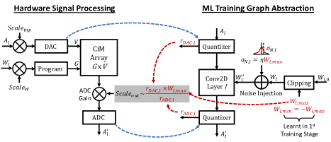
A CiM-specific training methodology is essential for these models. As we will show in Section 6, conventional TinyML models are not robust to analog CiM non-idealities, especially at low DAC/ADC bit precision. As discussed in Section 3, there are many different aspects of analog CiM hardware that must be properly accounted for during training. However, it is not practial to incorporate every detail of the hardware in the training process, so we develop a set of robust abstractions. For example, we simplify modeling of PCM noise (i.e., programming, temperature and drift effects) using Gaussian noise injection in weights. Joshi et al. (2020) described this approach in detail and demonstrated accuracy improvement on ResNet models measured on real PCM-based prototype hardware. Our work further develops this simple approach to train TinyML models adapted for inference on CiM with low-precision ADC/DACs. Figure 4 illustrates the process which abstracts the HW constraints and non-idealities to components in the ML model training graph. We next describe each component.
Noise Injection
At each forward pass, the weight noise in layer is drawn from an i.i.d. Gaussian distribution and added to the weights . The noise level is referenced to the maximum weight value in layer
| (1) |
where is a coefficient characterizing the noise power; a higher implies a reduced Signal-to-Noise Ratio (SNR). From a PCM CiM HW point of view, can be viewed as the ratio between combined average conductance noise standard deviation and the maximal conductance range on the PCM array Joshi et al. (2020). The maximal weight value obtained from regular neural network training is on the very tail of the distribution and highly susceptible to outlier influence. Therefore weight clipping is required to control the value of . We have
| (2) |
Joshi et al. (2020) compute clipping ranges dynamically, based on statistics of . Our approach is to use static clipping ranges during noise injection training, which we found is good for training stability. More details on calculation of clipping ranges can be found later in this section.
In terms of gradient computation, we treat the entire clipping and noise injection operation with a straight-through estimator (STE) Bengio et al. (2013). The gradients are computed with clipped and noise-perturbed weights, and are then applied to .
DAC/ADC Constraints
In Section 3 we described the role of DACs and ADCs in an analog CiM accelerator. From an ML training abstraction, we model the DACs and ADCs with simple effective number of bits (ENOB) quantizers. Quantization, whether for model weights or activations, is becoming ubiquitous in ML model training and there are many tools available. In the ML training graph (Figure 4), we model DACs and ADCs as separate quantization nodes. The input activation tensor is quantized by the DAC coming into the operator and the output pre-activation tensor is quantized by the ADC. Hardware constraints dictate that the ranges of these quantizers are symmetric, and we set the ENOB of the DAC to be 1-bit more than the ADC to accommodate the positivity of input activations after a ReLU activation function:
| (3) |
Setting the ranges for these quantizers, or equivalently choosing the scaling/gain factors for DAC/ADCs, is not easy especially because of the varying dynamic ranges between the signals on different filters and layers for a deep neural network with many layers. Furthermore, for low-precision DAC/ADCs, sub-optimal choices of these quantities leads to accuracy degradation. To address this problem, we adopt a fully differentiable approach to learn the ranges using gradient descent. Following a similar approach to Jain et al. (2019), the quantization function can be written as
| (4) |
The rounding operation rounds the number to its nearest integer and its gradient is calculated using the straight-through estimator (STE) Bengio et al. (2013). This quantization function is differentiable with respect to both and .
Figure 4 also describes the ADC gain constraint discussed in Section 3. The analog signal coming from the bitlines in the CiM array need to be scaled in the analog domain before being converted by the ADC. This analog scaling represents the ADC gain and is set at calibration time, and therefore it should be considered a constant across different layers. The scaling factor is related to the ranges of quantizers and maximum weight values to make sure that the ranges of ADCs and DACs are fully utilized. This constraint can be expressed as
| (5) |
and are respectively the maximum ranges of quantizers representing the DAC and the ADC in layer . is related to the noise injected into model weights by Equation 1. To eliminate one moving piece, we fix the value of during a two-stage training process.
In the first training stage, we train a model without any quantization nodes or noise injection and only with weight clipping in the range , where is the standard deviation of weights calculated with the unclipped weights . is updated every 10 time steps until the model is trained to convergence.
In the second training stage, we initialize the model with the trained weights from the first stage and compute the clipping ranges as , . and are then fixed throughout the training. We add noise injection and the quantization nodes representing the ADCs and DACs. We treat and as independent trainable parameters and initialize them at . Therefore and we take the absolute value of here to make sure that the ranges are all positive since may become negative during gradient descent. The gradient of can be computed as
| (6) |
where denotes the subgradient for the absolute value function. The gradients of are also slightly altered since there is now an extra differentiable path through . There are no gradients for as they are constant. Modern deep learning frameworks support automatic differentiation and can handle these gradient calculations seamlessly. We use TensorFlow to train our models.
5 AON-CiM Accelerator
Always-on (AON) accelerators operate alone while the remaining blocks in an SoC are unused and powered-down. Therefore, an AON accelerator must be self-contained, including all required memory. Below, we describe the fully-programmable AON-CiM accelerator used to evaluate the AnalogNets models.
5.1 Layer-Serial Approach
The conventional approach to mapping DNNs to CiM arrays is to map weights for each layer into a unique array, and then stream the activations through the arrays in a parallel/fully-pipelined style Dazzi et al. (2021). However, while this achieves the highest possible throughput, for TinyML applications, the fully-pipelined approach incurs area, power and control complexity overheads. In particular, two of these overheads are significant. First, fully-pipelined requires a large, high-bandwidth interconnect between the individual arrays. The interconnect is challenging to design, because the bandwidth required depends on the model architecture Dazzi et al. (2021). Second, layer-parallel requires each layer to be in a different CiM array. This increases the number of arrays and correspondingly the number of ADCs and DACs. Each array also must incorporate the compute required in between convolutions, such as activation functions, scaling, pooling etc, further increasing area.
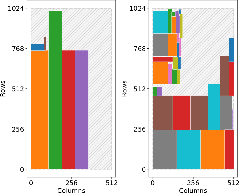
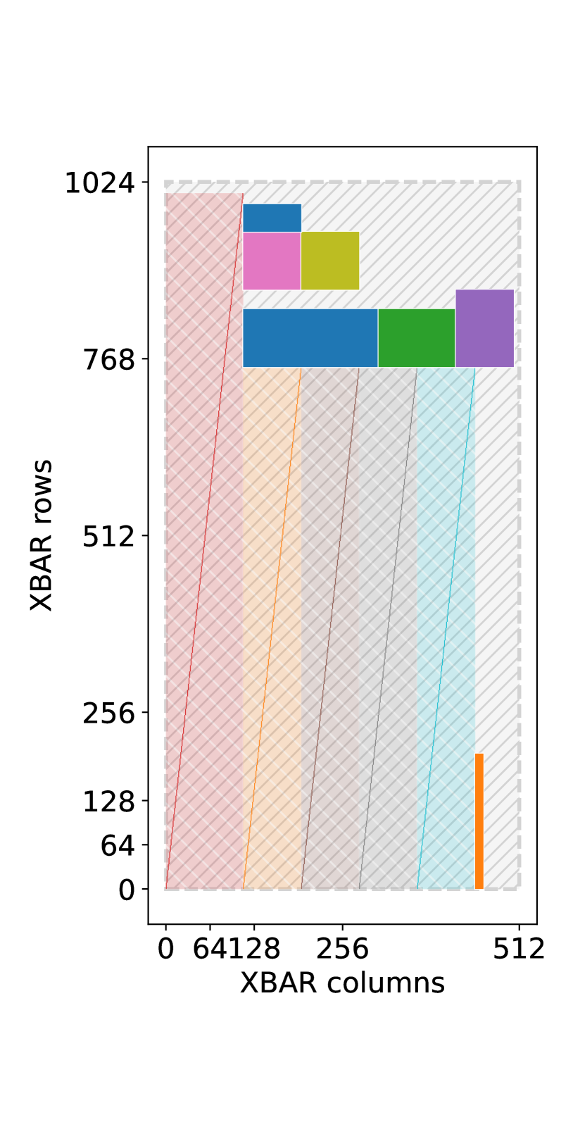
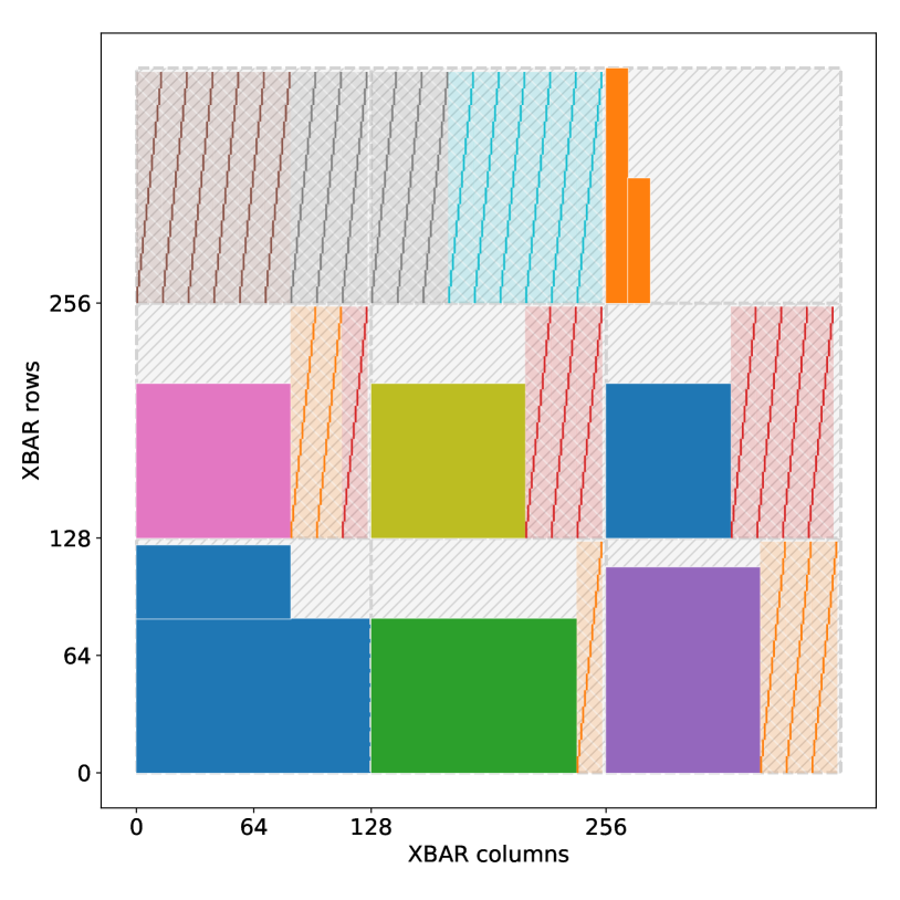
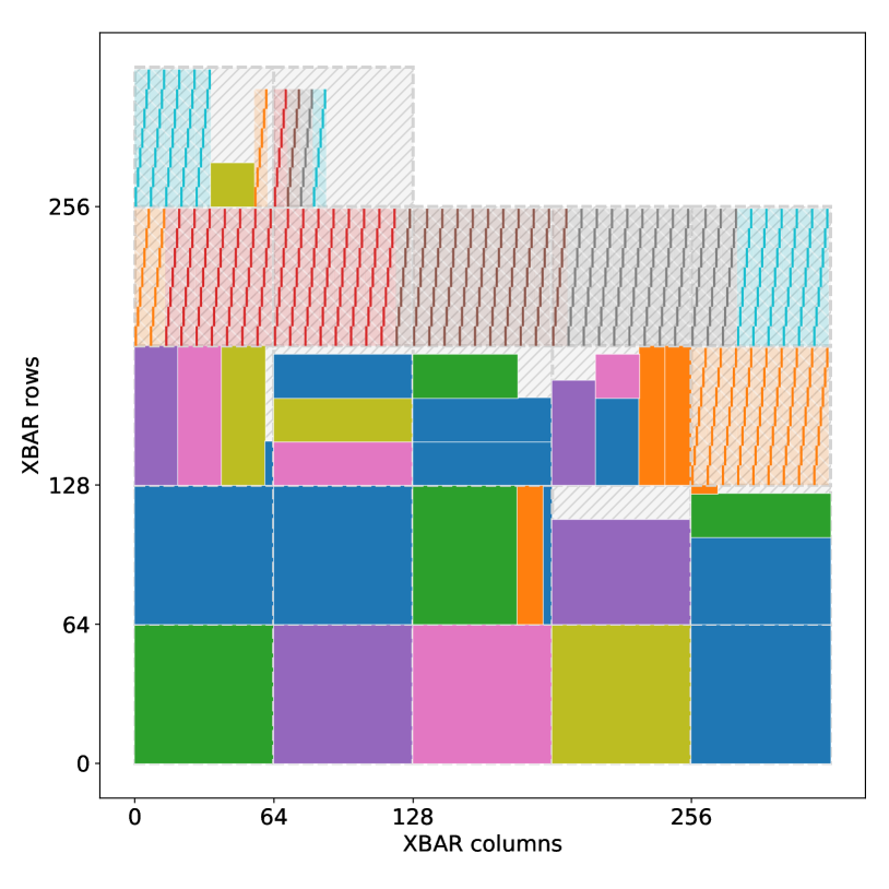
We propose an alternative approach of processing the network in a layer-serial fashion: process one layer at a time until it is complete, after which we start the next layer. Since only the weights associated with a single layer are used in any cycle, we do not need separate arrays for each layer, and we can store the whole model weights in the same CiM array. To illustrate this, Figure 6 gives mappings of the two AnalogNets models onto a single CiM array, with each layer represented by a colored box. With a single large array, the periphery cost of the DACs and ADCs is more heavily amortized, leading to improved energy efficiency. Furthermore, a programmable interconnect is no longer required, because the activations simply circulate from the output of the array to SRAM and from the SRAM to the input of the array.
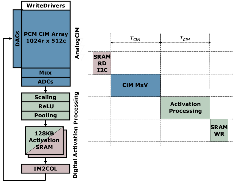
5.2 Accelerator Architecture
Figure 5 gives the AON-CiM accelerator architecture, consisting of two main parts: 1) PCM CiM array, and 2) the activation processing and storage pipeline.
Analog CiM Array
The array itself is based on Khaddam-Aljameh et al. (2021), but with 1024 rows and 512 columns to fit either of the AnalogNets models with some headroom for programmability. The tall aspect ratio is desirable, as ADCs consume more area than DACs, and besides, AnalogNets-KWS has tall layers, as shown in the mappings in Figure 6. Since we only use a subsection of the array for any given layer, we will rarely use all the DACs or ADCs at once. Therefore, to save power, we clock gate unused DACs and ADCs. To save area, we use a 4-input analog multiplexer on the bit-lines for a 4 reduction in ADCs (6% area benefit). We support 8/6/4-bit activation precision, as the CiM cycle time drops significantly due to the PWM DAC, which has exponential latency with bitwidth.
Activation Processing and Storage
Besides matrix-vector operations on the CiM array, we must also implement a number of mostly vector-wise operations on the pre-activation outputs from the array, including scaling, batch normalization, ReLU, pooling etc. The nominal 8-bit peak activation processing throughput required for this is 128 data words per 130ns array cycle, each of which requires two floating-point scalings and various integer functions depending on the layer type. However, supporting 4-bit activations without stalling the array requires the same 128 data words throughput at a 10ns array cycle time. Therefore, we add a digital datapath to meet the worst case 4-bit throughput, using an 800 MHz clock. Finally, the CiM input is fed with activations from the previous layer, stored in a double-buffered 128KB SRAM. A hardware IM2COL unit expands the activations before they are applied to the DACs in the CiM, using a small buffer and a programmable address generator. The activation processing, SRAM write/read and IM2COL are all pipelined, such that the array is never stalled (Figure 5), even in the challenging 4-bit case. Details of the control plane are omitted for brevity.
6 Results
6.1 Methodology
Model setup and training
We follow the data preprocessing and training setup of Banbury et al. (2021) to train baseline AnalogNet-KWS on the Google Speech Commands (V2) dataset and baseline AnalogNet-VWW on the Visual Wake Words dataset (100100 resolution). We also trained the same architectures using our HW-informed training methodology (Section 4.2). In the first training stage, AnalogNet-KWS (AnalogNet-VWW) was trained for 100 (200) epochs, with cosine learning rate decay and weight clipping. The second training stage uses the same numbers of epochs and learning rate (LR) decay schedule, but the initial LR is reduced to of its value in the first stage. An LR for the quantizer ranges is also introduced, with an exponentially decay from to . A gradient clipping threshold of is placed on the gradient for to stabilize its gradient update. We also exploit the stochastic “quantization noise” Fan et al. (2020) method to accelerate model training convergence at low bitwidths. The “quantization noise” probability of quantizers is set to .
Accuracy Evaluation
After training the models, the weights (clipped to [, ] and with no noise added), and the ranges of quantizers modelling the ADCs and DACs are transferred to a calibrated PCM CiM simulator, and further tested on a real 90nm PCM chip.
In the simulator, the clipped weights are rescaled to by dividing by and split into two arrays of equal size representing the positive and negative parts in conductances, which we denote as the target conductances . After rescaling, the programming noise is simulated. The programmed conductances, denoted by , are modeled using where . After the conductances are programmed, they drift over time, which also must be accounted for in the simulation Le Gallo et al. (2018). Drift at time , given the initial time of programming , can be modelled using , where is the drift coefficient that follows a normal distribution. Finally, when a matrix-vector multiplication is performed there will be instantaneous fluctuations on the hardware conductances due to the intrinsic noise from the PCM devices. PCM exhibits noise and random telegraph noise characteristics, which alter the effective conductance values used for computation. The final conductances in simulation follow a normal distribution , where with and .
Accuracy Experiments on Prototype PCM Hardware
Furthermore, we test model accuracy on a PCM-based prototype hardware chip, fabricated in 90 nm CMOS technology node Close et al. (2010). PCM devices are integrated into the chip via a key-hole process and doped Ge2Sb2Te5 is used as the phase-change material. The PCM array is organized as a crossbar with 512 source lines and 2048 bit lines, and an NMOS transistor serves as the PCM access device. The source lines and bit lines can only be serially addressed. A close-loop programming algorithm, as described in Joshi et al. (2020) is used to program the devices. A fixed voltage of 300 mV amplitude is applied to the source lines. The sensed current is integrated on a capacitor and the voltage is then converted to digital by 8-bit on-chip ADCs.
Hardware power, performance and area
The AON-CiM accelerator was modeled in a 14nm process technology. The digital part was evaluated using 14nm cell libraries and SRAM compilers, while the 14nm PCM CiM array was based on measurements reported by Khaddam-Aljameh et al. (2021). A bespoke layer-serial layer tiler was developed, along with a cycle accurate simulator. Together, these allow us to automatically map a given model to the AON-CiM accelerator and evaluate latency and energy.
6.2 AnalogNets Accuracy on PCM CiM Simulator
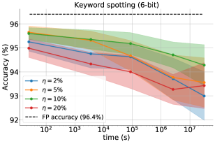
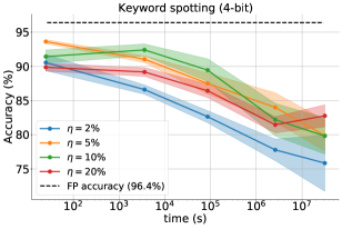
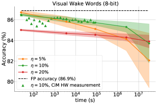
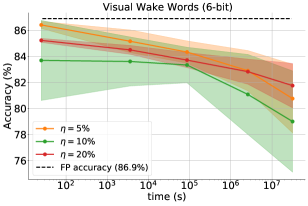
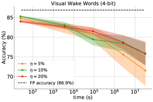
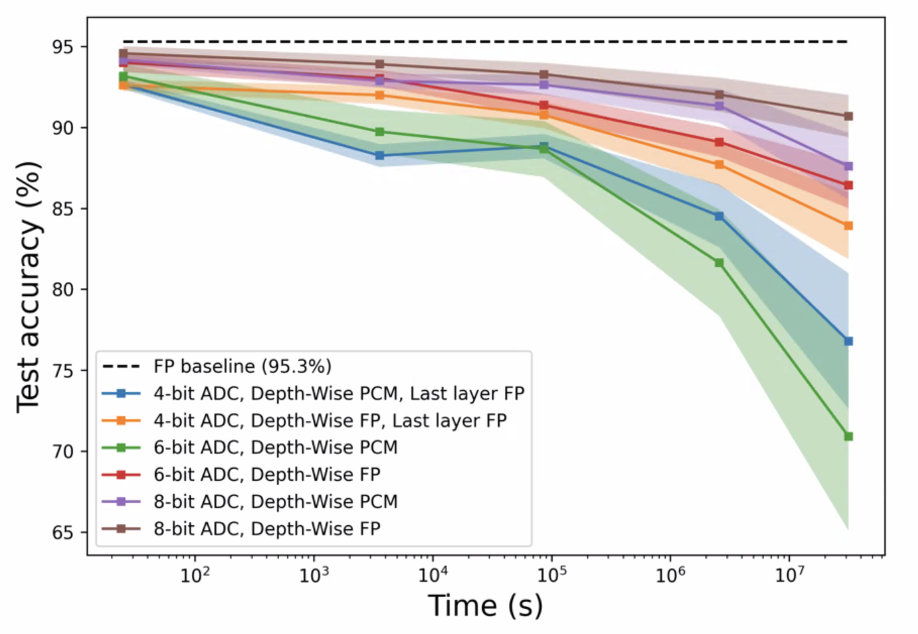
Models trained at varying noise levels were deployed on the simulator, configured with a 1024512 CiM array, such that no layers are split. Conductance drift in the PCM weights causes the model accuracy to degrade over time, even with the global drift compensation (GDC) Joshi et al. (2020). The simulator calculates accuracy after 25 seconds, 1 hour, 1 day, 1 month and 1 year of deployment. The means and standard deviations are computed from 25 runs.
6.2.1 Impact of Training Noise
We first explore sensitivity to training noise injection level , which is a training hyperparameter. The optimal value of may depend on the exact HW characteristics and the model itself. We show results for on KWS and for on VWW. Figure 7 summarizes the model accuracy performance over time for AnalogNet-KWS and AnalogNet-VWW at different activation precision. For AnalogNet-KWS, the best training noise level is around , while for AnalogNet-VWW, it is closer to , especially for lower activation bitwidths.
6.2.2 Quantization
On a logarithmic timescale, accuracy drops more sharply when the activation precision is reduced. On KWS, accuracy is maintained within of the digital floating point baseline for a year at 8-bit. While with a 6-bit ADC, that time is reduced to about a month. At 4-bit, the model can maintain accuracy for only about a day. On VWW, an accuracy drop of less than can be maintained for a year with 8-bit ADCs. At 6-bit, the accuracy drop can be maintained for about one month. At 4-bit, the model stays above for about a day. As we will see next, activation bitwidth has a big impact on latency and energy efficiency on the AON-CiM accelerator. Therefore, one could use activation precision to trade-off accuracy with hardware performance.
6.2.3 Ablation
Table 1 further shows an ablation study of the simulator results, demonstrating the advantage of our end-to-end training method. We compare with off-the-shelf models without special re-training, which drop to almost random level accuracy when tested on the simulator, and vanilla noise injection training Joshi et al. (2020). Vanilla noise injection can yield results close to our method at 8-bit activation precision, but becomes worse at lower precision. We also compare with the VWW model that has the small bottleneck layers added back (last row). The two models are trained in the same way with noise injection and ADC/DAC modeling. The VWW model with bottlenck layers, despite having more parameters than AnalogNet-VWW, has worse accuracy. Our end-to-end training methodology with ADC/DAC constraints also gives optimized ready-to-use DAC scaling parameters and ADC gains, which would otherwise need to be computed by sub-optimal empirical rules (see Appendix).
| KWS | |||||||||||
|---|---|---|---|---|---|---|---|---|---|---|---|
| Activation bitwidth | 8bit | 6bit | 4bit | ||||||||
| Baseline (no re-training) |
|
|
|
||||||||
| Noise injection () |
|
|
|
||||||||
|
|
|
|
||||||||
| VWW | |||||||||||
| Baseline (no re-training) |
|
|
|
||||||||
| Noise injection () |
|
|
|
||||||||
|
|
|
|
||||||||
| Bottleneck layers included |
|
|
|
||||||||
6.3 AnalogNets Validation on PCM CiM Test Chip
To simulate the model using CiM hardware, the weights are initially scaled to target conductances, which are then serially programmed into the hardware. After the conductances have been fully programmed, we wait for 20 hours while serially reading out the conductances at exponentially spaced points in time. The obtained conductances are then scaled down to the original weight magnitudes and used in the simulator to obtain the test accuracy. The results obtained using the PCM hardware are shown in Figure 7. The experiments are nicely aligned with the model simulations.
There are minor discrepancies between the simulator and the PCM hardware experiment. One reason for this is that our simulator does not take into account the convergence of the iterative programming algorithm. Although the overall convergence is above 99% for both models, a slightly lower convergence (98.5% ) is recorded for larger absolute wight values. Moreover, only a single experiment is evaluated while the simulations are repeated for 25 runs.
6.4 AON-CiM Accelerator Evaluation
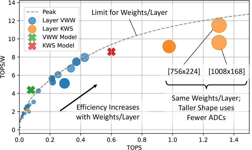
Table 2 summarizes the 14nm AON-CiM accelerator, including throughput and energy efficiency on the AnalogNets models. At 100% utilization, the single large CiM array achieves peak performance of TOPS and TOPS/W at 8/6/4-bit activation precision, respectively. The major gains at smaller bitwidths are due to the latency of the PWM DAC, which scales exponentially with bitwidth. However, real models do not use the whole array at once, so the achievable efficiency on a real model depends on the DNN architecture itself.
Figure 8 shows TOPS and TOPS/W for both individual layers and whole model performance of AnalogNets executing on the AON-CiM accelerator. We highlight two interesting trends. First, larger layers (shown by marker size) achieve higher TOPS and TOPS/W, because the DAC/ADC cost is amortized over more MACs. Second, even for layers with the same size, those with a tall aspect ratio have higher TOPS/W. This is because ADCs consume more energy than DACs, and taller layers require less ADCs for the same number of MACs. The limit on this aspect ratio benefit is shown as a dotted line for comparison, which some smaller layers meet. AnalogNet-KWS has a small number of tall layers, and hence achieves higher TOPS and TOPS/W than the smaller AnalogNet-VWW layers. Overall, the two models achieve throughput of and TOPS for KWS and VWW respectively, at bits activation precision. Their energy efficiency is and TOPS/W for KWS and VWW respectively, at bits activation precision.
6.5 Discussion
Finally, we briefly discuss our results in comparison with related work on TinyML for both analog CiM and MCUs.
TinyML on Analog CiM
Compared to previous work, AnalogNets demonstrates significantly higher accuracy. For example, on the KWS task, Dbouk et al. (2021) demonstrated a 65nm SRAM CiM test chip with 90.38% accuracy (91K parameters) on just 7 keywords. Guo et al. (2019) also report a 65nm SRAM CiM, which achieves 90.2% accuracy on 10 keywords. In contrast, AnalogNet-KWS achieves 95.6% (after 24h drift) on the full 12 keywords. This accuracy gap highlights the lack of research on model architectures and training methodologies for analog CiM.
TinyML on MCUs
MCUs are currently the commodity platform for TinyML. On the same KWS and VWW tasks, Banbury et al. (2021) report 48.6 mJ/inf. at 95.3%, and 196.2 mJ/inf. at 86.4%, respectively. While AnalogNets on AON-CiM accelerator show 8.2 uJ/inf. at 95.6% and 15.6 uJ/inf. at 85.7%, respectively. This is a very significant four orders of magnitude improvement in energy efficiency at comparable task accuracy. Therefore, although analog TinyML requires more complex model design and training, which is unlikely to be adopted for mainstream application, our work suggests that for severely energy constrained applications such as always-on TinyML, the effort is justified.
Future Work
Figure 8 shows that the size and shape of the layers has a huge impact on throughput and efficiency. Therefore, it may be possible to directly optimize the layer shapes and sizes, without increasing the overall model size, to attempt to achieve higher energy efficiency on the same AON-CiM hardware at similar accuracy.
| Technology | 14nm CMOS |
|---|---|
| Array Size | 1024 Rows 512 Columns (Mux4) |
| SRAM | 128 KB in Two Banks |
| Digital Ops | FP Scale, ReLU, Pooling, Add, IM2COL |
| Clock | : 130ns (8b), 34ns (6b), 10ns (4b) |
| Period | : 1.25ns |
| Chip Area | 3.2mm2 Total |
| 3.07mm2 CiM, 0.15mm2 Digital & SRAM | |
| Throughput | KWS: 0.6 TOPS, 7,762 inf/sec |
| (8b Act.) | VWW: 0.075 TOPS, 1,063 inf/sec |
| Energy Eff. | KWS: 8.58 TOPS/W, 8.22 J/inf |
| (8b Act.) | VWW: 4.37 TOPS/W, 15.6 J/inf |
7 Conclusion
Analog CiM hardware promises compelling improvements in energy efficiency, and is especially appealing for always-on TinyML tasks. However, analog CiM introduces numerous new practical challenges, such as various circuit non-idealities. It is therefore essential to address these challenges in both the design of the DNN architecture and the training of the model. In this paper, we described an ML-HW co-design approach to design AnalogNets: TinyML models optimized and trained specifically for analog CiM hardware, including aggressive quantization. AnalogNets demonstrate accuracy close to the digital floating point baselines, when tested on both a calibrated simulator and a real PCM testchip. We also described the AON-CiM accelerator, which introduces a novel layer-serial approach to minimize area for IoT applications. The combined effort gives close-to-digital model accuracy on a significantly more energy efficient hardware platform.
Acknowledgement
This work was supported in part by the European Union’s Horizon 2020 Research, Innovation Program through the project MNEMOSENE under Grant 780215.
References
- Ambrogio et al. (2018) Ambrogio, S., Narayanan, P., Tsai, H., Shelby, R. M., Boybat, I., di Nolfo, C., Sidler, S., Giordano, M., Bodini, M., Farinha, N. C., et al. Equivalent-accuracy accelerated neural-network training using analogue memory. Nature, 558(7708):60, 2018.
- Ankit et al. (2019) Ankit, A. et al. PUMA: A programmable ultra-efficient memristor-based accelerator for machine learning inference. In Proc. Intl. Conf. on Architectural Support for Programming Languages and Operating Systems, 2019.
- Banbury et al. (2021) Banbury, C., Zhou, C., Fedorov, I., Matas, R., Thakker, U., Gope, D., Janapa Reddi, V., Mattina, M., and Whatmough, P. Micronets: Neural network architectures for deploying tinyml applications on commodity microcontrollers. Proceedings of Machine Learning and Systems, 3, 2021.
- Bengio et al. (2013) Bengio, Y., Léonard, N., and Courville, A. Estimating or propagating gradients through stochastic neurons for conditional computation. arXiv preprint arXiv:1308.3432, 2013.
- Biswas & Chandrakasan (2018) Biswas, A. and Chandrakasan, A. P. Conv-sram: An energy-efficient sram with in-memory dot-product computation for low-power convolutional neural networks. IEEE Journal of Solid-State Circuits, 54(1):217–230, 2018.
- Boybat et al. (2018) Boybat, I., Le Gallo, M., Nandakumar, S., Moraitis, T., Parnell, T., Tuma, T., Rajendran, B., Leblebici, Y., Sebastian, A., and Eleftheriou, E. Neuromorphic computing with multi-memristive synapses. Nature communications, 9(1):2514, 2018.
- Büchel et al. (2021) Büchel, J., Faber, F., and Muir, D. R. Network insensitivity to parameter noise via adversarial regularization. CoRR, abs/2106.05009, 2021. URL https://arxiv.org/abs/2106.05009.
- Chowdhery et al. (2019) Chowdhery, A., Warden, P., Shlens, J., Howard, A., and Rhodes, R. Visual wake words dataset. arXiv preprint arXiv:1906.05721, 2019.
- Close et al. (2010) Close, G. F., Frey, U., Breitwisch, M., Lung, H. L., Lam, C., Hagleitner, C., and Eleftheriou, E. Device, circuit and system-level analysis of noise in multi-bit phase-change memory. In 2010 International Electron Devices Meeting, pp. 29.5.1–29.5.4, 2010. doi: 10.1109/IEDM.2010.5703445.
- Dazzi et al. (2021) Dazzi, M., Sebastian, A., Parnell, T., Francese, P. A., Benini, L., and Eleftheriou, E. Efficient pipelined execution of cnns based on in-memory computing and graph homomorphism verification. IEEE Transactions on Computers, 70(6):922–935, 2021. doi: 10.1109/TC.2021.3073255.
- Dbouk et al. (2021) Dbouk, H., Gonugondla, S. K., Sakr, C., and Shanbhag, N. R. A 0.44uj/dec, 39.9us/dec, recurrent attention in-memory processor for keyword spotting. IEEE Journal of Solid-State Circuits, 56(7):2234–2244, 2021. doi: 10.1109/JSSC.2020.3029586.
- Fan et al. (2020) Fan, A., Stock, P., Graham, B., Grave, E., Gribonval, R., Jegou, H., and Joulin, A. Training with quantization noise for extreme model compression. arXiv preprint arXiv:2004.07320, 2020.
- Fedorov et al. (2019) Fedorov, I., Adams, R. P., Mattina, M., and Whatmough, P. N. Sparse: Sparse architecture search for cnns on resource-constrained microcontrollers. In Proceedings of the Neural Information Processing Systems (NeurIPS) Conference 2019, 2019.
- Fedorov et al. (2020) Fedorov, I., Stamenovic, M., Jensen, C., Yang, L.-C., Mandell, A., Gan, Y., Mattina, M., and Whatmough, P. N. Tinylstms: Efficient neural speech enhancement for hearing aids. arXiv preprint arXiv:2005.11138, 2020.
- Feinberg et al. (2018) Feinberg, B., Wang, S., and Ipek, E. Making memristive neural network accelerators reliable. In 2018 IEEE International Symposium on High Performance Computer Architecture (HPCA), pp. 52–65. IEEE, 2018.
- Garcia-Redondo et al. (2020) Garcia-Redondo, F., Das, S., and Rosendale, G. Training DNN IoT Applications for Deployment On Analog NVM Crossbars. In 2020 Int. Jt. Conf. Neural Networks, pp. 1–8. IEEE, jul 2020. ISBN 978-1-7281-6926-2. doi: 10.1109/IJCNN48605.2020.9206822. URL https://ieeexplore.ieee.org/document/9206822/.
- Giannopoulos et al. (2018) Giannopoulos, I., Sebastian, A., Le Gallo, M., Jonnalagadda, V., Sousa, M., Boon, M., and Eleftheriou, E. 8-bit precision in-memory multiplication with projected phase-change memory. In 2018 IEEE International Electron Devices Meeting (IEDM), pp. 27.7.1–27.7.4, 2018. doi: 10.1109/IEDM.2018.8614558.
- Gonugondla et al. (2018) Gonugondla, S. K., Kang, M., and Shanbhag, N. A 42pj/decision 3.12 tops/w robust in-memory machine learning classifier with on-chip training. In 2018 IEEE International Solid-State Circuits Conference-(ISSCC), pp. 490–492. IEEE, 2018.
- Guo et al. (2019) Guo, R., Liu, Y., Zheng, S., Wu, S.-Y., Ouyang, P., Khwa, W.-S., Chen, X., Chen, J.-J., Li, X., Liu, L., Chang, M.-F., Wei, S., and Yin, S. A 5.1pj/neuron 127.3us/inference rnn-based speech recognition processor using 16 computing-in-memory sram macros in 65nm cmos. In 2019 Symposium on VLSI Circuits, pp. C120–C121, 2019. doi: 10.23919/VLSIC.2019.8778028.
- Gupta et al. (2017) Gupta, C., Suggala, A. S., Goyal, A., Simhadri, H. V., Paranjape, B., Kumar, A., Goyal, S., Udupa, R., Varma, M., and Jain, P. Protonn: Compressed and accurate knn for resource-scarce devices. In Proceedings of the 34th International Conference on Machine Learning - Volume 70, ICML’17, pp. 1331–1340. JMLR.org, 2017.
- Hamdioui et al. (2019) Hamdioui, S., Du Nguyen, H. A., Taouil, M., Sebastian, A., Gallo, M. L., Pande, S., Schaafsma, S., Catthoor, F., Das, S., Redondo, F. G., Karunaratne, G., Rahimi, A., and Benini, L. Applications of Computation-In-Memory Architectures based on Memristive Devices. In 2019 Des. Autom. Test Eur. Conf. Exhib., pp. 486–491. IEEE, mar 2019. ISBN 978-3-9819263-2-3. doi: 10.23919/DATE.2019.8715020. URL https://ieeexplore.ieee.org/document/8715020/.
- Howard et al. (2017) Howard, A. G., Zhu, M., Chen, B., Kalenichenko, D., Wang, W., Wey, T., Andreetto, M., and Adam, H. MobileNets: Efficient Convolutional Neural Networks for Mobile Vision Applications. CoRR, abs/1704.04861, 2017. URL http://arxiv.org/abs/1704.04861.
- Hu et al. (2018) Hu, M., Graves, C., Li, C., Li, Y., Ge, N., Montgomery, E., Davila, N., Jiang, H., Williams, R., Yang, J., et al. Memristor-based analog computation and neural network classification with a dot product engine. Advanced materials (Deerfield Beach, Fla.), 30(9), 2018.
- Jacob et al. (2018) Jacob, B., Kligys, S., Chen, B., Zhu, M., Tang, M., Howard, A., Adam, H., and Kalenichenko, D. Quantization and training of neural networks for efficient integer-arithmetic-only inference. In Proceedings of the IEEE conference on computer vision and pattern recognition, pp. 2704–2713, 2018.
- Jain et al. (2018) Jain, S., Sengupta, A., Roy, K., and Raghunathan, A. Rx-caffe: Framework for evaluating and training deep neural networks on resistive crossbars. arXiv preprint arXiv:1809.00072, 2018.
- Jain et al. (2019) Jain, S. R., Gural, A., Wu, M., and Dick, C. H. Trained quantization thresholds for accurate and efficient fixed-point inference of deep neural networks. arXiv preprint arXiv:1903.08066, 2019.
- Jia et al. (2021) Jia, H., Ozatay, M., Tang, Y., Valavi, H., Pathak, R., Lee, J., and Verma, N. A programmable neural-network inference accelerator based on scalable in-memory computing. In IEEE International Solid- State Circuits Conference (ISSCC), volume 64, pp. 236–238, 2021. doi: 10.1109/ISSCC42613.2021.9365788.
- Joshi et al. (2020) Joshi, V., Le Gallo, M., Haefeli, S., Boybat, I., Nandakumar, S. R., Piveteau, C., Dazzi, M., Rajendran, B., Sebastian, A., and Eleftheriou, E. Accurate deep neural network inference using computational phase-change memory. Nature Communications, 11(1):1–13, 2020.
- Khaddam-Aljameh et al. (2021) Khaddam-Aljameh, R., Stanisavljevic, M., Mas, J. F., Karunaratne, G., Braendli, M., Liu, F., Singh, A., Müller, S., Egger, U., Petropoulos, A., et al. Hermes core–a 14nm CMOS and PCM-based in-memory compute core using an array of 300ps/LSB linearized CCO-based ADCs and local digital processing. In 2021 Symposium on VLSI Circuits, pp. 1–2. IEEE, 2021.
- Kodali et al. (2017) Kodali, S., Hansen, P., Mulholland, N., Whatmough, P., Brooks, D., and Wei, G. Applications of deep neural networks for ultra low power iot. In 2017 IEEE International Conference on Computer Design (ICCD), pp. 589–592, Nov 2017. doi: 10.1109/ICCD.2017.102.
- Kumar et al. (2017) Kumar, A., Goyal, S., and Varma, M. Resource-efficient machine learning in 2 kb ram for the internet of things. In Proceedings of the 34th International Conference on Machine Learning - Volume 70, ICML’17, pp. 1935–1944. JMLR.org, 2017.
- Le Gallo et al. (2018) Le Gallo, M., Krebs, D., Zipoli, F., Salinga, M., and Sebastian, A. Collective structural relaxation in phase-change memory devices. Advanced Electronic Materials, 4(9):1700627, 2018. doi: https://doi.org/10.1002/aelm.201700627. URL https://onlinelibrary.wiley.com/doi/abs/10.1002/aelm.201700627.
- Lee et al. (2021) Lee, J., Valavi, H., Tang, Y., and Verma, N. Fully row/column-parallel in-memory computing sram macro employing capacitor-based mixed-signal computation with 5-b inputs. In 2021 Symposium on VLSI Circuits, pp. 1–2, 2021. doi: 10.23919/VLSICircuits52068.2021.9492444.
- Li et al. (2018) Li, C., Hu, M., Li, Y., Jiang, H., Ge, N., Montgomery, E., Zhang, J., Song, W., Dávila, N., Graves, C. E., Li, Z., Strachan, J. P., Lin, P., Wang, Z., Barnell, M., Wu, Q., Williams, R. S., Yang, J. J., and Xia, Q. Analogue signal and image processing with large memristor crossbars. Nat. Electron., 1(1):52–59, jan 2018. ISSN 2520-1131. doi: 10.1038/s41928-017-0002-z. URL http://www.nature.com/articles/s41928-017-0002-z.
- Li et al. (2019) Li, H., Bhargav, M., Whatmough, P. N., and Philip Wong, H. . On-chip memory technology design space explorations for mobile deep neural network accelerators. In 2019 56th ACM/IEEE Design Automation Conference (DAC), pp. 1–6, June 2019.
- Li & Liu (2016) Li, Y. and Liu, F. Whiteout: Gaussian adaptive noise regularization in deep neural networks. arXiv preprint arXiv:1612.01490, 2016.
- Lin et al. (2020) Lin, J., Chen, W.-M., Lin, Y., Gan, C., and Han, S. Mcunet: Tiny deep learning on iot devices. Advances in Neural Information Processing Systems, 33, 2020.
- Merrikh-Bayat et al. (2017) Merrikh-Bayat, F., Guo, X., Klachko, M., Prezioso, M., Likharev, K. K., and Strukov, D. B. High-performance mixed-signal neurocomputing with nanoscale floating-gate memory cell arrays. IEEE transactions on neural networks and learning systems, 29(10):4782–4790, 2017.
- Nandakumar et al. (2020) Nandakumar, S., Boybat, I., Han, J.-P., Ambrogio, S., Adusumilli, P., Bruce, R. L., BrightSky, M., Rasch, M., Le Gallo, M., and Sebastian, A. Precision of synaptic weights programmed in phase-change memory devices for deep learning inference. In 2020 IEEE International Electron Devices Meeting (IEDM), pp. 29–4. IEEE, 2020.
- Nandakumar et al. (2019) Nandakumar, S. R., Boybat, I., Joshi, V., Piveteau, C., Le Gallo, M., Rajendran, B., Sebastian, A., and Eleftheriou, E. Phase-change memory models for deep learning training and inference. In 26th IEEE International Conference on Electronics, Circuits and Systems (ICECS), pp. 727–730, 2019. doi: 10.1109/ICECS46596.2019.8964852.
- Narayanan et al. (2021) Narayanan, P., Ambrogio, S., Okazaki, A., Hosokawa, K., Tsai, H., Nomura, A., Yasuda, T., Mackin, C., Lewis, S. C., Friz, A., Ishii, M., Kohda, Y., Mori, H., Spoon, K., Khaddam-Aljameh, R., Saulnier, N., Bergendahl, M., Demarest, J., Brew, K. W., Chan, V., Choi, S., Ok, I., Ahsan, I., Lie, F. L., Haensch, W., Narayanan, V., and Burr, G. W. Fully on-chip mac at 14nm enabled by accurate row-wise programming of pcm-based weights and parallel vector-transport in duration-format. In 2021 Symposium on VLSI Technology, pp. 1–2, 2021.
- Ni et al. (2017) Ni, L., Huang, H., Liu, Z., Joshi, R. V., and Yu, H. Distributed In-Memory Computing on Binary RRAM Crossbar. ACM J. Emerg. Technol. Comput. Syst., 13(3):1–18, mar 2017. ISSN 15504832. doi: 10.1145/2996192. URL http://dl.acm.org/citation.cfm?doid=3051701.2996192.
- Noh et al. (2017) Noh, H., You, T., Mun, J., and Han, B. Regularizing deep neural networks by noise: its interpretation and optimization. In Advances in Neural Information Processing Systems, pp. 5109–5118, 2017.
- Rakin et al. (2018) Rakin, A. S., He, Z., and Fan, D. Parametric noise injection: Trainable randomness to improve deep neural network robustness against adversarial attack. arXiv preprint arXiv:1811.09310, 2018.
- Rekhi et al. (2019) Rekhi, A. S., Zimmer, B., Nedovic, N., Liu, N., Venkatesan, R., Wang, M., Khailany, B., Dally, W. J., and Gray, C. T. Analog/mixed-signal hardware error modeling for deep learning inference. In Proceedings of the 56th Annual Design Automation Conference 2019, pp. 81. ACM, 2019.
- Sebastian et al. (2020) Sebastian, A., Le Gallo, M., Khaddam-Aljameh, R., and Eleftheriou, E. Memory devices and applications for in-memory computing. Nature Nanotechnology, 15:529–544, 2020.
- Shafiee et al. (2016) Shafiee, A., Nag, A., Muralimanohar, N., Balasubramonian, R., Strachan, J. P., Hu, M., Williams, R. S., and Srikumar, V. Isaac: A convolutional neural network accelerator with in-situ analog arithmetic in crossbars. ACM SIGARCH Computer Architecture News, 44(3):14–26, 2016.
- Sinangil et al. (2021) Sinangil, M. E., Erbagci, B., Naous, R., Akarvardar, K., Sun, D., Khwa, W. S., Liao, H. J., Wang, Y., and Chang, J. A 7-nm Compute-in-Memory SRAM Macro Supporting Multi-Bit Input, Weight and Output and Achieving 351 TOPS/W and 372.4 GOPS. IEEE Journal of Solid-State Circuits, 56(1):188–198, 2021. doi: 10.1109/JSSC.2020.3031290.
- Srivastava et al. (2014) Srivastava, N., Hinton, G., Krizhevsky, A., Sutskever, I., and Salakhutdinov, R. Dropout: a simple way to prevent neural networks from overfitting. The journal of machine learning research, 15(1):1929–1958, 2014.
- (50) Tan, M. and Le, Q. Efficientnetv2: Smaller models and faster training. arxiv 2021. arXiv preprint arXiv:2104.00298.
- Valavi et al. (2019) Valavi, H., Ramadge, P. J., Nestler, E., and Verma, N. A 64-tile 2.4-mb in-memory-computing cnn accelerator employing charge-domain compute. IEEE Journal of Solid-State Circuits, 54(6):1789–1799, 2019.
- Warden (2018) Warden, P. Speech commands: A dataset for limited-vocabulary speech recognition. arXiv preprint arXiv:1804.03209, 2018.
- Yao et al. (2020) Yao, P., Wu, H., Gao, B., Tang, J., Zhang, Q., Zhang, W., Yang, J. J., and Qian, H. Fully hardware-implemented memristor convolutional neural network. Nature, 577(7792):641–646, 2020.
- Zhou et al. (2021) Zhou, C., Zhuang, Q., Mattina, M., and Whatmough, P. N. Strong data processing inequality in neural networks with noisy neurons and its implications. In 2021 IEEE International Symposium on Information Theory (ISIT), pp. 1170–1175, 2021. doi: 10.1109/ISIT45174.2021.9517787.
- Zidan et al. (2018) Zidan, M. A., Strachan, J. P., and Lu, W. D. The future of electronics based on memristive systems. Nat. Electron., 1(1):22–29, jan 2018. ISSN 2520-1131. doi: 10.1038/s41928-017-0006-8. URL http://www.nature.com/articles/s41928-017-0006-8.
Appendix A Accuracy of MicroNet-KWS-S model on the PCM CiM simulator
MicroNet-KWS-S model with depthwise separable convolutions is simulated on the PCM CiM simulator, results can be found in Figure 9. With all the layers implemented in analog CiM, the accuracy (purple) dips to around after a year and implementing the depthwise convolutional layers in a digital processor can bring this accuracy above (brown), but it is still quite a bit worse than AnalogNet-KWS. Using lower activaiton bitwidth such as 6-bit and 4-bit shows even more severe detrimental effect of the depthwise layers on the model accuracy.
Appendix B Architecture of AnalogNet-KWS and AnalogNet-VWW
A detailed description of AnalogNet-KWS and AnalogNet-VWW model architecture can be found in Figure 10.
Appendix C Setting the DAC scaling factor and the ADC gain
In the case when no trained DAC and ADC ranges are provided, the scaling factors and (see Figure 4) are calculated using heuristics. Because the CiM hardware that we use enables setting DAC ranges per layer, we calculated of the -th layer as follows: , where is the 99.995th percentile of the input activations for the -th layer. The scale applied to the output going into the ADC can be calculated using
| (7) |
where , and . When trained ADC ranges are provided, is calculated using , with
| (8) |
where are the -th layer weights, is the trained ADC range of the -th layer and is the trained DAC range of the -th layer. When trained DAC ranges are provided and because the input scale can vary per layer, we simply compute the input scale using .
Appendix D Depthwise Convolutional Layers: Deployment of MicroNet-KWS-S on a differential crossbar array
As described in Section 4, depthwise convolutional layers (DWCL) are not suitable for CiM analog architectures, attending both at effective utilization and SNR contributions. This effect is clearly visible in Figure 11(a), which magnifies how DWCLs are inefficient compared against normal convolutional layers. The weights deployment map describes how MicroNet-KWS-S NN reaches an effective utilization for MicroNet-KWS-S as low as . A possible solution to better use the NVM crossbar area resources require splitting the large DWCL GEMM operations into smaller ones operating in a sequential way. Figures 11(b) and 11(c) manifest how the crossbar area utilization improves inversely with the maximum size of the split GEMM operation. The main drawback associated with this technique is the layer latency, which gets magnified due to the sequential operation scheme. Table 3 summarizes the utilization/latency increment trade-off.
| Crossbar | |||
|---|---|---|---|
| Eff. Utilization | |||
| Inference/s |