Role of twin boundary position on the yield strength of Cu nanopillars
Abstract
It is well known that the twin boundary (TB) spacing plays an important role in controlling the strength of twinned metallic nanopillars. One of the reasons attributed to this strengthening behaviour is the force exerted by the TBs on dislocations. Since the TBs exert repulsive force on dislocations and the plasticity in nanopillars is surface controlled, it is interesting to know whether the TB position from the nanowire surface has any effect on the strength of twinned nanopillars. Using atomistic simulations, here we show that the TB position significantly influences the strength of twinned nanopillars. Atomistic simulations have been performed on nanopillar containing one and two TBs and their position is varied within nanopillar from the center to the surface. The results indicate that in nanopillar containing a single TB, the strength is maximum when the TB is located at the center of the nanopillar and it decreases as the TB is shifted towards the nanopillar surface. On the other hand in nanopillar containing two TBs, the maximum strength is observed when the twin boundaries are placed at distance of one fourth or one fifth the pillar size from the surfaces and it decreases when TBs are moved on either side. The present study demonstrates that the mechanical properties of the twinned nanopillars can be controlled by carefully tailoring the position of the TBs within the nanopillars.
keywords:
Nanopillars; Twin boundary Position; Strength; Atomistic Simulations1 Introduction
In recent years, the mechanical properties and associated plastic deformation mechanisms in nanowires/ nanopillars have received extensive research interest by means of in-situ experiments and atomistic simulations. Deformation behavior in these nano systems beyond their elastic limit is found to be quite different from their bulk counterparts [1, 2]. In nanopillars/nanowires, the surface mediated plasticity has been identified as a dominant deformation mechanism [2, 3, 4], while in bulk materials dislocation multiplication, pile-up, cross-slip and other forest mechanisms are known to play the dominant role. The yielding in FCC nanopillars occurs through the nucleation of Shockley partials or extended dislocations from the surface and it can be influenced by a variety of factors like nanowire size, shape, orientation, temperature and strain rate [1, 3, 5, 6, 7, 8]. As a result, the yield strength of the nanopillars is also sensitive to all these factors.
In addition to the above mentioned factors, the presence of planar defects like twin boundaries (TBs) also influences the yield strength and deformation behavior of nanopillars. The introduction of TBs has become a well-known means of strengthening method in nanopillars and nanocrystalline materials. As a result, many experimental and atomistic simulation studies have been performed on twinned nanopillars containing high density of TBs [9, 10, 11, 12, 13]. These studies have revealed that the introduction of TBs increases the strength along with ductility of twinned nanopillars as compared to their twin free counterparts. The dual nature of TBs to acts as an obstacle as well as to aid the dislocation motion results in increasing the strength without the loss of ductility [9]. It has also been found that the strengthening effect of TBs strongly depends on the TB spacing [9, 10, 14, 15]. Generally, the yield strength of twinned nanopillars increases with decreasing twin boundary (TB) spacing [10, 13, 14] resembling the Hall-Petch type behaviour in polycrystalline materials. This strengthening effect in twinned nanopillars has been attributed to the additional repulsive force exerted by TBs on dislocation nucleation and glide [16, 17, 18].
In addition to TB spacing, in longitudinally twinned nanopillars, where TBs run parallel to pillar surfaces, it is interesting to investigate the role of TB position from the nanopillar surfaces. It becomes even more important since the plasticity in nanopillars is surface controlled [2, 3, 4] and TBs exerts repulsive force on dislocation nucleation [16, 17, 18]. Due to limited studies on twinned nanopillars containing longitudinal TBs [13, 19, 20], the role of TB position has not attracted the attention of researchers, especially on yield strength. A recent study by Cheng and co-workers [20] has shown that when the TB is placed close to the nanopillar surface, the deformation dominated by anomalous de-twinning mechanism completely annihilate the TB and leads to the formation of a single crystal. This annihilation of longitudinal TB has not been observed when the TB is placed at the center of the pillar [19, 21, 22]. These results suggest that the TB position play an important role in longitudinally twinned nanopillars. In view of this, the present study is aimed at understanding the effect of TB position on the strength of Cu nanopillars using atomistic simulations. The 110 and 112 oriented Cu nanopillars containing one and two TBs running parallel to the axial direction were considered for this study. The position of the TB is varied from the surface to center of the nanopillar.
2 Simulation Methodology
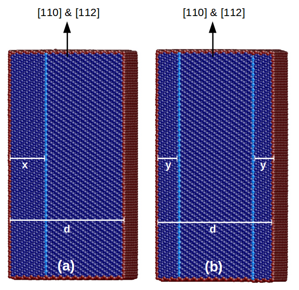
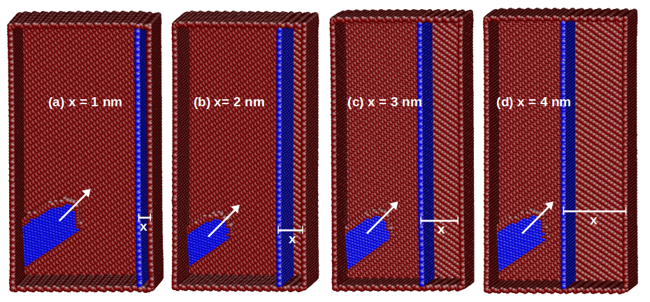
Twinned Cu nanopillars with an axial orientation of 110 and 112 direction have been considered in this study. The 110 nanopillar is enclosed by {111} and {112} type side surfaces, while the 112 nanopillar has {111} and {110} side surfaces. In these two nanopillars, one and two TBs have been introduced parallel to the nanopillar axis and their positions or distance (x and y) is varied with respect to nanopillar surface as shown in Figure 1a-b. In order to examine the size effects, twinned nanopillars with two different cross-section widths (d) = 10 and 15 nm have been investigated in this study. The nanopillar length (l) was twice the cross-section width (d). On these twinned nanopillars, the tensile loading has been simulated using molecular dynamics (MD) simulations. All MD simulations were carried out in LAMMPS package [23] employing an an embedded atom method (EAM) potential for Cu given by Mishin and co-workers [24]. This potential has been chosen for being able to reproduce stacking fault and twinning fault energies for Cu [25], which are key variables for predicting the dislocation nucleation and deformation mechanism related studies.
To mimic the geometry of nanopillars, no periodic boundary conditions were used in any direction during the simulations. Before applying tensile load, energy minimization was performed by conjugate gradient method to obtain a relaxed structure. To obtain the trajectory of atoms, velocity verlet algorithm was used to integrate the equations of motion with a time step of 2 fs. Following the energy minimization, the twinned nanopillars were equilibrated to required temperature of 10 K in a canonical ensemble (constant NVT) with a Nose-Hoover thermostat. Upon thermal equilibration, the deformation was carried out in a displacement-controlled manner at constant strain rate of s-1 by imposing displacements to atoms along the nanowire length that varied linearly from zero at the bottom fixed layer to a maximum value at the top fixed layer. The strain rate considered in this study is significantly higher than the experimental strain rates, nevertheless, it’s in the conventional range of usual MD simulations. The strain () was calculated as , where is instantaneous length and is the initial length of the nanowire. The stress was obtained using the Virial expression [26], which is equivalent to a Cauchy’s stress in an average sense. AtomEye package [27]and OVITO [28] have been used for the visualization of atomic snapshots with common neighbour analysis (CNA).
3 Results and Discussion
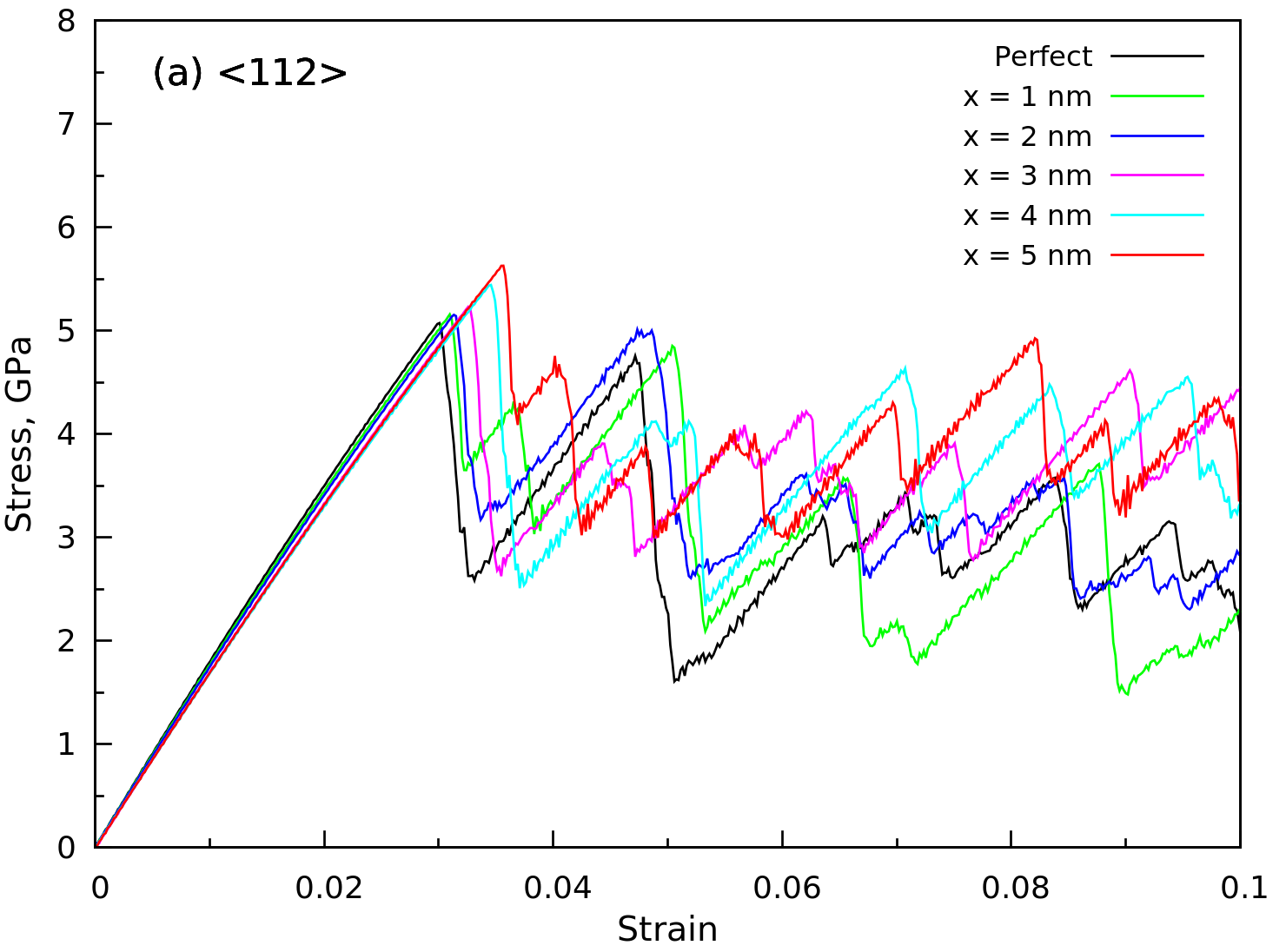
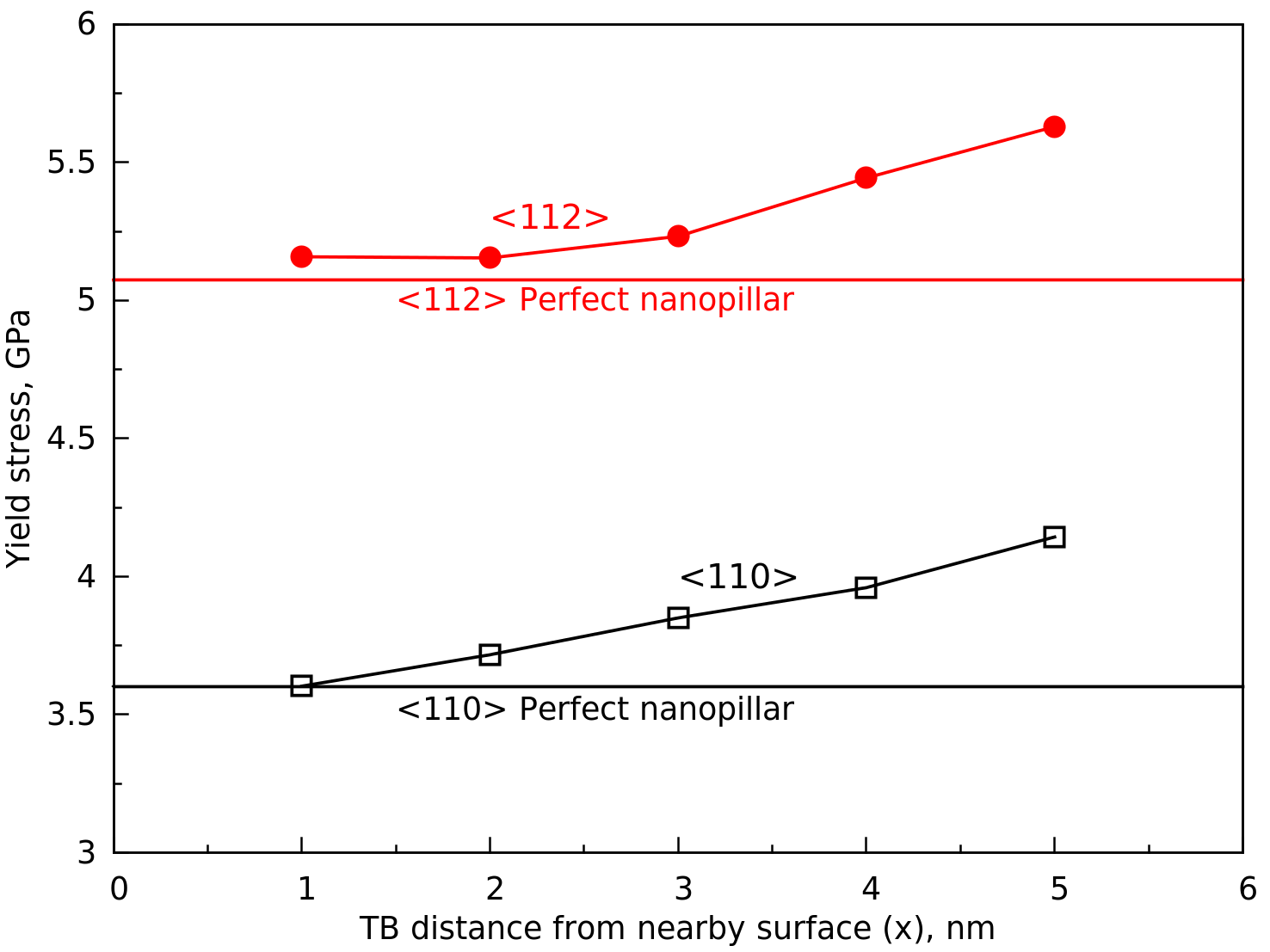
Figure 2(a)-(b) shows the tensile stress-strain behaviour of 112 and 110 oriented twinned Cu nanopillars containing a single axial TB located at various positions or distance (x) from the surface of the nanopillar with nm. It can be seen that both the nanopillars, irrespective of TB position, exhibit an initial linear elastic deformation till the peak value followed by a sudden drop in flow stress. This sudden drop indicates the commencement of plastic deformation in the nanopillars. With further increase in strain, the flow stress shows large fluctuations consisting of peaks and troughs, a typical signature of discrete plastic deformation in nanopillars[29]. Further in both the nanopillars (110 and 112), it can be seen that the TB position has no effect on the elastic deformation (Figure 2). However, the peak stress at the end of elastic deformation known as yield stress shows a significant and systematic variation with respect to TB position. Figure 3 depicts the variation of yield strength in 112 and 110 nanopillars as a function of TB distance (x) from the nearby pillar surface. For comparison, the yield strength of perfect nanopillars is also shown as horizontal line. It shows that in both the orientations, the yield strength increases with increasing the TB distance from the nanopillar surface (Figure 3). In other words, the strength is lowest when the TB is placed close to the surface and reaches maximum value when it is located at the center of the pillar (i.e., x = 5 nm), which is equal distance from both the surfaces. Further when the TB is close to surface (i.e., x = 1 nm), the strengthening effect of TB is negligible as the strength is almost comparable to the perfect nanopillar (Figure 3). Like twinned nanopillar with d = 10 nm, the yield strength of a nanopillar with d = 15 nm has also shown similar behaviour, however, the peak strength is observed at x = 7.5 nm. Finally in all the cases the strength of twinned nanopillars is always higher than the perfect nanopillar, as observed in previous investigations [19, 30].
In twinned nanopillars the increase in strength has been attributed to the repulsive force offered by the TBs on dislocation nucleation [16, 17, 18]. The repulsive force () exerted by the twin boundary on dislocations nucleating from a surface at a distance of is given by [16, 17, 18]
| (1) |
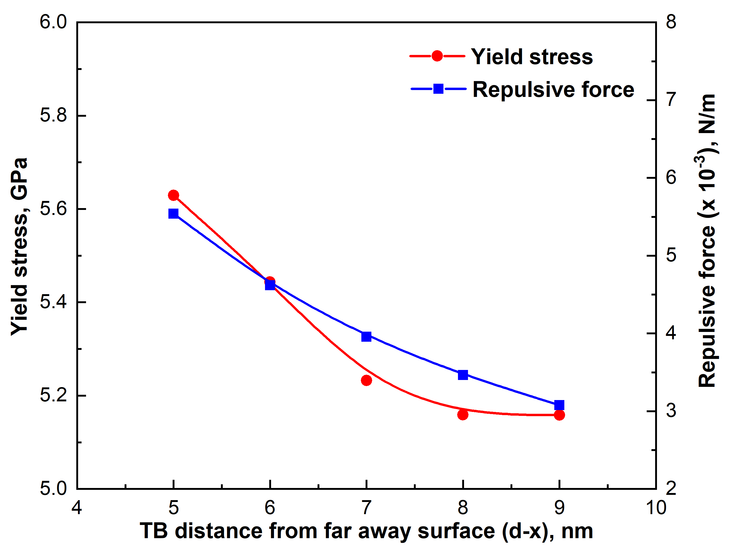
Here, is dimensionless measure of the interaction strength due to the elasticity mismatch between the twin and perfect crystal, is the shear modulus in the slip direction and b is the Burgers vector of partial dislocations. According to this equation, the strength should be maximum when the TB is close to nanopillar surface. However, the reverse behaviour is observed in Figure 3. In order to understand this peculiar behaviour, the atomic configurations of nanopillars during the yielding have been captured and analysed. Figure 4 shows the yielding in Cu nanopillar having a single TB at various distance from pillar surface. It can be seen that at all TB positions, the yielding occurs through the nucleation of 1/6112 Shockley partial dislocations from the nanopillar corners. Further, the nucleation occurs only in the larger grain, i.e, from corners that are far away from the TB (Figure 4). No nucleation of dislocations is observed in the smaller grain. As the Shockley partials nucleate from a surface which is far away from the TB, the distance between TB position and far away surface has to be considered in repulsive force calculations. In a nanopillar with single TB located at a distance of x nm from the nearby surface, the same boundary is located at a distance of “d-x” nm away from the far away surface, where d is the cross-section width of the nanopillar. Accordingly, the repulsive force equation has to be modified as follows;
| (2) |
Using this equation, the values of repulsive force have been calculated by substituting the appropriate values of , and . For Cu, = 0.3 [17] and = 53.31 GPa. The variations in repulsive force as a function of distance “d-x” is shown in Figure 5. For comparison, the yield stress values of 112 twinned nanopillar were also plotted with respect to “d-x”. It can be seen that, both yield stress and the repulsive force exhibit a similar decreasing behaviour with increasing distance “d-x” from the far away surface. Thus, there is clear correlation between the yield stress and the repulsive force on dislocations nucleating from the far away surface. This indicates that the distance between the TB and nanopillar surface dictate the strength of a nanopillar.
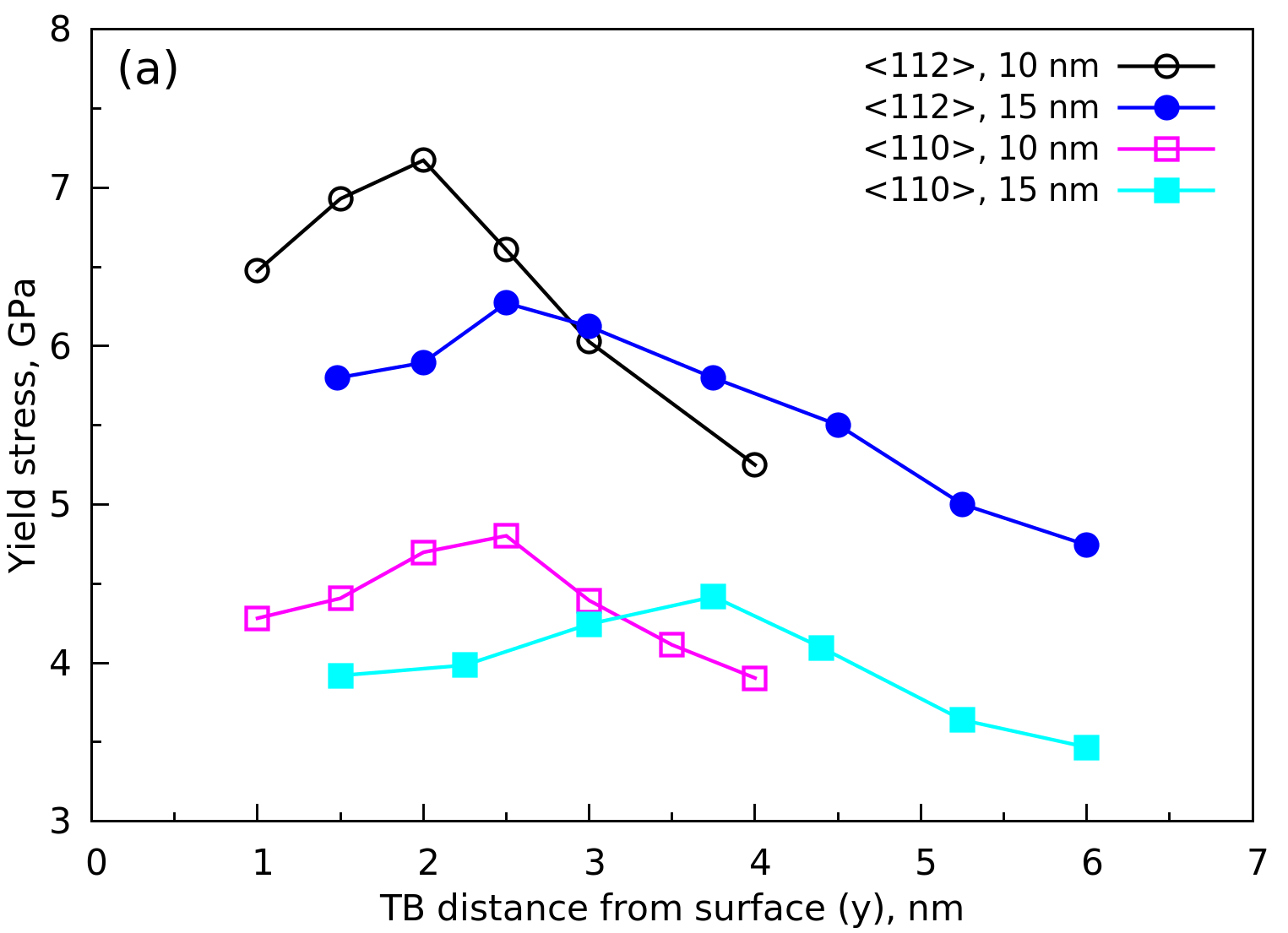
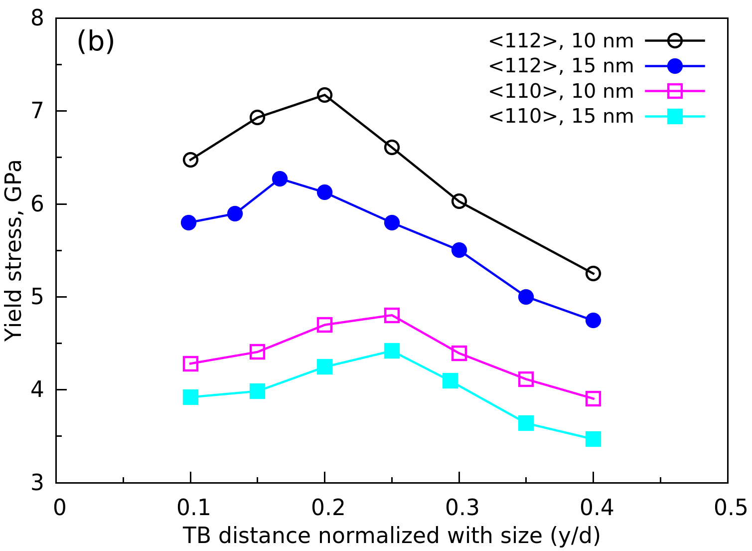
In addition to nanopillar containing a single TB, it is also interesting to examine the role of TB position when the nanopillar contains multiple TBs. For this, two TBs have been placed in the nanopillar, each at a distance of y from the surface (Figure 1b) and y is varied systematically. Figure 6a shows the tensile stress-strain behaviour of 112 Cu nanopillars with nm containing two TBs located at various positions or distance (y) from the surface. It can be seen that, overall the stress-strain behaviour is almost similar to that described for 112 nanopillar containing a single TB, which consist of an initial elastic deformation till the peak followed by a sudden drop in flow stress and then large fluctuations consisting of peaks and troughs during plastic deformation. However, as shown in Figure 6b, the yield stress of 112 nanopillar containing two TBs displayed a quit different behaviour as a function of TB position. At small distances from the pillar surface, the yield stress increases with increasing distance and reaches a maximum value at a distance of y = 2 nm followed by gradual decrease. Similar yield stress behaviour has been observed for nanopillar with different orientation (110) and size (Figure 7a-b). However, the important difference is the position of TB at which the nanopillar attains the peak strength. As can be seen in Figure 7a, for the same size (d = 10 nm), the peak strength in 110 nanopillars is observed at marginally higher value of y than that observed for 112 nanopillar. Similarly, for both 112 and 110 nanopillars, the position at which the nanopillars attains the peak strength increases with increasing size (Figure 7a). Specifically, in 110 nanopillars this position is found to be at y = 2.5 nm and 3.75 nm for the pillar sizes of 10 and 15 nm, respectively. For better understanding, the yield strength is plotted as a function of TB distance (y) normalized with nanopillar size (d) in Figure 7b. The results suggest that, irrespective of size, the strength is maximum in 110 nanopillars when the twin boundaries are placed at a y/d ratio of 0.25, i.e., at a distance of one fourth the nanopillar size from the surfaces. In 112 nanopillars, the strength is maximum for the y/d ratio of approximately 0.2 (Figure 7b), i.e., y should be one fifth the nanopillar size. Thus, irrespective of size and orientation, the TB position significantly influences the yield strength of twinned nanopillars.
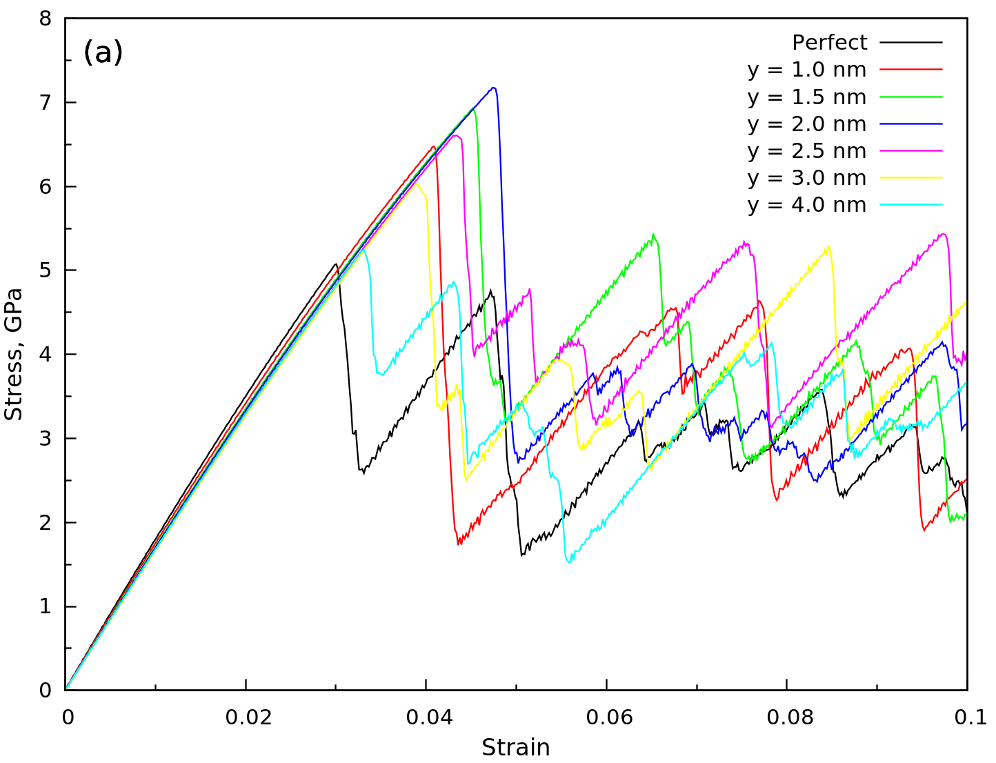
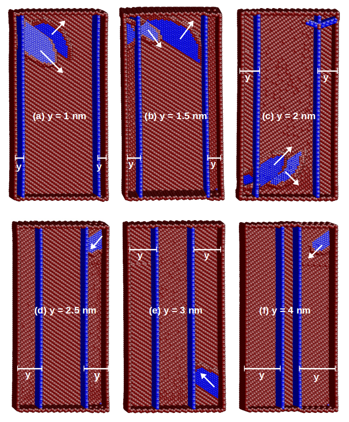
Unlike the nanopillar containing a single TB, the yield strength of the nanopillar containing two TBs shows a rather different behaviour (Figures 3 and 7). According to equation 1, the repulsive force should decrease with increasing suggesting that the yield strength should also show a decreasing trend with increasing twin boundary distance from the surface. However, this behaviour in yield strength is observed only at larger values of (Figure 7). At smaller values of , the yield strength increases with increasing the TB distance from the surface. In order to understand this anomalous behaviour, the defect nucleation during yielding has been carefully examined. Figure 8 shows the dislocation nucleation in 112 nanopillar containing two TBs located at various positions from the surface. It can be seen that, at small distances ( = 1,1.5 and 2 nm), the yielding occurs in the middle grain, which is also large in size (Figure 8a-c). Specifically, the dislocations nucleate from intersection of TB and surface. Contrary to this, the yielding at higher TB distances ( nm) occurs in the grains closer the surface (Figure 8d-f). Further in this case, no nucleation of dislocations is observed in the middle grain. In other words, there is a change in nucleation behaviour from middle grain to surface grains with increasing TB position from nanopillar surface. This change in dislocation nucleation behaviour is directly reflected in yield strength behaviour. At small distances where nucleation is observed in the middle grain, the repulsive force increases with increasing TB position as the TBs come closer to nucleation points, i.e., for small values of , the repulsive force is inversely proportional to the spacing between the twin boundaries (). On the contrary, at large TB distances, where nucleation is observed in the grains near to surface, the repulsive force decreases with increasing TB position as the TBs move away from nucleation points. This results in decrease of yield strength with increasing TB distance at large values of . It can be seen that in nanopillars with single and double TBs, the dislocation nucleation occurs mainly in the larger grains (Figures 4 and 8). This may be due to the availability of more volume (for dislocation glide) within the large grain, which decreases the activation energy for dislocation nucleation. As a result of this, Deng and Sansoz [17] have shown that the yield stress of twinned nanopillars depends only on the largest distance between the TB and dislocations, i.e., size of the largest grain where the dislocations nucleate. This phenomena is analogous to dislocation nucleation with respect to nanowire size, where dislocation nucleation is easier in large size nanowires compared to smaller ones [8].
It is well known that the nanopillar surfaces exerts an image force on dislocation nucleation, thus resulting in size dependent yield strength [31, 32]. The present results suggest that due to the repulsive force of TBs, the TB position from the nanopillar surface becomes an important factor in dictating the yield strength of twinned nanopillars. However, any kind of attractive/repulsive force between the TBs and surfaces, and TB-TB is not known, which needs future attention. Twin boundary position dependent yield strength as observed in the present study has great consequence in twinned nanocrysalline materials and also in materials where TB migration is extensively observed. In twinned polycrystalline Cu, Marchenko and Zhang [33] studied the effect of TB position on the mechanical properties by placing two TBs in each grain and varying their position with respect to the grain boundary [33]. Since the dislocations nucleate from grain boundaries (GBs), the distance between TB and GB played an important role on dislocation nucleation, strength and toughness. It has been reported that the strength and toughness values reach their maximum at an intermediate distance between TB and GB, while it decreases when they were far away or close to each other [33]. This variation of yield strength with respect to TB position in a polycrystalline material is similar to that observed in the present study, where yield strength varies with respect to TB position from the nanopillar surface. These results demonstrates that the mechanical properties of the twinned nanopillars or nanocrystalline materials can be controlled by carefully tailoring the position of the TBs within nanopillar/grain without changing their number density, unlike the case of TB spacing. The strengthening by tailoring the TB position has an advantage as compared to the strengthening by TB spacing. The strengthening by TB spacing requires the insertion of multiple TBs separated by an equal distance and small spacing requires high density of TBs. In contrast, the strengthening by TB position involves limited number of TBs (one or two) and only their position needs to be changed with respect to nanopillar surface/GB to get the desired strength. The present results may also suggest that in materials where TB migration is extensively observed [34], the change in the position of the TB with respect to the surface/GB may significantly influences the flow stress during the plastic deformation.
4 Conclusions
In the present study, the role of twin boundary (TB) position on dislocation nucleation and yield strength of twinned nanopillars has been investigated using MD simulations. The results indicated that the TB position or distance from the surface significantly influences the yield strength of twinned metallic nanopillars. Further, it has been observed that the effect of TB position is not always the same. When the nanopillar contains a single TB, the strength increases as the TBs move away from surface and attains the maximum when it is located at the center of the nanopillar. Further, in nanopillar containing single TB, the dislocations always nucleate from the surface which is far away from the TB. No nucleation of dislocations is observed from surface closer to the TB. Due to this, the repulsive force and correspondingly the yield strength increases with increasing TB distance x from the nearby surface (or decreasing TB distance from the far away surface, d-x). In case of a nanopillar containing two TBs, the yield strength initially increases with increasing TB distance and reaches a peak value before showing a gradually decreasing behaviour. In other words, there is an optimal distance (y) of TB at which the nanopillar containing two TBs exhibits a peak strength, which is found to be around one fourth and one fifth the nanopillar size for 110 and 112 orientations, respectively. In nanopillar containing two TBs, the dislocation nucleate in the middle grain when the TBs are close to surface (small y), while nucleation from the grains closer to surface has been observed when they are far away from the surface (large y). As a result, the yield strength is maximum at an intermediate distance between TBs and surface (y = d/4), while it decreases when the TBs are too close or too far from the surface. This study demonstrates that the mechanical properties of the twinned nanopillars can be controlled by carefully tailoring the position of the TBs within nanopillar without changing their number density.
Data availability
The data that support the findings in this paper are available from the corresponding author on request.
References
- [1] C.R. Weinberger, W. Cai, Plasticity of metal nanowires, J. Mater. Chem. 22 (2012) 3277-3292.
- [2] J.Wang, S.X. Mao, Atomistic perspective on in situ nanomechanics, Extr. Mech. Lett. 8 (2016) 127-139.
- [3] T. Zhu, J. Li, A. Samanta, A. Leach, K. Gall, Temperature and strain rate dependence of surface dislocation nucleation, Phys. Rev. Lett. 100 (2008) 025502.
- [4] B. Roos, B. Kapelle, G. Richter, C.A. Volkert, Surface dislocation nucleation controlled deformation of Au nanowires, Appl. Phys. Lett. 105 (2014) 201908.
- [5] A. Cao, E. Ma, Sample shape and temperature strongly influence the yield strength of metallic nanopillars, Acta Mater. 56 (2008) 4816-4828.
- [6] H. Xie, F. Yin, T. Yu, G. Lu, Y. Zhang, A new strain-rate-induced deformation mechanism of Cu nanowire: Transition from dislocation nucleation to phase transformation, Acta Mater. 85 (2015) 191-198.
- [7] P. Rohith, G. Sainath, B.K. Choudhary, Effect of orientation and mode of loading on deformation behaviour of Cu nanowires, Comp. Condens. Mat. 17 (2018) e00330.
- [8] G. Sainath, P. Rohith, B.K Choudhary, Size dependent deformation behaviour and dislocation mechanisms in 100 Cu nanowires, Philos. Mag. 97 (2017) 2632-2657.
- [9] A.J. Cao, Y.G. Wei, S.X. Mao, Deformation mechanisms of face-centered-cubic metal nanowires with twin boundaries, Appl. Phys. Lett. 90 (2007) 151909.
- [10] K.A. Afanasyev, F. Sansoz, Strengthening in gold nanopillars with nanoscale twins, Nano Lett. 7 (2007) 2056-2062.
- [11] L. Lu, X. Chen, Revealing the maximum strength in nanotwinned copper, Science 323 (2009) 607-610.
- [12] D. Jang, X. Li, H. Gao, J.R. Greer, Deformation mechanisms in nanotwinned metal nanopillars, Nat. Nanotechnol. 7 (2012) 594-601.
- [13] P. Rohith, G. Sainath, Sunil Goyal, A. Nagesha, V.S. Srinivasan, Role of axial twin boundaries on deformation mechanisms in Cu nanopillars, Philos. Mag. 100 (2019) 529-550.
- [14] Z. Yang, L. Zheng, Y. Yue, Z. Lu, Effects of twin orientation and spacing on the mechanical properties of Cu nanowires, Sci. Rep. 7 (2017) 10056.
- [15] G. Sainath, B.K. Choudhary, Deformation behaviour of body centered cubic iron nanopillars containing coherent twin boundaries, Philos. Magaz. 96 (2016) 3502-3523.
- [16] Z. Chen, Z. Jin, and H. Gao, Repulsive force between screw dislocation and coherent twin boundary in aluminum and copper, Phys. Rev. B 75 (2007) 212104.
- [17] C. Deng, F. Sansoz, Repulsive force of twin boundary on curved dislocations and its role on the yielding of twinned nanowires, Scr. Mater. 63 (2010) 50-53.
- [18] X. Guo and Y. Xia, Repulsive force vs. source number: Competing mechanisms in the yield of twinned gold nanowires of finite length, Acta Mater. 59 (2011) 2350-2357.
- [19] G. Sainath, B.K. Choudhary, Molecular dynamics simulation of twin boundary effect on deformation of Cu nanopillars, Phys. Lett. A 379 (2015) 1902-1905.
- [20] G. Cheng, S. Yin, T.-H. Chang, G. Richter, H. Gao, and Y. Zhu, Anomalous tensile de-twinning in twinned nanowires, Phys. Rev. Lett. 119 (2017), p. 256101.
- [21] W.S. Ko, A. Stukowski, R. Hadian, A. Nematollahi, J.B. Jeon, W.S. Choi, G. Dehm, J. Neugebauer, C. Kirchlechner, B. Grabowski, Atomistic deformation behavior of single and twin crystalline Cu nanopillars with preexisting dislocations, Acta Mater. 197 (2020) 54-68.
- [22] J.B. Jeon, G. Dehm, Formation of dislocation networks in a coherent Cu twin boundary, Scr. Mater. 102 (2015) 71-74.
- [23] S. Plimpton, Fast parallel algorithms for short-range molecular dynamics, J. Comp. Phy. 117 (1995) 1-19.
- [24] Y.Mishin, M.J. Mehl, D.A. Papaconstantopoulos, A.F. Voter, J.D. Kress, Structural stability and lattice defects in copper: Ab initio, tight-binding, and embedded-atom calculations, Phys. Rev. B, 63 (2001) 1-16.
- [25] W. Liang, M. Zhou, Atomistic simulations reveal shape memory of fcc metal nanowires, Phys. Rev. B 73 (2006) 115409.
- [26] J.A. Zimmerman, E.B. Webb, J.J. Hoyt, R.E. Jones, P.A. Klein, D.J. Bammann, Calculation of stress in atomistic simulations, Modell. Simul. Mater. Sci. Eng. 12 (2003) S319-s332.
- [27] J. Li, AtomEye: an efficient atomistic configuration viewer, Modell. Simul. Mater. Sci. Eng. 11 (2003) 173-177.
- [28] A. Stukowski, Visualization and analysis of atomistic simulation data with OVITO-the Open Visualization Tool, Modell. Simul. Mater. Sci. Eng. 18 (2010) 015012.
- [29] H. Zheng, A. Cao, C.R. Weinberger, J.Y. Huang, K. Du, J. Wang, Y. Ma, Y. Xia and S.X. Mao, Discrete plasticity in sub-10-nm-sized gold crystals, Nat Commun. 1 (2010) 144.
- [30] C. Deng, F. Sansoz, Size-dependent yield stress in twinned gold nanowires mediated by site-specific surface dislocation emission, Appl. Phys. Lett. 95 (2009) 091914.
- [31] W. Ye, A. Ougazzaden, M. Cherkaoui, Analytical formulations of image forces on dislocations with surface stress in nanowires and nanorods, Inter. J. Solids and Struct. 50 (2013) 4341-4348.
- [32] Q.-J. Li, B. Xu, S. Hara, J. Li, E. Ma, Sample size-dependent surface dislocation nucleation in nanoscale crystals, Acta Mater. 145 (2018) 19-29.
- [33] A. Marchenko, H. Zhang, Effects of location of twin boundaries and grain size on plastic deformation of nanocrystalline copper, Metall. and Mat. Trans. A 43A (2012) 3547-3555.
- [34] Y.B. Wang, M.L. Sui, and E. Ma, In situ observation of twin boundary migration in copper with nanoscale twins during tensile deformation, Phil. Mag. Lett. 87 (2007) 935-942.