An Open-Source RRAM Compiler
Abstract
Memory compilers are necessary tools to boost the design procedure of digital circuits. However, only a few are available to academia. Resistive Random Access Memory (RRAM) is characterised by high density, high speed, non volatility and is a potential candidate of future digital memories. To the best of the authors’ knowledge, this paper presents the first open source RRAM compiler for automatic memory generation including its peripheral circuits, verification and timing characterisation. The RRAM compiler is written with Cadence SKILL programming language and is integrated in Cadence environment. The layout verification procedure takes place in Siemens Mentor Calibre tool. The technology used by the compiler is TSMC 180nm. This paper analyses the novel results of a plethora of M x N RRAMs generated by the compiler, up to M = 128, N = 64 and word size B = 16 bits, for clock frequency equal to 12.5 MHz. Finally, the compiler achieves density of up to 0.024 Mb/mm2.
I Introduction
The progress of the technology has lead to an aggressive scaling trend of Integrated Circuits (IC), generating great demand for high density, high speed and low power memories [1]. However, customised memory design is a resource-intensive task [2, 3, 4]. Therefore, a number of memory compilers has been presented before [4, 2, 3, 5, 6, 7]. These compilers mainly focus on two types of memories, the volatile memories (e.g. static or dynamic random access memory) and the non volatile memories (e.g. flash memory) [8, 9]. Volatile memories suffer of high power consumption and loss of data on power off, while non volatile memories require high write voltage and suffer of low endurance and low speed [9, 10].
A novel emerging non volatile memory which is characterised by scalability, high speed, high density and low power is the Resistive Random Access Memory (RRAM). RRAM uses memristors in its memory cells [11, 8, 10, 12, 9, 13, 14]. Therefore, a RRAM compiler is an essential tool to boost the RRAM design procedure and facilitate the research of the memristive device properties [15].
The work presented in [15] described a novel RRAM architecture and demonstrated the results only of the RRAM array generation and its layout verification. This paper extends this work by improving the RRAM architecture described in [15] and presents the first open source RRAM compiler which automatically generates the RRAM including its peripheral circuits, verifies their layout and performs timing characterisation. The features of the RRAM compiler presented in this work are presented in Tab. I. It is clear that the work presented in [15] includes partially only two features of the RRAM compiler presented in this paper. The proposed RRAM compiler includes new features regarding Place and Route (P&R) of memory blocks, co-integration of analogue and digital blocks, layout verification of the whole RRAM and timing characterisation. The source code of the proposed RRAM compiler has been published on Github:
This Section briefly described the background regarding RRAMs, memory compilers and the new features of the proposed RRAM compiler. Section II presents the RRAM architecture and its most important blocks. In Section III the RRAM compiler structure and the characterisation procedure are described. Section IV analyses the results produced by a number of automatically generated designs. Finally, Section V summarises this paper.
| Architecture | Functionalities | Work [15] | This Work |
| RRAM array | RRAM array generation | Yes | Yes |
| Peripheral analogue circuits | Reference cells generation | No | Yes |
| Multiplexers generation | No | Yes | |
| Write Amplifiers generation | No | Yes | |
| Analogue P&R | No | Yes | |
| Analogue co-integration | No | Yes | |
| Peripheral digital circuits | Synthesis | No | Yes |
| Implementation | No | Yes | |
| Design constraints generation | No | Yes | |
| GDS and Verilog import | No | Yes | |
| System-level | Mixed-signal P&R | No | Yes |
| Mixed-signal co-integration | No | Yes | |
| Layout generation | No | Yes | |
| Layout verification | Yes | Yes | |
| System characterisation | No | Yes |
II RRAM Architecture
II-A RRAM Architecture Overview
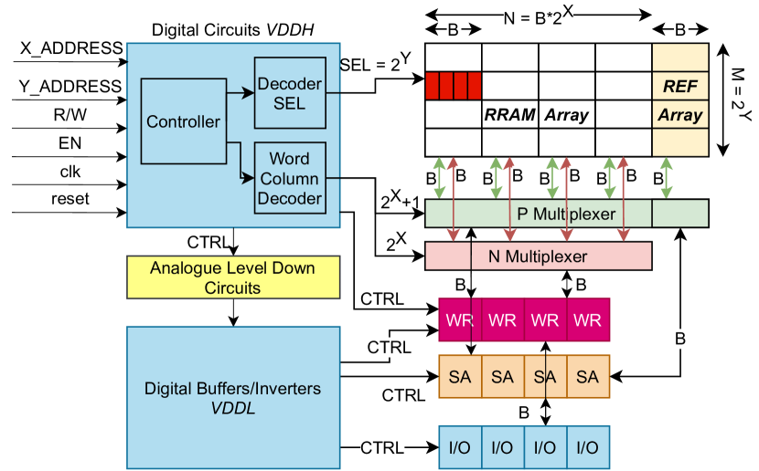
A simplified block diagram of the proposed RRAM architecture is shown in Fig. 1. The size of the RRAM array is M N, where M = 2Y and N = B2X. A word of B memory cells is shown under red colour. Blue blocks represent digital circuits, while the rest of them represent analogue circuits. Compared to the architecture presented in [15], reference cells array, B additional of P multiplexer switches and level-shifters between digital blocks have been introduced.
A multiplexer switch consists of a grounding NMOS and a transmission gate. The P multiplexer has one more block of B switches compared to the N multiplexer due to the fact that it connects the reference cells array to the sense amplifiers.
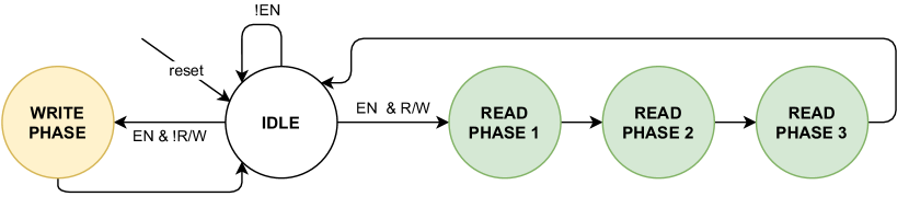
Six signals are needed to control the RRAM in contrast with [15], where only the three very basic were introduced. These are the X_ADDRESS[X:1] signal (address of the desired word column), the Y_ADDRESS[Y:1] signal (address of the desired row), the EN signal (enable chip), the R/W signal (read or write operation), the clock of the chip and the reset signal. The desired word to be read or written is interfaced through I/O ports. A simplified Finite State Machine (FSM) of the digital controller is depicted in Fig. 4.
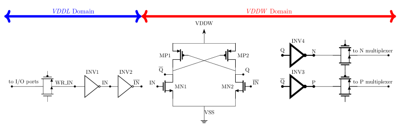
RRAM uses three power supplies. Memory cells have been designed with high voltage (VDDH) technology transistors. Therefore, a number of digital circuits, P and N multiplexer also operate under VDDH voltage. On the other hand sense amplifiers, have to ensure that the voltage applied on the bitlines does not alter the state of the memristor of the memory cells, thus VDDL has been chosen for the sense amplifiers [15]. The sense amplifier incorporates low voltage (VDDL) technology transistors. The digital signals that control (CTRL) VDDL circuits have to be levelled down through an analogue level-shifter circuit and they are propagated to the sense amplifiers array and I/O ports through digital buffers or inverters. In order to provide flexibility on the write voltage, a third power supply VDDW has also been included in the design.
The reference cell consists of a NMOS transistor. The drain source resistance of the transistor represents the reference resistance RREF. Its resistance is compared against the corresponding memory cell resistance, when it is sensed by the corresponding sense amplifier. The reference cells are integrated alongside the RRAM array, as they share same lines and have same layout size. The size of the reference cells array is M B.
II-B Write Circuit
The write voltage (VDDW) differs based on the memristor materials. The write circuit is shown in Fig. 2. The devices in Figures with thick line make use of transistor models able to support up to VDDH voltage, while the others are able to support up to VDDL respectively. WR_IN can be 0 V or VDDL. Transistors MN1, MN2, MP1, MP2 and INV2 form a conventional level-shifter with positive feedback[16]. Thus, if WR_IN is digital 0, which is modelled in this implementation as Low Resistance State (LRS), then Q will go high, as such, P will be VDDW and N will be 0 V. On the contrary, if WR_IN is digital 1 or VDDL, which is modelled in this implementation as High Resistance State (HRS), then P will be 0 V and N will be VDDW. These values will be propagated to the desired memory cell through the P and N multiplexers.
II-C Sense Amplifier
The sense amplifier is based on those presented in [17, 18] and it is shown in Fig. 3. Transistors M2, M5, M3, M6 form a typical cross coupled inverters sense amplifier. Transistors M1 and M4 precharge VO1, VO2 to VDD. In this case VDD refers to VDDL. A common gate configuration is used for the input stage, keeping the input impedance (M9 and M10 source terminal) as low as possible. Transistors M9 and M10 operate in triode region and they force a low voltage on bitlines VBL, VBLB. Transistor M8 is an equaliser that ensures that equal values are set on VO1 and VO2. Three additional transistors forming a transmission gate and a grounding NMOS, enable the sense of the memory cell when read operation is executed. Further to this, there is also a transmission gate that connects VO1 to I/O ports.

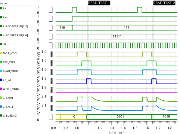
The sense amplifier operates in three phases. Its operation is illustrated in Fig. 6. When READ signal is high, phase 1 starts. Signal PRE remains low, DVLP goes high and current is drawn from the memory cell and the reference cell. In phase 2, PRE goes high, therefore, VO1 and VO2 are no longer equal and the voltage difference, which is developed between them, is rapidly enhanced. In phase 3, DVLP goes low and EN (or EN_SA) goes high, forcing the result to rail to rail output voltage value. In Fig. 6, vertical lines READ TEST 1 and READ TEST 2 show the moment where EN_SA is set to high and the output of the first (Z_SA[0]) and the second (Z_SA[1]) sense amplifier has been propagated to the bus (Z_BUS[3:0]) of the tri state buffers (I/O ports).
III RRAM compiler
The RRAM compiler is written in SKILL language and is invoked by Command Interpreter Window (CIW) of Cadence Virtuoso 6.1.8 [19, 20]. The very basic arguments are the dimensions (M, N, B) of the memory. Further optional arguments, such as the minimum clock frequency can be specified. The RRAM compiler procedure follows the features presented from top to bottom in Tab. I. The RRAM compiler makes use of Cadence Virtuoso for analogue design and Cadence Genus and Innnovus for digital design [21, 22, 23, 24, 25, 26]. It also verifies the layout correctness of the generated RRAMs by executing Design Rule Checking (DRC) and Layout Versus Schematic (LVS) tests in Mentor Calibre tool [27, 28]. The post-layout view of the RRAM generated by Parasitic Extraction (PEX) tool of Mentor Calibre is used in the timing characterisation procedure. The timing characterisation procedure is invoked by an automatically generated OCEAN script [29]. An example of an automatically generated layout by the RRAM compiler is shown in Fig. 5.
The RRAM characterisation procedure generates a testbench which includes the RRAM block and a verilog block with test signals. The post-layout view of the analogue part of the RRAM and the P&R verilog netlist of the digital circuits are used by the mixed signal simulator in Cadence Virtuoso. The automatically generated RRAMs are tested for Typical Typical (TT), Fast Slow (FS), Slow Fast (SF), Slow Slow (SS) and Fast Fast (FF) NMOS and PMOS models at nominal corner. During the simulation, the Standard Delay Format (SDF) files produced by Innovus after P&R are used to provide realistic results for the digital circuits. The testbench performs initially a reset and then two extreme conditions write (W1, W2) and two read (R1, R2) tests.
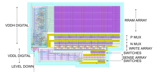
By inspection of Fig. 5, it is clear that the worst case read/write operation occurs for the words that are located at the top right corner of the layout, where is the furthest distance from the read/write circuits. Therefore, the loading time of the lines involved in read/write operation for these cells will be the greatest. In the first write test (W1), the word is located at position X_ADDRESS = 2X-1 and Y_ADDRESS = 2Y. This word is the second to the last word on the top row of the RRAM array. The LRS and HRS values depend on the material characteristics. It is well known that a number of memristors get resistance values in the range of a few Ohms to tens of kOhms [14, 30]. Given that, the memristance of the memory cells is emulated with a resistance equal to 1 MΩ as an extreme value to examine worst case settling time across the memory cell. The desired value to be written on this test is 10…10, resulting in VPN (Voltage across P and N terminal of memory cell) being positive for a 0, and negative for a 1. The voltage across P and N terminals of the word is checked at 0.4 clock time later than the write phase has started by the controller. This is because the clock waveform that is used by the synthesis has 50% duty cycle. Therefore, this value has to be set up in time. The test checks whether, at this point of time, the desired VPN is greater than 0.7 VDDW when I/O = 0 or VPN is less than -0.7 VDDW when I/O = 1. As a default value, VDDW is set by the compiler to 3.3 V. Memristors write voltage can vary from around 2 V to up to 10 V or more [14]. The limit 0.7 VDDW is a demonstration limit and should be set according to the device characteristics. The W2 test performs the same checks. The only difference is that the desired value to be written is the complementary one 01…01 compared to the previous test.
Similarly, two tests are executed to verify correctness of the read operation. In read tests, the last word of the top row is selected. The address of this word is X_ADDRESS = 2X and Y_ADDRESS = 2Y. In this case, the memristance of each memory cell is also emulated with a resistor (representing extreme HRS and LRS values). In the first read (R1) test, the resistances of the cells of the word under test are initialised with respect to a value . By default is set equal to 0.3. Then, LRS is equal to RREF and HRS is equal to RREF. In this case, RREF was set equal to 32.5 kΩ as a typical median resistance value of a memristor. In the first read test (R1), the word is initialised to value LRS, HRS…LRS, HRS. Therefore, for HRS, logical 1 should be read at the output 1 and for LRS, logical 0 respectively. Same as previously, the check takes place 0.4 clock time later than the third phase of the read procedure, as the read value has to be set up in time for the tri state buffers to hold it. In this case, regarding the cells that have been initialised with the HRS value, it is checked whether the value at the output of the sense amplifier is greater than 0.83 VDDL. For those which have been initialised with the LRS value, it is checked if the value at the output of the sense amplifier is less than 0.16 VDDL. The second read test is the same as above. The only difference is that the complementary value HRS, LRS…HRS, LRS is set on the word under test. An example of the R1, R2 tests for the first two bits of the word under test in the memory is shown in Fig. 6.
IV Results
Multiple sizes were tested, as it is shown on Tab. II. Maximum clock frequency was set to 25 MHz, as this is the maximum clock frequency that meets the digital synthesis design constraints. A table with the results for 12.5 MHz is shown on Tab. II. Memories succeed in all write tests, while some of them fail to pass the read tests mainly for FS and FF corners. This occurs due to the fact that only one output of the sense amplifiers is used in this topology. This output is connected to a bus while the other one is floating, as such, there is an imbalance between the driving output load. The author suggests that the sense amplifiers should be isolated by connecting their input/outptus to buffers. Write operations are correct (all corners) for an up to 8 kb memory and write time 80 ns. Write test, in greater frequencies, may fail due to the big loading time on the terminals of the memory cells. Additionally, read operations are correct (all corners) for an up to 8 kbit memory with B = 4 and access time approximately equal to 2/3 clock, which is 160 ns. Fastest access time is equal to 80 ns and it is achieved for an up to 1 kbit memory with B = 4 and clock frequency 25 MHz. The best density (RRAM bit size / RRAM layout size) achieved by the compiler is 0.024 Mb/mm2 in TSMC 180 nm technology.
Furthermore, by using three power supplies the design becomes less robust and complex. The author suggests that the architecture could be redesigned and simplified by using only one power supply VDDH. The write circuit could be replaced with a programmable digital to analogue converter (DAC) to provide the necessary flexibility on the write voltage. Finally, the reference array could be potentially replaced by a programmable current mirror.
Memristance is a property that arises particularly in thin film devices, which are extremely small in size. The current implementation takes into account their size by placing corresponding pins on the top metals of RRAM cells. In this way, memristors can be placed on top of the RRAM array after the CMOS fabrication of the memory. However, the RRAM compiler uses ideal resistors for their emulation in the timing characterisation procedure. As a future improvement, the authors suggest the use of a realistic model of a memristor in order to account for even more realistic results. Additionally, temperature variation should be included in the tests. Furthermore, the power estimation of the RRAM should be introduced in future versions of the RRAM compiler.
| N | M | B | Nominal | FS | SF | SS | FF | report |
| 32 | 32 | 4 | pass | pass | pass | pass | pass | link |
| 64 | 16 | 4 | pass | pass | pass | pass | pass | link |
| 64 | 16 | 8 | fail (R1) | fail (R1, R2) | pass | pass | fail (R1, R2) | link |
| 64 | 32 | 4 | pass | pass | pass | pass | pass | link |
| 64 | 32 | 8 | fail (R1, R2) | fail (R1, R2) | pass | pass | fail (R1, R2) | link |
| 64 | 64 | 4 | pass | pass | pass | pass | pass | link |
| 64 | 64 | 8 | pass | fail (R1, R2) | pass | near | fail (R1, R2) | link |
| 128 | 16 | 4 | pass | pass | pass | pass | pass | link |
| 128 | 16 | 8 | pass | fail (R1, R2) | pass | pass | fail (R1, R2) | link |
| 128 | 16 | 16 | fail (R1, R2) | fail (R1, R2) | fail (R1, R2) | fail (R1, R2) | fail (R1, R2) | link |
| 128 | 32 | 4 | pass | pass | pass | pass | pass | link |
| 128 | 32 | 8 | pass | fail (R1, R2) | pass | pass | fail (R1, R2) | link |
| 128 | 32 | 16 | fail (R1, R2) | fail (R1, R2) | fail (R1, R2) | fail (R1, R2) | fail (R1, R2) | link |
| 128 | 64 | 4 | pass | pass | pass | pass | pass | link |
| 128 | 64 | 8 | pass | fail (R1, R2) | pass | pass | fail (R1, R2) | link |
| 128 | 64 | 16 | fail (R1, R2) | fail (R1, R2) | fail (R1, R2) | fail (R1, R2) | fail (R1, R2) | link |
A direct comparison between RRAMs cannot be made as they refer to different sizes and different materials. A density comparison between volatile memories, this work and the RRAM sub-arrays generated by the corresponding RRAM compilers presented in [34] and [15] is shown on Tab. III. RRAM compilers generate quite dense designs similar to SRAM designs. This work achieves approximately same density with an SRAM designed at TSMC 180 nm technology. The memory cell of the proposed implementation is relatively big to ensure robustness and low mismatch. It can be further reduced to improve the density. The optimal size of the RRAM cell should be further investigated. Fully custom made RRAMs exploiting multi state bit memory cells can achieve up to 6.66 Mb/mm2 and read/write access time less than 200 ns for up to 4 Mb designs [36, 37, 38]. The RRAM compiler presented in [39] exploits 3D IC design to further improve density, however the results are normalised and a direct comparison cannot be made.
V Conclusion
Taking everything into consideration, this paper presented the first open source RRAM compiler which automatically generates the RRAM array, the peripheral circuits and provides layout verification and timing characterisation. In this way, a number of memristors can be integrated and tested by using the automatically generated designs. Finally, the RRAM compiler serves as a great tool for both industry and academia in order to boost the RRAM design procedures and the investigation of the RRAM properties.
Acknowledgment
The authors acknowledge the support of the EPSRC FORTE Programme Grant (EP/R024642/1).
References
- [1] Y. Chen, “ReRAM: History, status, and future,” IEEE Transactions on Electron Devices, vol. 67, no. 4, pp. 1420–1433, 2020, [Online].
- [2] Y. Xu et al., “A flexible embedded SRAM IP compiler,” in 2007 IEEE ISCAS. IEEE, 2007, pp. 3756–3759, [Online].
- [3] M. R. Guthaus et al., “Openram: An open-source memory compiler,” in 2016 IEEE/ACM ICCAD. IEEE, 2016, pp. 1–6, [Online].
- [4] T. Shah et al., “FabMem: A multiported RAM and CAM compiler for superscalar design space exploration.” 2010, [Online].
- [5] S. Wu et al., “A 65nm embedded low power SRAM compiler,” in 13th IEEE Symposium on DDECS. IEEE, 2010, pp. 123–124, [Online].
- [6] R. Goldman et al., “Synopsys’ educational generic memory compiler,” in 10th EWME. IEEE, 2014, pp. 89–92, [Online].
- [7] M. Clinton et al., “A 5GHz 7nm L1 cache memory compiler for high-speed computing and mobile applications,” in 2018 IEEE ISSCC. IEEE, 2018, pp. 200–201, [Online].
- [8] A. Chen, “A review of emerging non-volatile memory (NVM) technologies and applications,” Solid-State Electronics, vol. 125, pp. 25–38, 2016, [Online].
- [9] F. Zahoor et al., “Resistive random access memory (RRAM): an overview of materials, switching mechanism, performance, multilevel cell (MLC) storage, modeling, and applications,” Nanoscale research letters, vol. 15, no. 1, pp. 1–26, 2020, [Online].
- [10] S. Maheshwari et al., “Hybrid CMOS/memristor circuit design methodology,” arXiv preprint arXiv:2012.02267, 2021, [Online].
- [11] D. B. Strukov et al., “The missing memristor found,” nature, vol. 453, no. 7191, pp. 80–83, 2008, [Online].
- [12] J. J. Yang et al., “Memristive devices for computing,” Nature nanotechnology, vol. 8, no. 1, pp. 13–24, 2013, [Online].
- [13] D. Ielmini et al., “In-memory computing with resistive switching devices,” Nature Electronics, vol. 1, no. 6, pp. 333–343, 2018, [Online].
- [14] S. Stathopoulos et al., “An electrical characterisation methodology for benchmarking memristive device technologies,” Scientific reports, vol. 9, no. 1, pp. 1–10, 2019, [Online].
- [15] D. Antoniadis et al., “Open-source memory compiler for automatic RRAM generation and verification,” in 2021 IEEE MWSCAS, 2021, pp. 97–100, [Online].
- [16] D. Dwivedi et al., “Voltage up level shifter with improved performance and reduced power,” in 2012 25th IEEE Canadian Conference on Electrical and Computer Engineering (CCECE), 2012, pp. 1–4, [Online].
- [17] I. P. Tolić et al., “Design of sense amplifiers for non-volatile memory,” in 2019 42nd International Convention on Information and Communication Technology, Electronics and Microelectronics (MIPRO). IEEE, 2019, pp. 59–64, [Online].
- [18] M. Suma et al., “Analysis of sense amplifier circuits in nanometer technologies,” in 2017 Fourth International Conference on Signal Processing, Communication and Networking (ICSCN). IEEE, 2017, pp. 1–4, [Online].
- [19] Cadence SKILL Language Reference Product Version ICADVM20.1, Cadence Design Systems, San Jose, USA, 2021.
- [20] Cadence SKILL Language User Guide Product Version ICADVM20.1, Cadence Design Systems, San Jose, USA, 2021.
- [21] Virtuoso Analog Design Environment XL User Guide Product Version IC6.1.8, Cadence Design Systems, San Jose, USA, 2021.
- [22] Virtuoso Layout Suite XL User Guide Product Version IC6.1.8, Cadence Design Systems, San Jose, USA, 2021.
- [23] Virtuoso Schematic Editor User Guide Product Version ICADVM20.1, Cadence Design Systems, San Jose, USA, 2021.
- [24] Virtuoso ADE Explorer User Guide Product Version ICADVM20.1, Cadence Design Systems, San Jose, USA, 2021.
- [25] Genus User Guide 20.1 Product Version 20.1, Cadence Design Systems, San Jose, USA, 2020.
- [26] Innovus User Guide Product Version 21.10, Cadence Design Systems, San Jose, USA, 2021.
- [27] Calibre® Interactive™ (New GUI) User’s Manual, Siemens Mentor, 2020.
- [28] Calibre® Verification User’s Manual, Siemens Mentor, 2020.
- [29] OCEAN Reference Product Version ICADVM20.1, Cadence Design Systems, San Jose, USA, 2021.
- [30] K. Nikiruy et al., “A precise algorithm of memristor switching to a state with preset resistance,” Technical Physics Letters, vol. 44, no. 5, pp. 416–419, 2018, [Online].
- [31] S. Miyano et al., “Highly energy-efficient SRAM with hierarchical bit line charge-sharing method using non-selected bit line charges,” IEEE JSSC, vol. 48, no. 4, pp. 924–931, 2013, [Online].
- [32] S. O. Toh et al., “Characterization of dynamic SRAM stability in 45 nm CMOS,” IEEE JSSC, vol. 46, no. 11, pp. 2702–2712, 2011, [Online].
- [33] K. Kushida et al., “A 0.7 V single-supply SRAM with 0.495 m2 cell in 65 nm technology utilizing self-write-back sense amplifier and cascaded bit line scheme,” IEEE JSSC, vol. 44, no. 4, pp. 1192–1198, 2009, [Online].
- [34] E. Lee et al., “A ReRAM memory compiler with layout-precise performance evaluation,” in 2019 IEEE SOI-3D-Subthreshold Microelectronics Technology Unified Conference (S3S). IEEE, 2019, pp. 1–3, [Online].
- [35] C. A. Kumar et al., “Performance analysis of low power 6T SRAM cell in 180nm and 90nm,” in 2016 2nd International Conference on AEEICB, 2016, pp. 351–357, [Online].
- [36] S.-S. Sheu et al., “A 4Mb embedded SLC resistive-RAM macro with 7.2ns read-write random-access time and 160ns MLC-access capability,” in 2011 IEEE International Solid-State Circuits Conference, 2011, pp. 200–202, [Online].
- [37] S.-S. Sheu et al., “Fast-write Resistive RAM (RRAM) for embedded applications,” IEEE Design Test of Computers, vol. 28, no. 1, pp. 64–71, 2011, [Online].
- [38] M. Zangeneh et al., “Design and optimization of nonvolatile multibit 1T1R Resistive RAM,” IEEE Transactions on Very Large Scale Integration (VLSI) Systems, vol. 22, no. 8, pp. 1815–1828, 2014, [Online].
- [39] E. Lee et al., “A ReRAM memory compiler for monolithic 3D integrated circuits in a carbon nanotube process,” ACM Journal on Emerging Technologies in Computing Systems (JETC), vol. 18, no. 1, pp. 1–20, 2021, [Online].