Real time phase imaging with an asymmetric transfer function metasurface
Abstract
The conversion of phase variations in an optical wavefield into intensity information is of fundamental importance for optical imaging technology including microscopy of biological cells. While conventional approaches to phase-imaging commonly rely on bulky optical components or computational post processing, meta-optical devices have recently demonstrated all-optical, ultracompact image processing methods. Here we describe a metasurface that exploits photonic spin-orbit coupling to create an asymmetric optical transfer function for real time phase-imaging. The effect of the asymmetry on transmission through the device is demonstrated experimentally with the generation of high contrast pseudo-3D intensity images of phase variations in an optical wavefield without the need for post-processing. This non-interferometric method has potential applications in biological live cell imaging and real-time wavefront sensing.
While the intensity of an optical field is readily measured with conventional camera technology, some applications require information beyond the intensity, such as polarization and phase. Phase-imaging is fundamental to imaging live, unstained biological cells and permits the investigation of cell dynamics and the detection of disease Park et al. (2018). Conventional all-optical, phase-imaging methods, including differential interference contrast (DIC) Arnison et al. (2004), Zernike phase-contrast microscopy Zernike (1942) and other interference-based approaches, require bulk-optical components and light progragation over macroscopic distances, rendering them unsuitable for integration into compact optical devices. Other non-interferometric methods, such as those based on the transport-of-intensity equation (TIE)Ampem-Lassen et al. (2008) and ptyography, Marrison et al. (2013) require additional computational post-processing. Recently meta-optical devices ranging from photonic crystals and thin-film structures through to optical metasurfaces have gained significant scientific attention as platforms for all-optical computation including image processing Silva et al. (2014); Zhu et al. (2017); Dong et al. (2018); Guo et al. (2018); Bykov et al. (2018); Cordaro et al. (2019); Zhu et al. (2019); He et al. (2020); Zhou et al. (2020a, b). There has been a strong focus on the application of such systems to all-optical enhancement of sharp edges in intensity and phase images Zhu et al. (2017); Wesemann et al. (2019); Zhou et al. (2020b). The visualization of gradual phase-changes in a wavefield, on the other hand, has attracted less attention despite its importance for sensing spatial wavefront variations and the visualization of other features in transparent objects beyond their edges Vohnsen and Valente (2015); Zhu et al. (2020). The application of a meta-optical device to phase contrast imaging of biological cells has been recently reported Wesemann et al. (2021). To create pseudo-3D contrast, this device required a small tilt () with respect to the optical axis of the imaging system to break the symmetry in its optical transfer function, introducing additional complexity. Here we experimentally demonstrate an optical metasurface that exploits the phenomenon known as photonic spin-orbit coupling Bliokh et al. (2015) to generate the required asymmetry about normal incidence, i.e. without tilting the device, and present the first demonstration of its application to ultra-compact, all-optical phase-imaging. More generally, the introduction of asymmetry in the optical transfer function of metasurface devices is important to enable more complex spatial filtering for feature detection and visualization enhancement.
It is well known that filtering spatial frequencies in a wavefield can lead to phase contrast. The ability of an optical system to manipulate the Fourier content of a wavefield is described by its optical transfer function (OTF).
We consider a scalar, monochromatic, spatially coherent wavefield that has a pure phase-modulation where describes the phase variation in the plane, is a constant and is the angular frequency of the wave. Since , the intensity of this field carries no information about the phase distribution. The Fourier content of the field, however, can be manipulated to enable visualization of the phase Zernike (1942). We elaborate on this further in supplement SI1.
Common phase imaging techniques such as differential interference contrast (DIC) distinguish positive and negative phase gradients in a wavefield, thereby generating characteristic pseudo-3D intensity images Wesemann et al. (2019). In the Fourier domain, the key to achieving this is the ability of the phase-imaging system to distinguish plane waves propagating in directions at angles on either side of the propagation axis. This is expressed as an asymmetry in the OTF of the system Davis et al. (2019). In previous research into image processing such an asymmetry in the transfer function of a meta-optical component has been generated by tilting the device with respect to the optical axis Zhu et al. (2017); Bykov et al. (2018); Wesemann et al. (2021). Optical spin-orbit effects result from a coupling between the spin angular momentum of a light beam and coordinate frame rotations associated with an optical medium giving to phase effects Bliokh et al. (2015) and it is this approach we use here to produce the required asymmetry in the OTF.
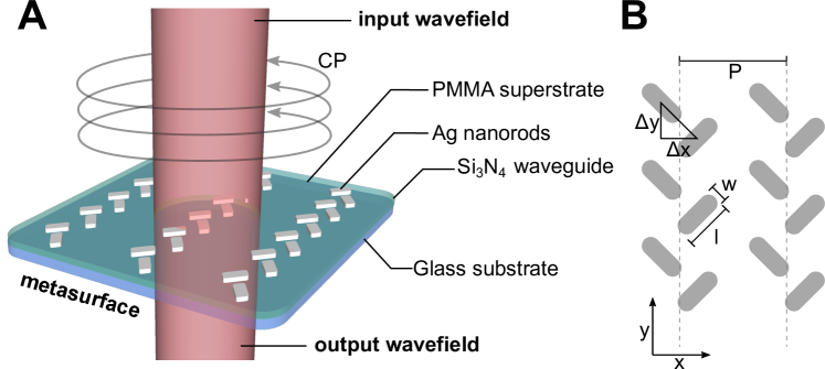
Here we consider a metasurface that consists of an array of Ag nanorods fabricated on a thick Si3N4 waveguide sandwiched between a glass substrate and a PMMA superstrate (Fig. 1a). The nanorods of length and width are arranged in columns with a period as shown in Fig. 1b. Each column consists of two sublattices spaced by in which the nanorods are oriented at and to the -axis. Fradkin et al. Fradkin et al. (2020) showed numerically that this geometry exhibits a transmission asymmetry about normal incidence when illuminated with circularly polarized light. The change in orientation of the nanorods with position appears as a coordinate transformation with respect to the long axes of the rods, in this case a rotation, that varies across the glass surface. Circularly polarised light has an intrinsic spin angular momentum related to the rotation of its electric field vector. Interaction of this spin with the different orientations of the nanorods leads to spin-orbit coupling that generates phase shifts creating an asymmetry in the response of the metasurface Fradkin et al. (2020). In particular, the incident light excites plasmonic dipole resonances that oscillate with a phase difference of due to the phase difference between the - and -polarized components of the incident CP light. Each of the sublattices acts as a grating coupler for the underlying waveguide layer transferring the phase shift of the rod resonances onto the propagating fields in the waveguide. For a separation between the sublattices of , an additional phase shift of is generated between the waveguide modes excited via each sublattice. In this case each sublattice excites guided modes that interfere constructively in one direction, where the phase shifts compensate such that , and destructively in the opposite direction, where . This unidirectional mode propagation creates a process referred to as ‘directional coupling’ Lin et al. (2013). For oblique incidence with the interference condition is offset, enabling an asymmetric angular response of the device. This interference generates the polarization-dependent asymmetric optical transfer function that underpins the phase-imaging method proposed here.
The metasurface investigated here was designed for operation in the red and near-infrared spectral regions and fabricated through an electron beam lithography process that is described in the supplementary material SI2. A scanning electron microscopy (SEM) image of the surface of the device is shown in Fig. 2a. The coupling mechanism of the device is highly sensitive to the geometric parameters of the nanorods. For this reason we obtained averaged values from the SEM images for inclusion in simulations. The resulting parameters for the rod dimensions are and , with the grating periodicity in the and directions , and the spacing of the rods .
The optical response of the metasurface is modelled using the finite element method (FEM), as described in supplement SI3. Fig. 2b shows the calculated transmission spectrum of the device.
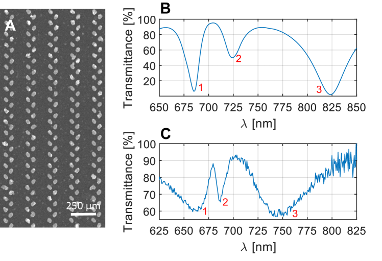
In this configuration the metasurface exhibits three spectral features, with central wavelengths of , and , that suppress transmission at normal incidence for circularly polarized (CP) light (Fig.2b). These features arise from the strong coupling between the TE and TM waveguide modes and the plasmonic electric dipole resonances of the silver nanorods. Experimental measurement of the transmission spectrum through this metasurface shown in Fig.2c, reproduces these spectral features. We attribute the shift in the experimentally measured resonances compared to simulations at , and to differences in the dielectric properties and details of the geometry of the fabricated Si3N4 layer and Ag nanorods as discussed previously. Furthermore, inevitable fabrication inaccuracies arising from the electron beam lithography process are apparent in Fig.2a. Both of these effects alter the plasmonic resonances of the rods as well as the dispersion of the underlying waveguide layer leading to shifts and broadening of the metasurface resonances.
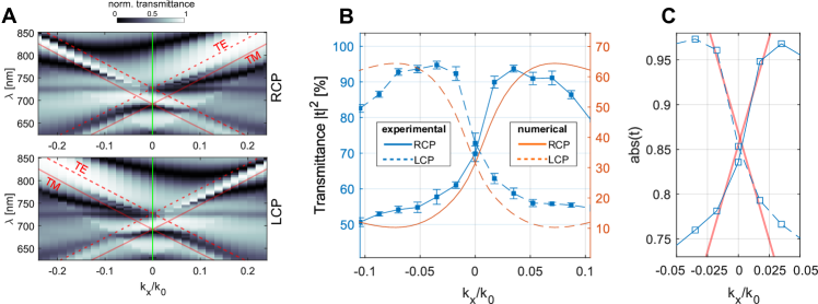
In Fig.3a the simulated transmittance through the device is shown as a function of normalized transverse spatial frequency and free space wavelength with and . Here is the incidence angle of the input beam relative to the surface normal in air. An asymmetric response between positive and negative spatial frequencies is apparent that reverses with a change of the helicity of the circularly polarized incident light. The red lines overlaid on Fig.3a indicate the dispersion of the fundamental TE and TM modes of the slab wavguide, with any variation due to the presence of the plasmonic grating not taken into account. It is apparent that the resonance features of the metasurface are associated with the excitation of the TE and TM modes. Differences between the resonances identified in the FEM calculations and the simple slab waveguide dispersion relations can be attributed to a significant change in the waveguide dispersion due to the presence of the metallic grating and strong coupling between the resonances of the plasmonic nanorods and the waveguide modes. To maximize the sensitivity of the device to spatial frequency we selected operation at the wavelength of the spectral feature marked ’2’ in Figs. 2b,c.
The capacity of the device for asymmetric spatial frequency filtering was experimentally demonstrated by recording transmission spectra as a function of angle of incidence (Fig. 3a). A collimated incident beam from a tungsten halogen lamp is circularly polarized with a linear polarizer and a quarter-wave plate with their respective optical axes oriented at an angle of to obtain LCP or RCP illumination respectively. The transmitted light is collected with a microscope objective and fed into a spectrometer via fiber coupling. Further information about the experimental setup can be found in the supplementary material (SI4). The transmission spectra are normalized to the reference transmittance through an unpatterned region of the sample. In Fig. 3b the measured and calculated transmittance is shown for both LCP and RCP illumination at the wavelength of spectral feature ’2’ - 687 nm. It is apparent that the device provides asymmetric filtering of the Fourier content of an incident field at this wavelength along the -direction. This filter function is essentially one-dimensional with further discussion provided in the supplement (SI1). As discussed, fabrication imperfections lead to the experimentally measured transmittance exhibiting a lower angular filtering contrast than obtained from the FEM result translating to weaker phase-contrast in imaging applications.
To avoid artifacts in the intensity image, the modulation transfer function (MTF) of the system requires a near linear dependence on spatial frequency, accompanied by a negligible variation in the phase transfer function , near the origin. For the metasurface, the experimentally measured MTF shown in Fig. 3c is near-linear over the approximate operational interval [], which is sufficient for phase-imaging of micrometer sized phase objects as demonstrated below. The phase-imaging performance of the metasurface is given by both its numerical aperture, NA, as well as the achievable contrast of across its operational interval It is important to note that the NA of the metasurface refers to the interval of spatial frequencies where the object Fourier transform experiences a linear modification, while the resolution of the imaging system, in which the metasurface is used, will ultimately be given by the NA of the complete optical system.
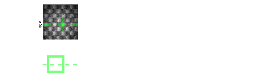
Using this device we demonstrate phase-contrast imaging by transmitting a circularly polarized wavefield with a superimposed phase modulation through the metasurface and recording the transmitted intensity image (Fig. 4b). The phase modulation is generated with a computer controlled spatial light modulator (SLM) with full experimental details provided in the supplementary material (SI5). The phase pattern used in the experiment takes the form of a eggcrate pattern with a normalized spatial frequency of 0.017 superimposed on a uniform background (Fig. 4a). The spatial frequency content of the projected phase distribution hence lies in the linear region of the transfer function. The intensity images obtained upon transmission through the metasurface for incident RCP and LCP light show clear pseudo-3D representations of the phase profile for both polarization states (Fig. 4c,d). These phase images highlight regions of increasing (RCP) and decreasing (LCP) edges of the phase modulation. The edge of the pattern associated with an intensity maximum can be switched via the handedness of the circular polarisation. This effect provides an additional degree of freedom to adjust the phase-contrast. A change from RCP to LCP illumination, therefore, leads to a ‘contrast reversal’ in the pseudo-3D images as indicated in the green inset. Reference images of the wavefield transmitted through an unpatterned region of the substrate are shown on the right side in Fig. 4c,d. With the exception of minor intensity variations attributed to imperfections in the imaging system and the SLM, the phase-modulation is invisible in these reference images. In Fig. 4e lineplots along the green dashed lines in Fig. 4c,d are shown together with the numerically calculated intensity variation for filtering of the of the incident field with the calculated OTF of this metasurface.
Here we have demonstrated the first experimental application to phase contrast imaging of an optical metasurface with an asymmetric transfer function using normally incident light. We showed that the use of photonic spin-orbit coupling to create an asymmetric optical transfer function enables real-time phase-imaging of transmitted wavefields creating pseudo 3D intensity images using circularly polarized light. This new approach opens up intriguing prospects for biological phase imaging. Transparent objects, including live biological cells, placed directly on the metasurface would, in principle, generate intensity relief images similar to those obtained using differential interference microscopy (DIC)Wesemann et al. (2021). Similarly, this approach could be used to visualize refractive index or thickness variations in other transparent media. The real-time, all-optical, phase-imaging properties of the metasurface could be exploited in time-critical applications such as high throughput flow cytometry Picot et al. (2012) or wavefront sensing. Access to asymmetric optical transfer functions is also essential for a broader set of operations in all-optical computation, underpinning mathematical operations including first-order spatial differentiation. Such operations are necessary in high-throughput, real-time image processing situations such as autonomous vehicles, and their execution in the optical domain could alleviate speed and energy consumption limits of electronic signal processing. Finally, the integration of this metasurface approach with photodetectors could enable cost efficient and all-optical image processing for existing camera technology without the requirement for additional bulk-optical components Panchenko et al. (2016).
Funding
The authors acknowledge funding through the Australian Research Council Discovery Projects Scheme (DP160100983) and the Center of Excellence Scheme (CE200100010). This work was performed in part at the Melbourne Centre for Nanofabrication (MCN) in the Victorian Node of the Australian National Fabrication Facility (ANFF).
Supplemental document
See Supplement 1-5 for supporting content.
References
- Park et al. (2018) Y. Park, C. Depeursinge, and G. Popescu, Nature Photonics 12, 578 (2018).
- Arnison et al. (2004) M. R. Arnison, K. G. Larkin, C. J. Sheppard, N. I. Smith, and C. J. Cogswell, Journal of microscopy 214, 7 (2004).
- Zernike (1942) F. Zernike, Physica 9, 686 (1942).
- Ampem-Lassen et al. (2008) E. Ampem-Lassen, F. Sidiroglou, J. L. Peng, S. T. Huntington, and A. Roberts, Optics Express 16, 10912 (2008).
- Marrison et al. (2013) J. Marrison, L. Räty, P. Marriott, and P. O’Toole, Scientific reports 3, 1 (2013).
- Silva et al. (2014) A. Silva, F. Monticone, G. Castaldi, V. Galdi, A. Alù, and N. Engheta, Science 343, 160 (2014).
- Zhu et al. (2017) T. Zhu, Y. Zhou, Y. Lou, H. Ye, M. Qiu, Z. Ruan, and S. Fan, Nature Communications 8, 1 (2017).
- Dong et al. (2018) Z. Dong, J. Si, X. Yu, and X. Deng, Applied Physics Letters 112, 181102 (2018).
- Guo et al. (2018) C. Guo, M. Xiao, M. Minkov, Y. Shi, and S. Fan, Optica 5, 251 (2018).
- Bykov et al. (2018) D. A. Bykov, L. L. Doskolovich, A. A. Morozov, V. V. Podlipnov, E. A. Bezus, P. Verma, and V. A. Soifer, Optics Express 26, 10997 (2018).
- Cordaro et al. (2019) A. Cordaro, H. Kwon, D. Sounas, A. Koenderink, A. Alù, and A. Polman, Nano Letters 19, 8418 (2019).
- Zhu et al. (2019) T. Zhu, Y. Lou, Y. Zhou, J. Zhang, J. Huang, Y. Li, H. Luo, S. Wen, S. Zhu, Q. Gong, et al., Physics Review Applied 11, 034043 (2019).
- He et al. (2020) S. He, J. Zhou, S. Chen, W. Shu, H. Luo, and S. Wen, APL Photonics 5, 5144953 (2020).
- Zhou et al. (2020a) Y. Zhou, W. Wu, R. Chen, W. Chen, R. Chen, and Y. Ma, Advanced Optical Materials 8, 1901523 (2020a).
- Zhou et al. (2020b) Y. Zhou, H. Zheng, I. I. Kravchenko, and J. Valentine, Nature Photonics 14, 316 (2020b).
- Wesemann et al. (2019) L. Wesemann, E. Panchenko, K. Singh, E. D. Gaspera, D. E. Gómez, T. J. Davis, and A. Roberts, APL Photonics 4, 100801 (2019).
- Vohnsen and Valente (2015) B. Vohnsen and D. Valente, Optica 2, 1024 (2015).
- Zhu et al. (2020) T. Zhu, J. Huang, and Z. Ruan, Advanced Photonics 2, 016001 (2020).
- Wesemann et al. (2021) L. Wesemann, J. Rickett, J. Song, J. Lou, E. Hinde, T. J. Davis, and A. Roberts, Light: Science & Applications 10, 1 (2021).
- Bliokh et al. (2015) K. Bliokh, F. Rodriguez-Fortuno, F. Nori, and A. Zayats, Nature Photonics 9, 796 (2015).
- Davis et al. (2019) T. J. Davis, F. Eftekhari, D. E. Gómez, and A. Roberts, Phyical Review Letters 123, 013901 (2019).
- Fradkin et al. (2020) I. M. Fradkin, S. A. Dyakov, and N. A. Gippius, Physical Review B 102, 045432 (2020).
- Lin et al. (2013) J. Lin, J. B. Mueller, Q. Wang, G. Yuan, N. Antoniou, X.-C. Yuan, and F. Capasso, Science 340, 331 (2013).
- Picot et al. (2012) J. Picot, C. L. Guerin, C. Le Van Kim, and C. M. Boulanger, Cytotechnology 64, 109 (2012).
- Panchenko et al. (2016) E. Panchenko, J. J. Cadusch, T. D. James, and A. Roberts, ACS Photonics 3, 1833 (2016).