Weak antilocalization and Shubnikovde Haas oscillations in CaCuSb single crystal
Abstract
Quantum oscillations in both linear and Hall resistivities and weak antilocalization (WAL) are barely observed in bulk single crystals. Here we report the transport properties of a CaCuSb single crystal that crystallizes in the hexagonal crystal structure. The magnetotransport studies reveal WAL and Shubnikovde Haas (SdH) quantum oscillations with a unique frequency at T. A cusp-like behavior in the low field regime of magnetotransport for -plane and [0001] confirms the WAL in CaCuSb. Angular-dependent normalized magnetoconductance and SdH oscillations studies reveal that the observed phenomena originate from the transport channels. The high magnetic field (up to T) experiments demonstrate plateau-like features in the Hall measurements. The first-principles calculations unfold that CaCuSb is a non-topological semimetal with dominant hole carries at the Fermi level. Our study reveals that CaCuSb is a promising candidate to explore the quasi quantum transport phenomenon in the transition metal pnictide materials.
I INTRODUCTION
Since the discovery of topological insulators (TIs) with nontrivial metallic surface states Hasan and Kane (2010); Moore (2010), substantial research efforts are devoted in searching new topological semimetals owing to their novel electronic structure and interesting physical properties Hu et al. (2019); Burkov (2016); Wang et al. (2018); Zhang et al. (2017); Berger et al. (2018); Wu et al. (2019); Hao et al. (2018); Cai et al. (2018). Following the foot-print of graphene Meyer et al. (2007), materials are widely investigated due to their exotic transport properties which seed from carrier confinement effects Zhang et al. (2019); Pi et al. (2019). It has been found that in addition to materials, the topological materials with layered crystal structure also show the behavior of carriers. In this regard, the transition metal-pnictides layered ternary compounds of -type offer a prominent setup for realizing exotic topological and transport propertiesSingh et al. (2018); Mardanya et al. (2019); Sasmal et al. (2020). For example, CaAgBi Sasmal et al. (2020) exhibits Dirac-Weyl semimetal with weak antilocalization (WAL) effects, whereas LuPdBi Pavlosiuk et al. (2015) and YPtBi Butch et al. (2011) exhibit WAL as well as superconductivity at low temperature. When the phase coherence length () is larger than the mean free path (), quantum interference results in either the weak localization (WL) or WAL effects depending on whether the interference is constructive or destructive, respectively Lu and Shen (2014); Datta (1995); Zhao et al. (2019a). The strong spin-orbit coupling (SOC) effects lead to spin-rotation in materials whenever an electron gets scattered due to impurity, and thereby causing the phase change of the electron wave function, realizing a destructive interference. The destructive interference enhances the conductivity and a cusp-like negative conductivity is observed in the single crystals of various ternary materials Shrestha et al. (2017); Sasmal et al. (2020); Laha et al. (2019). At a sufficiently high magnetic field, if the system is in a quantum diffusive regime (), the Fermi energy crosses the Landau levels with increasing field, leading to Shubnikovde Haas (SdH) oscillations in the magnetoresistance. There are a few reports that show both the WAL and quantum oscillations in longitudinal resistivity, although oscillations in Hall data are usually absent in those materials Bao et al. (2012); Bhardwaj et al. (2018).
In this study, we report magnetotransport properties and demonstrate the WAL and SdH quantum oscillations in both the linear and Hall resistivities in a single crystal of . CaCuSb belongs to a large family of -type hexagonal materials with the space group (No. 194). A cusp-like behavior is observed in the low field region of magnetoresistance (MR), confirming the WAL effect in CaCuSb. At sufficiently high magnetic fields, SdH oscillations are observed which enable us to reveal its conduction and Fermi surface properties. Interestingly, the Hall effect measurements show the signatures of Hall plateaus at definite intervals. Our analyses suggest that the observed transport phenomena in are due to the quasi- transport channels in the layered crystal structure, consisting of Cu-Sb layers that are separated by Ca layers.
II Experimental Methods
Good quality single crystals of CaCuSb were synthesized by flux method using Cu:Sb eutectic composition as a flux. High purity starting elements of Ca (99.98% ingot from Alfa Aesar), Cu (99.999% shot from Alfa Aesar) and Sb (99.999% shot from Alfa Aesar) were taken in 1:4.5:7.5 molar ratio in an alumina crucible. The alumina crucible was sealed in a quartz ampoule under a partial pressure of Ar gas. The sealed ampoule was placed in a box type furnace, and heated to 1050∘C at the rate of 30∘C/h and held at this temperature for 24 h, for proper homogenization. Then the furnace was allowed to slow cool at the rate of 2∘C/h to 630∘C at which point the flux was removed by centrifuging. Electrical transport studies have been performed on a cut and aligned bar-shaped sample with current along the principle crystallographic directions in the basal plane and along the -axis. Electrical transport measurements were carried out on a sample with dimension mm3, using Quantum Design Physical Property Measurement System (PPMS) instrument with magnetic field up to 14 T, in the temperature range K. High magnetic field Hall effect measurement was performed at the European Magnetic Field Laboratory (EMFL) at the Laboratoire National des Champs Magnétiques Intenses (LNCMI) at Toulouse, France, up to a mangetic field of T.
III Results and Discussions
III.1 X-ray diffraction
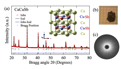
The room temperature powder x-ray diffraction (XRD) and Rietveld refinement of the XRD data are shown in Fig. 1(a). From the refinement we estimate the lattice parameters as Å and Å which are in good agreement with the previously published data Eisenmann et al. (1974). The Rietveld analysis also confirmed the space group as (No. 194) and the Wyckoff positions of Ca, Cu, and Sb as , and respectively. The crystal structure of CaCuSb is shown in the inset of Fig. 1(a). It is evident that the crystal structure is layered along the hexagonal -axis where CuSb layers are sandwiched between Ca-layers and each CuSb layer is rotated by relative to the neighbouring layer. These CuSb layers may act as a unique charge transport layers which are confined in the -plane. As grown single crystal with the flat plane corresponding to (0001) is shown in Fig 1(b). The Laue diffraction pattern of the flat plane is shown in Fig. 1(c). Well defined Laue diffraction pattern together with the -fold symmetry confirms the good quality of the single crystal.

III.2 Electrical transport and Hall resistivity
The temperature dependence of electrical resistivity is shown in Fig 2(a) for both in-plane () and out-of-plane () current directions which shows a metallic nature. The electrical resistivity is anisotropic depending on the direction of the current flow and a large anisotropy is observed for in-plane and out-of-plane current directions, thus it refers to a quasi- nature of the electrical transport. Figure 2(b) shows the magnetoresistance (MR) at K, for [12̄10] (-plane) and [0001], showing a cusp-like behavior that increases rapidly at low fields and linearly above T, and the MR reaches 41% at 14 T. This cusp-like behavior in MR is reminiscent of the WAL effect seen in similar equiatomic systems He et al. (2011); Liu et al. (2012); Sasmal et al. (2020); Pavlosiuk et al. (2015); Butch et al. (2011). Generally, the WAL phenomenon is observed due to charge diffusion in the system. However, the presence of such WAL for [12̄10] here suggests the possibility of destructive interference in the - plane. For [0001] and [101̄0], MR is 3.5% at 14 T (12 times smaller than -plane) and almost linear in the entire field range without any sign of WAL in this direction, indicating the absence of such interference effects. These results support that the observed WAL has a nature. The WAL behavior vanishes for , as shown in the Supplemental Material Figure S1 sup . Furthermore, in the range of T, SdH oscillation has been observed for [12̄10] and [0001], but it is absent for [0001] and [101̄0]. Here, we have symmetrized the linear resistivity and antisymmetrized the Hall resistivity . The Hall resistivity is measured in a pulsed magnetic field of T at K is shown in Fig. 2(c), which remains positive, suggesting that the hole carriers are dominant in the system. From the slope of Hall resistivity we estimate the carrier density and the mobility using a single band model as m-3 and m2V-1s-1, respectively. The two-band model gives contribution from both the electron and hole (See Supplemental Material Figure S2 sup ).
III.3 Weak antilocalization
The calculated magnetoconductivity (MC), with , for [12̄10] and is shown in Fig. 2(d). It is obvious that the calculated MC also exhibits a cusp-like feature suggesting WAL in this quasi- CaCuSb. Usually, this cusp-like feature can be seen at very low field for low dimensional systems. In the present case at T, the value of , which is less than 1, where and s, and is the electronic charge (the quantum parameters and have been obtained from the SdH oscillations, as discussed later). This suggests the charge transport is in quantum diffusive regime, so that WAL has been observed even at T. Notably, the observed WAL in MC at low fields can be explained based on the Hikami-Larkin-Nagaoka (HLN) model Hikami et al. (1980). In the strong SOC limit, the HLN model is given as
| (1) |
where , , and are the electronic charge, digamma function, and phase coherence length, respectively. From this HLN fit, the phase coherence length is estimated as nm and m-1 (shown in in Fig 2(d)). Here, indicates the number of conduction channels per unit length. Considering the sample thickness of 120 , the obtained total conduction channels in the system is . Such a large number of conduction channels has been reported in several semimetallic systems like Bi2Te3 Shrestha et al. (2017), YbCdGe Laha et al. (2019), LuPdBi Pavlosiuk et al. (2015), YPtBi Pavlosiuk et al. (2016). Temperature dependence of phase coherence length () is shown in Fig 2(e). Because of phononic contribution the decreases with increasing temperature and it can be described by the relation
| (2) |
where the zero temperature phase coherence length, and and are the electron-electron and electron-phonon contribution, respectively. The obtained fitting parameters are nm, nm and nm. The coefficient is almost constant through the temperature regime K, this suggests the number of conduction channels are almost unaltered with temperature. Furthermore, we have also performed the angular dependence of MC at K to understand the origin of WAL (Fig. 2(f)). The normalized MC (Normalized) is plotted as a function at different tilt angles ( is the angle between the direction of current and magnetic field). The vs plot shows that the low field MC falls onto a single curve for all the measured field angles. This suggests that WAL effect is originated from parallel conduction channels in the bulk Chen et al. (2011); Shrestha et al. (2017); Xu et al. (2014). Similar behavior of MC curve is seen in other measured samples (Supplemental Material Figure S3 sup ). The parallel conduction channels are presumably due to the CuSb layers which is further confirmed from the band structure studies (to be discussed later) where the density-of-states (DOS) of the Cu and Sb atoms is much higher than Ca atoms at the Fermi level.
III.4 Shubnikovde Haas (SdH) quantum oscillations
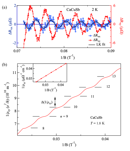
It is interesting to note that the longitudinal resistance of CaCuSb at sufficiently large magnetic fields () oscillates periodically in , depicting SdH quantum oscillations. The raw SdH oscillation observed in the field range T at K is shown in Fig. 3(a). We further obtain SdH frequency by subtracting the background signal using a polynomial function and plot vs in the top inset of Fig. 3(a). A simple fast Fourier transform (FFT) of as a function of reveals a unique frequency at T. A similar quantum oscillation in linear resistivity has been observed on a different sample B2, see Figure S4 in Supplemental Material sup . From the Onsager relation we have estimated extremal area of the Fermi surface, where is quantum of flux. and FFT amplitude at different temperatures are shown in Fig 3(b)-(c). The oscillating part of the has been analyzed using the standard Lifshitz-Kosevich (LK) equation which is given by Shoenberg (2009)
| (3) |

| 0.0652 | 0.4 | 8 | 1.5 |
Here, is the field induced damping factor where is a constant, is the frequency of oscillation, and is the Dingle temperature. is the thermal damping factor given by the LK formula where and is the phase shift that includes Berry phase information. The temperature variation of the FFT amplitude is fitted to thermal damping factor which resulted in an effective carrier mass . From the slope of vs plot, where sinh(X), we obtain the Dingle temperature () as K (Fig. 3 (d)). The carrier life time and mobility are also estimated. All the parameters obtained from SdH oscillations are listed in Table 1. To confirm the quasi- nature of CaCuSb, we have performed the angular dependence of SdH oscillation, as shown in Fig. 3(e), where the angle represents the angle between magnetic field and current. However, as given in Ref. Xiang et al. (2015); Zhao et al. (2019b, a), there is another approach of rotation of sample which can also give the Fermi surface information. The angular dependence of the FFT frequency obtained from the experimentally observed quantum oscillations is shown as black filled square in Fig. 3(f). For angles below , the quantum oscillations are not discernible. This suggests a possibility of an elongated ellipsoidal Fermi surface at the center of the Brillouin zone. A much larger magnetic field and lower temperature are necessary to observe the SdH oscillations at low angles and oscillations from other Fermi pockets as well. The calculated quantum oscillations using first-principles Fermi surface are shown in Fig. 3(f) (see Sec. III.5 for discussion on Fermi surface). From the detailed band structure calculations, we find that the Brillouin zone contains two hole pockets centered at point and small electron pockets located at the point (see Fig. 5). The calculated quantum oscillations frequency for is 305 T (40 T) for outer (inner) hole pocket and 160 T for the electron pockets. The extremal area for the outer (inner) hole pocket is m-2 ( m-2) and for the electron pocket is m-2. The experimentally observed frequency of 314 T corresponds to an area of m-2. These results indicate the central large hole pocket at point is compatible with the experimental SdH oscillation for [12̄10] and . Furthermore, a detailed comparison of our experimental results shows that the observed Fermi pocket may have an elongated ellipsoidal shape. The anisotropy in the Fermi surface is very well reflected in the large anisotropy in the electrical resistivity (Fig. 2(a)) where is larger than , suggesting a quasi- character.
Background subtracted (right axis) and (left axis) are shown in Fig 4(a). It is evident from the figure that quantum oscillations are observed even for the Hall resistance , however there is a phase shift of about between and . Interestingly, at sufficiently high magnetic fields ( T T), the Hall resistivity shows step-like features (plateaus) in the vs and the plateau size corresponding to two consecutive steps is = m-1 (Fig 4(b)). In Fig 4(b), refers to the LL index which is obtained from where is the frequency of the quantum oscillation and is the field at which shows minimum in the oscillations. The oscillations observed in Hall data up to a magnetic field of 45 T also have the FFT frequency of 314 T. For multilayer quantum Hall effect, the step size of inverse Hall resistivity can be written as , where is the average conduction channels per unit thickness contributing to this multilayer transport. If we assume these parallel conduction channels result in the observed plateau-like feature in the Hall measurement, then the step size in the scale of is m-1. From the value, we can calculate the bulk carrier density which matches well with the bulk carrier density estimated from the slope of the Hall resistivity data (). From the HLN model, the obtained average number of conduction channels per unit thickness is m-1, which is nearly similar to the average number of conduction channels () obtained from the Hall plateau. Even at such high magnetic fields, no additional frequency or any kind of peak splitting is observed (see Supplementary Materials Fig. S5 sup ). The step-like features observed in Fig. 4(b) are something similar to quantized Hall plateaus with high filling factor Xu et al. (2017); Sasaki et al. (1999). Additionally, the phase difference between and , and for , indicating the quantum Hall regime. All these suggest that the observed steps in the Hall data may be due to quantum Hall effect. The linearity in the () plot (Fig. 4(b)) gives additional testimony for the quantization nature of the Hall effect. Notably, the quantized Hall steps in systems are usually attributed to the parallel conduction channels and have been observed in various layered bulk systems such as Bi2Se3 Cao et al. (2012); Busch et al. (2018), HfTe5 Galeski et al. (2020), and EuMnBi2 Masuda et al. (2016). CaCuSb possesses a layered crystal structure where the Cu-Sb layers are separated by Ca layers. Our experimental results and band structure calculations also indicate that the Cu-Sb layers act as conduction channels, which leads to the observation of Hall plateaus in CaCuSb.

III.5 Band structure of CaCuSb
First-principles calculations were performed based on the density-functional theory Hohenberg and Kohn (1964) with the projector augmented wave (PAW) method Blöchl (1994), as implemented in the Vienna simulation package (VASP) Kresse and Furthmüller (1996); Kresse and Joubert (1999). The generalized gradient approximation (GGA) was used for the exchange-correlation effects Perdew et al. (1996). The SOC was considered self-consistently. A plane wave cutoff energy of 420 eV was used and a -centered mesh was employed to sample bulk Brillouin zone. The FermiSurfer program was used to visualize the Fermi surface Kawamura (2019). We present the calculated band structure CaCuSb in Fig. 5(a). It is seen to be semimetallic in which small electron pockets located at overlap in energy with the large hole bands centered at the point. The orbital resolved band structure shows that hole bands are dominated by Sb states whereas the electron bands near the Fermi level are mainly composed of Cu states. Notably, the bands do not constitute a band inversion, showing that CaCuSb is a nontopological semimetal. The density of states (DOS) in Fig. 5(b) further reveal a small DOS at the Fermi level which is a reminiscent feature of the semimetallic state. Nevertheless, we find that Ca has vanishing DOS whereas the Cu-Sb has notable DOS at the Fermi level. The Fermi surface is shown in Fig. 5(c) where the color scale marks the Fermi velocity on each band. It consists of a big ellipsoidal shaped hole pocket with a major axis along the hexagonal axis and three small electron pockets at the points. Importantly, the Fermi velocity is higher for the hole bands whereas it is minimum for the electron pockets. This is in accord with the dominant hole-carriers observed in our experimental samples. Furthermore, the finite Cu-Sb states constituted hole bands with relatively higher DOS at the Fermi level. It should be noted that both the Cu and Sb atoms have large SOC which splits the Sb states, leading to two-hole pockets at the -point. Thus, while the system is topologically trivial, due to inherent large SOC, it can show WAL as seen in our experiments as well as reported widely in other materials Hu et al. (2014); Bergmann (1984); Lin and Bird (2002).
IV Summary
In summary, the flux-grown CaCuSb single crystal exhibits a huge anisotropy in electrical transport. This anisotropy can be related to the layered crystal structure where the two CuSb layers are separated by Ca-layers of the hexagonal unit cell. WAL and quantum oscillations have been observed in the linear and Hall resistivities. The WAL behavior is confirmed from the magnetotransport and low field magnetoconductance analysis. Interestingly, the SdH oscillation is observed in the field range T with a frequency at T, which is primarily due to the large hole-pocket centered at - point. Low field normalized magnetoconductance falls onto a single curve for different angles and SdH oscillation vanishes below 60∘ suggest the quasi- nature of the electrical transport. The high magnetic field Hall resistivity data exhibits step-like features at regular intervals. The angular-dependent magnetoconductance, anisotropy in magnetoresistance, and band structure indicate the presence of multiple conduction channels. First-principles calculations have revealed that CaCuSb is a normal semimetal with dominant hole carriers and higher CuSb DOS at the Fermi level. A comparison of calculated quantum oscillations with the observed oscillations suggests that the Fermi pockets may have an elongated ellipsoidal shape. It is clear from these results that although CaCuSb possesses a layered structure, it can be considered as a pseudo- system. The present study would pave way for identifying layered materials as a new platform to investigate quasi- transport properties.
V ACKNOWLEDGEMENTS
We thank Department of Atomic Energy (DAE) of Government of India for financial support. We also acknowledge the support of the LNCMI-CNRS,member of the European Magnetic Field Laboratory (EMFL) for high magnetic field measurements.
References
- Hasan and Kane (2010) M. Z. Hasan and C. L. Kane, Rev. Mod. Phys. 82, 3045 (2010).
- Moore (2010) J. E. Moore, Nature 464, 194 (2010).
- Hu et al. (2019) J. Hu, S.-Y. Xu, N. Ni, and Z. Mao, Annu. Rev. Mater. Res. 49, 207 (2019).
- Burkov (2016) A. A. Burkov, Nat. Mater. 15, 1145 (2016).
- Wang et al. (2018) H. Wang, Y. Chen, M. Duchamp, Q. Zeng, X. Wang, S. H. Tsang, H. Li, L. Jing, T. Yu, E. H. T. Teo, and Z. Liu, Adv. Mater. 30, 1704382 (2018).
- Zhang et al. (2017) Z. Zhang, J. Niu, P. Yang, Y. Gong, Q. Ji, J. Shi, Q. Fang, S. Jiang, H. Li, X. Zhou, L. Gu, X. Wu, and Y. Zhang, Adv. Mater. 29, 1702359 (2017).
- Berger et al. (2018) A. N. Berger, E. Andrade, A. Kerelsky, D. Edelberg, J. Li, Z. Wang, L. Zhang, J. Kim, N. Zaki, J. Avila, C. Chen, M. C. Asensio, S.-W. Cheong, B. A. Bernevig, and A. N. Pasupathy, npj Quantum Mater. 3, 2 (2018).
- Wu et al. (2019) F. Wu, C. Guo, M. Smidman, J. Zhang, Y. Chen, J. Singleton, and H. Yuan, npj Quantum Mater. 4, 20 (2019).
- Hao et al. (2018) S. Hao, J. Zeng, T. Xu, X. Cong, C. Wang, C. Wu, Y. Wang, X. Liu, T. Cao, G. Su, L. Jia, Z. Wu, Q. Lin, L. Zhang, S. Yan, M. Guo, Z. Wang, P. Tan, L. Sun, Z. Ni, S.-J. Liang, X. Cui, and F. Miao, Adv. Funct. Mater. 28, 1803746 (2018).
- Cai et al. (2018) S. Cai, J. Guo, V. A. Sidorov, Y. Zhou, H. Wang, G. Lin, X. Li, Y. Li, K. Yang, A. Li, Q. Wu, J. Hu, S. K. Kushwaha, R. J. Cava, and L. Sun, npj Quantum Mater. 3, 62 (2018).
- Meyer et al. (2007) J. C. Meyer, A. K. Geim, M. I. Katsnelson, K. S. Novoselov, T. J. Booth, and S. Roth, Nature 446, 60 (2007).
- Zhang et al. (2019) Y. Zhang, Y. Yao, M. G. Sendeku, L. Yin, X. Zhan, F. Wang, Z. Wang, and J. He, Adv. Mater. 31, 1901694 (2019).
- Pi et al. (2019) L. Pi, L. Li, K. Liu, Q. Zhang, H. Li, and T. Zhai, Adv. Funct. Mater. 29, 1904932 (2019).
- Singh et al. (2018) B. Singh, S. Mardanya, C. Su, H. Lin, A. Agarwal, and A. Bansil, Phys. Rev. B 98, 085122 (2018).
- Mardanya et al. (2019) S. Mardanya, B. Singh, S.-M. Huang, T.-R. Chang, C. Su, H. Lin, A. Agarwal, and A. Bansil, Phys. Rev. Mater. 3, 071201 (2019).
- Sasmal et al. (2020) S. Sasmal, R. Mondal, R. Kulkarni, A. Thamizhavel, and B. Singh, J. Phys.: Condens. Matter 32, 335701 (2020).
- Pavlosiuk et al. (2015) O. Pavlosiuk, D. Kaczorowski, and P. Wiśniewski, Sci. Rep. 5, 9158 (2015).
- Butch et al. (2011) N. P. Butch, P. Syers, K. Kirshenbaum, A. P. Hope, and J. Paglione, Phys. Rev. B 84, 220504 (2011).
- Lu and Shen (2014) H.-Z. Lu and S.-Q. Shen, Proc. SPIE 9167, Spintronics VII, 91672E, 9167, 263 (2014).
- Datta (1995) S. Datta, Electronic Transport in Mesoscopic Systems, Cambridge Studies in Semiconductor Physics and Microelectronic Engineering (Cambridge University Press, 1995).
- Zhao et al. (2019a) W. Zhao, L. Chen, Z. Yue, Z. Li, D. Cortie, M. Fuhrer, and X. Wang, npj Quantum Mater. 4, 56 (2019a).
- Shrestha et al. (2017) K. Shrestha, M. Chou, D. Graf, H. D. Yang, B. Lorenz, and C. W. Chu, Phys. Rev. B 95, 195113 (2017).
- Laha et al. (2019) A. Laha, S. Malick, R. Singha, P. Mandal, P. Rambabu, V. Kanchana, and Z. Hossain, Phys. Rev. B 99, 241102 (2019).
- Bao et al. (2012) L. Bao, L. He, N. Meyer, X. Kou, P. Zhang, Z.-g. Chen, A. V. Fedorov, J. Zou, T. M. Riedemann, T. A. Lograsso, K. L. Wang, G. Tuttle, and F. Xiu, Sci. Rep. 2, 726 (2012).
- Bhardwaj et al. (2018) V. Bhardwaj, S. P. Pal, L. K. Varga, M. Tomar, V. Gupta, and R. Chatterjee, Sci. Rep. 8, 9931 (2018).
- Eisenmann et al. (1974) B. Eisenmann, G. Cordier, and H. Schäfer, Z. Naturforsch. B 29, 457 (1974).
- He et al. (2011) H.-T. He, G. Wang, T. Zhang, I.-K. Sou, G. K. L. Wong, J.-N. Wang, H.-Z. Lu, S.-Q. Shen, and F.-C. Zhang, Phys. Rev. Lett. 106, 166805 (2011).
- Liu et al. (2012) M. Liu, J. Zhang, C.-Z. Chang, Z. Zhang, X. Feng, K. Li, K. He, L.-l. Wang, X. Chen, X. Dai, Z. Fang, Q.-K. Xue, X. Ma, and Y. Wang, Phys. Rev. Lett. 108, 036805 (2012).
- (29) See Supplemental Material for Temperature dependent magnetoresistance, weak antilocalization and Shubnikov-de Haas oscillation in different sample .
- Hikami et al. (1980) S. Hikami, A. I. Larkin, and Y. Nagaoka, Prog. Theor. Phys. 63, 707 (1980).
- Pavlosiuk et al. (2016) O. Pavlosiuk, D. Kaczorowski, and P. Wiśniewski, Phys. Rev. B 94, 035130 (2016).
- Chen et al. (2011) J. Chen, X. Y. He, K. H. Wu, Z. Q. Ji, L. Lu, J. R. Shi, J. H. Smet, and Y. Q. Li, Phys. Rev. B 83, 241304 (2011).
- Xu et al. (2014) G. Xu, W. Wang, X. Zhang, Y. Du, E. Liu, S. Wang, G. Wu, Z. Liu, and X. X. Zhang, Sci. Rep. 4, 5709 (2014).
- Shoenberg (2009) D. Shoenberg, Magnetic oscillations in metals (Cambridge university press, 2009).
- Xiang et al. (2015) F.-X. Xiang, X.-L. Wang, M. Veldhorst, S.-X. Dou, and M. S. Fuhrer, Phys. Rev. B 92, 035123 (2015).
- Zhao et al. (2019b) W. Zhao, D. Cortie, L. Chen, Z. Li, Z. Yue, and X. Wang, Phys. Rev. B 99, 165133 (2019b).
- Xu et al. (2017) S. Xu, J. Shen, G. Long, Z. Wu, Z.-q. Bao, C.-C. Liu, X. Xiao, T. Han, J. Lin, Y. Wu, H. Lu, J. Hou, L. An, Y. Wang, Y. Cai, K. M. Ho, Y. He, R. Lortz, F. Zhang, and N. Wang, Phys. Rev. Lett. 118, 067702 (2017).
- Sasaki et al. (1999) M. Sasaki, N. Miyajima, H. Negishi, S. Negishi, M. Inoue, H. Kadomatsu, and G. Machel, Solid State Commun. 109, 357 (1999).
- Cao et al. (2012) H. Cao, J. Tian, I. Miotkowski, T. Shen, J. Hu, S. Qiao, and Y. P. Chen, Phys. Rev. Lett. 108, 216803 (2012).
- Busch et al. (2018) M. Busch, O. Chiatti, S. Pezzini, S. Wiedmann, J. Sánchez-Barriga, O. Rader, L. V. Yashina, and S. F. Fischer, Sci. Rep. 8, 485 (2018).
- Galeski et al. (2020) S. Galeski, X. Zhao, R. Wawrzyńczak, T. Meng, T. Förster, P. M. Lozano, S. Honnali, N. Lamba, T. Ehmcke, A. Markou, Q. Li., G. Gu, W. Zhu, J. Wosnitza, C. Felser, G. F. Chen, and J. Gooth, Nat. Commun. 11, 5926 (2020).
- Masuda et al. (2016) H. Masuda, H. Sakai, M. Tokunaga, Y. Yamasaki, A. Miyake, J. Shiogai, S. Nakamura, S. Awaji, A. Tsukazaki, H. Nakao, Y. Murakami, T.-h. Arima, Y. Tokura, and S. Ishiwata, Sci. Adv. 2, 10.1126/sciadv.1501117 (2016).
- Hohenberg and Kohn (1964) P. Hohenberg and W. Kohn, Phys. Rev. 136, B864 (1964).
- Blöchl (1994) P. E. Blöchl, Phys. Rev. B 50, 17953 (1994).
- Kresse and Furthmüller (1996) G. Kresse and J. Furthmüller, Phys. Rev. B 54, 11169 (1996).
- Kresse and Joubert (1999) G. Kresse and D. Joubert, Phys. Rev. B 59, 1758 (1999).
- Perdew et al. (1996) J. P. Perdew, K. Burke, and M. Ernzerhof, Phys. Rev. Lett. 77, 3865 (1996).
- Kawamura (2019) M. Kawamura, Comput. Phys. Commun. 239, 197 (2019).
- Hu et al. (2014) J. Hu, J. Y. Liu, and Z. Q. Mao, J. Phys.: Condens. Matter 26, 095801 (2014).
- Bergmann (1984) G. Bergmann, Phys. Rep. 107, 1 (1984).
- Lin and Bird (2002) J. J. Lin and J. P. Bird, J. Phys.: Condens. Matter 14, R501 (2002).