2Argonne National Laboratory, 9700 South Cass Avenue., Argonne, IL, 60439, USA
3Kavli Institute for Cosmological Physics, U. Chicago, 5640 South Ellis Avenue, Chicago, IL, 60637, USA
4Fermi National Accelerator Laboratory, MS209, P.O. Box 500, Batavia, IL, 60510, USA
5Department of Physics, McGill University, 3600 Rue University, Montreal, Quebec H3A 2T8, Canada
6Harvard-Smithsonian Center for Astrophysics, 60 Garden Street, Cambridge, MA, 02138, USA
Development of MKIDs for measurement of the Cosmic Microwave Background with the South Pole Telescope
Abstract
We present details of the design, simulation, and initial test results of prototype detectors for the fourth-generation receiver of the South Pole Telescope (SPT). Optimized for the detection of key secondary anisotropies of the cosmic microwave background (CMB), SPT-3G+ will measure the temperature and polarization of the mm/sub-mm sky at 220, 285, and 345 GHz, beyond the peak of the CMB blackbody spectrum. The SPT-3G+ focal plane will be populated with microwave kinetic inductance detectors (MKIDs), allowing for significantly increased detector density with reduced cryogenic complexity. We present simulation-backed designs for single-color dual-polarization MKID pixels at each SPT-3G+ observation frequency. We further describe design choices made to promote resonator quality and uniformity, enabling us to maximize the available readout bandwidth. We also discuss aspects of the fabrication process that enable rapid production of these devices and present an initial dark characterization of a series of prototype devices.
Keywords:
CMB, kinetic inductance detectors, SPT, microwave instrumentation1 Introduction
The South Pole Telescope (SPT) is a 10-meter diameter mm/sub-mm wave telescope designed to measure the cosmic microwave background (CMB) and make new discoveries in high energy physics, astrophysics, and cosmology (e.g.,[3, 14, 11]). The SPT is currently equipped with the SPT-3G camera [6], which is populated by an array of trichroic pixels made up of transition-edge sensor (TES) bolometers observing at 95, 150, and 220 GHz [6]. At the conclusion of the SPT-3G survey, the camera will be replaced by SPT-3G+, the fourth-generation receiver and focal plane, which is shown schematically in Figure 1. Observing the same 1500 square degree field as its predecessor, SPT-3G+ will enable high-sensitivity measurements of the temperature and polarization of the mm/sub-mm sky at observing frequencies of 225, 285, and 345 GHz, beyond the peak of the CMB blackbody spectrum. In combination with the SPT-3G data, SPT-3G+ will target new cosmological observables such as the patchy kinematic Sunyaev-Zel’dovich effect [21] and the Rayleigh scattering of the CMB [16]. Robust detection of these observables will lead to groundbreaking constraints on the duration and timing of the epoch of reionization [1], and provide new insights on the expansion of the universe just after recombination [7]. While tantalizing from a science perspective, these signals are less than a few percent of the amplitude of the primary CMB signal, and their detection requires an experiment with sensitivity beyond that which is presently available. The sensitivity of superconducting TESs for CMB observation is no longer limited by individual detector noise, but by temporal fluctuations in the incident photon signal (photon noise). Therefore, to achieve the increased sensitivity required to meet the SPT-3G+ science goals, a higher density of detectors on the focal plane is necessary. The detector density of the SPT-3G focal plane is now approaching a practical limit due to the number of wires that are needed to bias and readout each detector [6]. The drive for even greater detector density motivates the use of a more multiplexable CMB detector technology on the SPT-3G+ focal plane .

Microwave kinetic inductance detectors (MKIDs) offer an attractive alternative solution, allowing for increased detector densities with significantly reduced readout complexity and more straightforward fabrication. These advantages combine to enable the construction of large-format arrays of MKIDs with the necessary detector density for SPT-3G+ sensitivity requirements. Due to their resonator-based design, MKIDs are highly multiplexable and have the further advantage that they require no additional cryogenic multiplexing electronics - each detector has a characteristic readout frequency set by the geometry of its resonator. The fundamental limit for the MKID multiplexing (MUX) factor is set by the quality factor of the resonator, where a higher quality factor equates to a lower required readout bandwidth for a given detector. While individual MKIDs have been fabricated with extremely high quality factors [24] [2], the on-sky operation of a large MKID array presents important challenges with respect to the achievable channel densities. Previous mm-wave experiments have operated MKID arrays with detector counts of roughly 200 [8], 1000 [5], and 3000 [12]. The stage is now set for the creation of an operational mm-wave MKID array with tens of thousands of detectors.
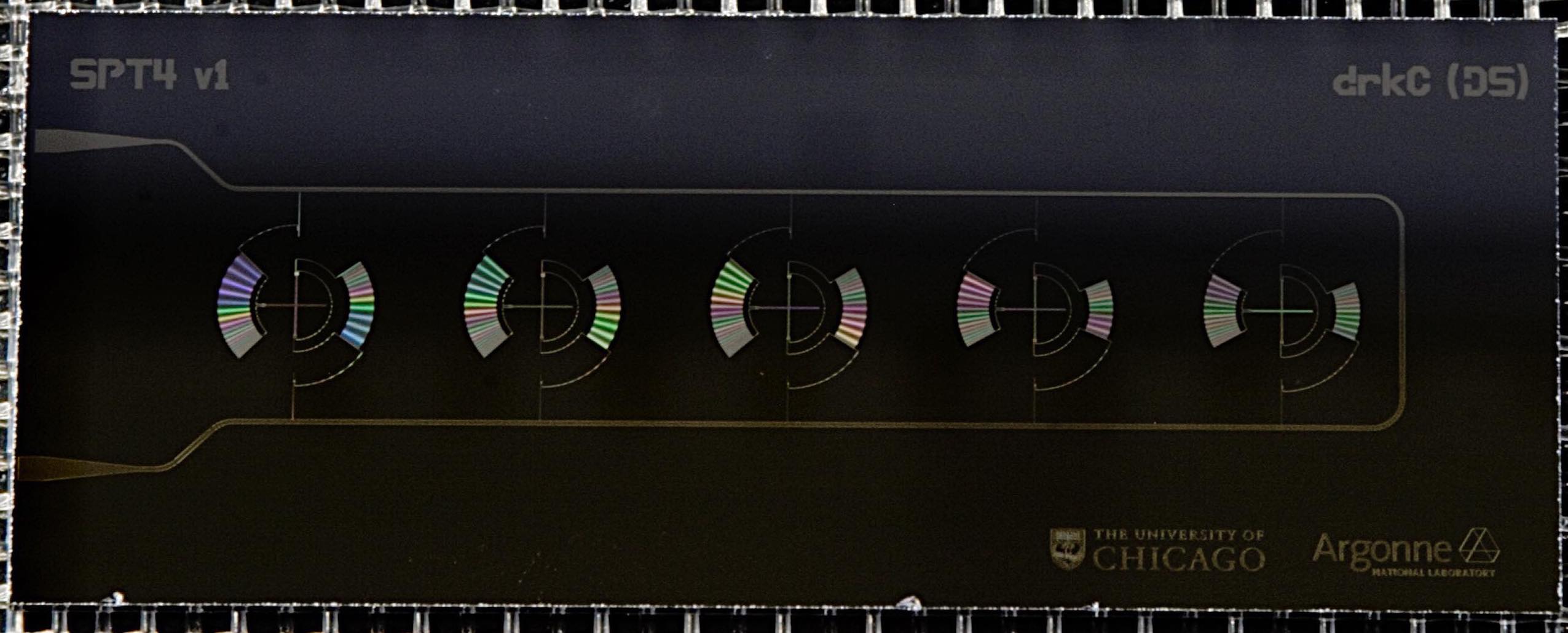
SPT-3G+ will implement MKID arrays with a MUX factor approaching 2k channels per octave, which is a substantial increase over the current SPT-3G TES arrays. As shown in Figure 1, the SPT-3G+ focal plane will be made up of seven single-color optics tubes each illuminating a single 150-mm MKID array. Each of the seven detector modules will contain close to 5k polarization-sensitive detectors, with the full focal plane containing 35k MKIDs in total. This will set new mm-wave MKID detector count and density milestones and will represent the next generation of MKID-based microwave sensing. The ultimate goal of this work will be to demonstrate full science-grade arrays of MKIDs at each SPT-3G+ frequency, which will then be integrated into the SPT-3G+ camera and eventually deployed to the South Pole for on-sky operation. We here present the designs, simulations, and initial test results of detector prototypes for the 220 GHz observing band.
2 Pixel design
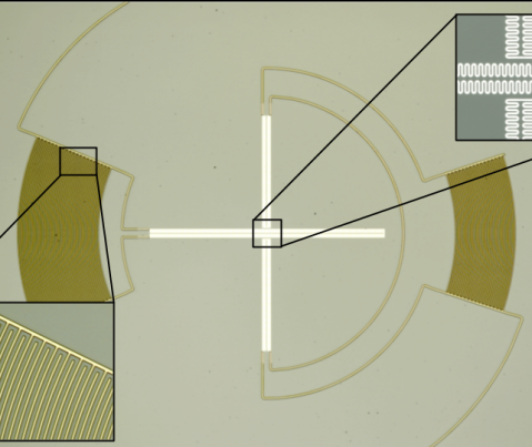
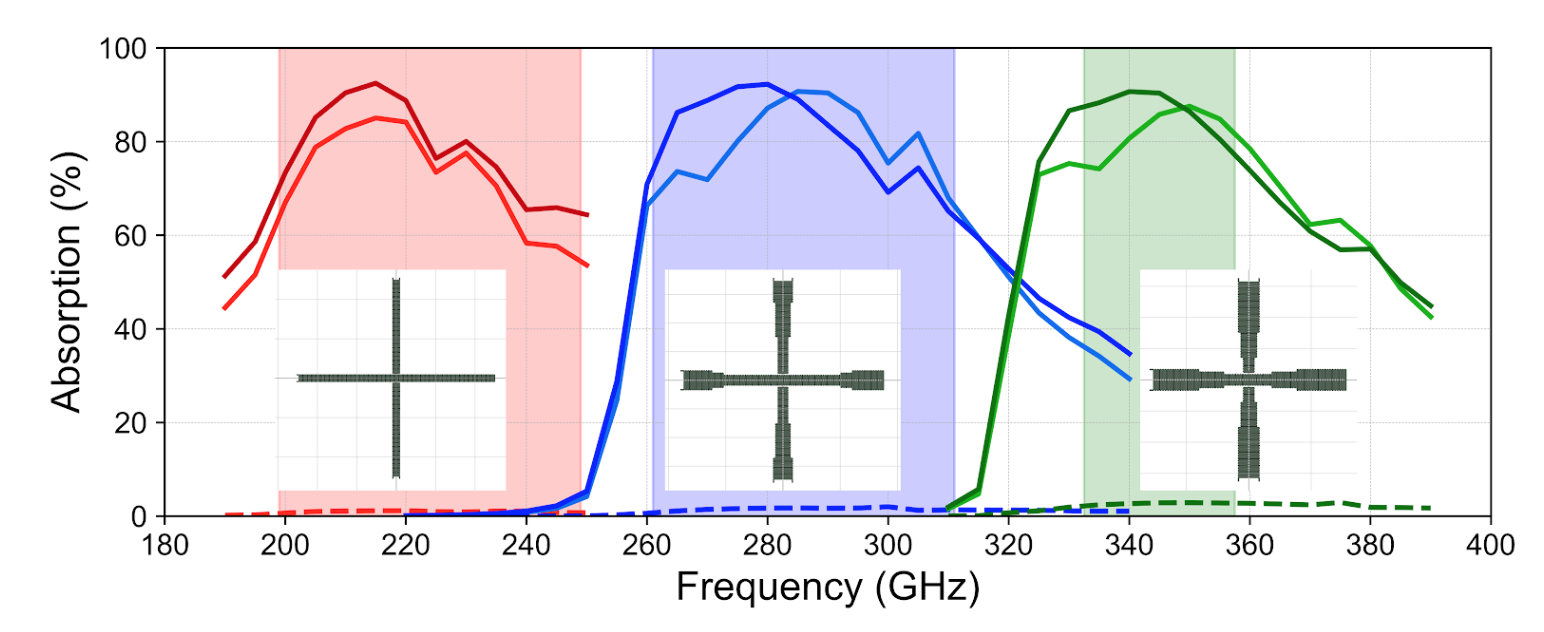
The pixel (shown in the left panel of Figure 2) is composed of two MKIDs aligned with orthogonal polarization modes. This design is based on previous work by [23] and [12] with some important modifications that are necessary for operation at the South Pole. Each MKID consists of an aluminum inductor coupled to a niobium interdigitated capacitor (IDC). The inductor doubles as an impedance-matched optical absorber, where the geometry of the IDC is used to control the resonant frequency of the detector. To maximize the resonator quality factor under the expected optical load, it is necessary to increase the total detector volume while retaining the required responsivity to stay photon-noise dominated. To achieve this, we have introduced meanders into the inductor (see inset of Figure 2) which has the effect of increasing both the volume and absorption efficiency. For higher observing frequencies (and hence smaller waveguides) the meanders increase in width towards the edges of the pixel where the electric field is weaker, allowing for the required increase in absorber volume while minimizing cross-polarization response. The resulting absorber shapes are shown in Figure 3. With these optimized absorber designs, EM simulations indicate that high optical efficiency with low cross-polarization can be achieved (see simulated absorption curves in Figure 3). Simulations indicate a loaded of for all frequency bands, allowing up to 5k channels in the 1-2 GHz readout bandwidth, well above our goal of 2k channels per octave.
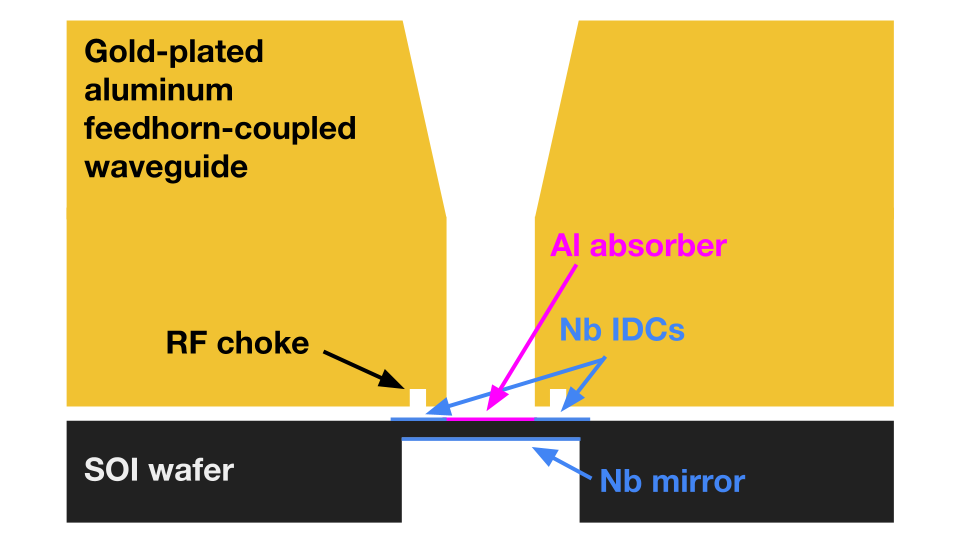
Each pixel is aligned to an aluminum circular waveguide which functions as a high-pass filter, and is encircled by an aluminum RF choke which constrains radiation leakage between adjacent pixels. To set the upper band edge, a metal-mesh low-pass filter is placed in front of a metallic smooth-walled feedhorn that guides radiation into the waveguide. Horn arrays are a well-established method of optical coupling to a MKID, with high efficiency demonstrated up to 1.2 THz [13]. In addition, metallic horn arrays form a natural shield that minimizes inter-pixel optical cross-talk that is known to be an issue for open MKID arrays [25]. The devices are patterned onto a silicon-on-insulator (SoI) wafer with a device layer thickness that is set such that the metallized backside of the wafer functions as an optical backshort. This integrated backshort has a number of advantages in terms of reducing mechanical complexity of the final detector arrays and assembly, as well as enabling post-fabrication adjustment of detector readout frequencies, as discussed in the following section. The waveguide and silicon backshort setup is shown in the right panel of Figure 3.
Figure 2 shows single-pixel and full-chip photographs of a prototype 220 GHz device. The aluminum inductors and niobium IDCs are deposited and patterned via lithography on the front side of a SoI wafer with the necessary device layer thickness. A frontside silicon etch defines the alignment features and dicing lines, and a final backside silicon etch and niobium metallization completes the backshort. Requiring significantly fewer steps than the traditional multi-chroic architectures [10, 19, 22], this process enables rapid design iteration between testing cooldowns. In order to minimize the number of RF readout channels and achieve our goal readout density of 2k/octave, accurate placement of the resonator frequencies is critical. The SPT-3G+ pixel design allows for post-fabrication adjustment of the resonator frequencies by performing a second lithography and trimming a small segment of the IDC. The use of an integrated silicon backshort makes this process possible and is key to maximizing detector yield. The technique has been successfully implemented by a number of groups [20, 18], and recently we have demonstrated the ability to place resonators with a fractional accuracy of [17]. We have also successfully trimmed a prototype device with no loss in resonator yield.
3 Initial test results
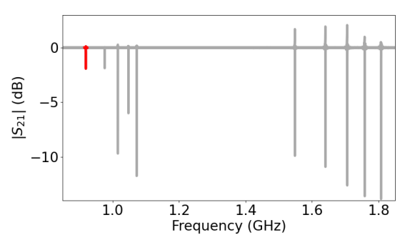
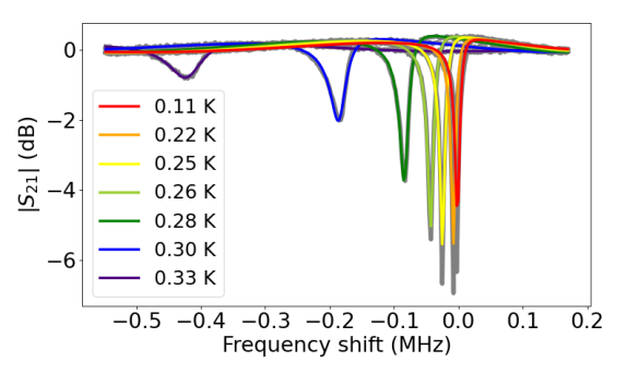
The result of a dark characterization of a chip identical to that pictured in the right-hand panel of Figure 2 is shown in the left-hand panel of Figure 4. The ten resonators present in this chip design appear within the expected readout range, and are located within two banks as intended. The first bank of five contains x-polarization-sensitive resonators, while the second bank contains y-polarization-sensitive resonators. The right-hand panel of Figure 4 shows the response to temperature of the lowest-frequency resonance on this chip (indicated in red in the left-hand panel of Figure 4). As expected, the resonant frequency shifts downward with increasing temperature, and the resonance widens. Lorentzian fits to the data at each temperature (colored lines) indicate inductor quality factors ranging from at 110 mK to at 330 mK. Assuming a 110 mK operating temperature, this agrees with simulations and is well within our target quality factor range, indicating that our ideal 2k/octave multiplexing goal is feasible.
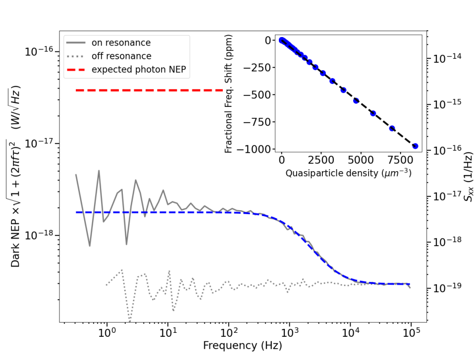
Figure 5 shows the power spectral density () of a series of time ordered data measured for the same resonator at a temperature of 110 mK. We observe the form expected for an MKID that is limited by the generation-recombination noise associated with the superconducting charge carriers [9]. The left axis shows the conversion of this power spectral density to a dark NEP. For a lumped element MKID architecture, this is known to be equivalent to the NEP referenced to absorbed optical power [15]. The dark NEP is estimated from [4] as
| (1) |
where the product in the brackets represents dark responsivity. The term in parentheses is obtained by performing dark sweeps of the resonance at multiple temperatures. The expected quasiparticle density is calculated from each temperature via:
| (2) |
where is the single-spin density of states for aluminum, is the Boltzmann constant, is the temperature of the resonator, and , with K for the aluminum inductor. The critical temperature was extracted from a fit to the resonant frequency shift versus device temperature. Each blue point on the inset to Figure 5 represents the fractional frequency shift of the device in the presence of a given quasiparticle density. The value of is then the magnitude of the slope of the fit to vs . This fit is shown in the inset to Figure 5, and was performed over a high temperature range where the quasiparticle response is dominant. The remaining term in the brackets, from [4], is
| (3) |
where is the expected pair breaking efficiency, is the inductor volume, and s is the quasiparticle lifetime, which is derived from the fit to the dark noise power spectral density rolloff (blue dashed line in Figure 5) at 110 mK. The fit to the noise rolloff here is well represented by a single-pole Lorentzian with time constant , as expected since the the measured quasiparticle lifetime is significantly longer than the resonator ringdown time s.
The red dashed line in Figure 5 represents the expected NEP due to photon noise with 5 pW optical loading, which is the estimated loading at 220 GHz due to atmospheric and instrument emissivity. Within the resonator bandwidth, this photon noise limited NEP is given by
| (4) |
where is the mean photon occupation number and is the best-case detector optical efficiency. This estimate suggests that the intrinsic device noise is well below the expected photon NEP at 220 GHz, and provides strong evidence that this detector design is well suited to achieve the sensitivity requirements of SPT-3G+.
4 Conclusions
We have presented the design for a polarization-sensitive, feedhorn-coupled pixel for use on SPT-3G+, the next-generation focal plane of the South Pole Telescope. We have fabricated prototypes of the 220 GHz design, and have tested these prototypes in a dark environment. Resonator placement and quality factors align with simulations, indicating the feasibility of our 2k/octave multiplexing goal. The dark NEP, calculated assuming a best-case-scenario of 100% optical efficiency, falls well below the theoretical photon NEP at 5 pW of loading, suggesting that background domination is achievable with an optical efficiency above . Optical testing will provide further information on the optical efficiency of these devices, and is currently underway. Further work remains to produce full arrays at all three SPT-3G+ frequencies and to integrate these with the SPT-3G+ cryostat for on-sky deployment.
Acknowledgements.
This material is based upon work supported by the National Science Foundation under NSF-1852617 and NSF-2117894. Work at Argonne National Laboratory was supported by the U.S. Department of Energy (DOE), Office of Science, Office of High Energy Physics, under contract DE-AC02-06CH1137. Partial support was also provided by the DOE Graduate Instrumentation Research Award. This work made use of the Pritzker Nanofabrication Facility of the Institute for Molecular Engineering at the University of Chicago, which receives support from Soft and Hybrid Nanotechnology Experimental (SHyNE) Resource (NSF ECCS-2025633), a node of the National Science Foundation’s National Nanotechnology Coordinated Infrastructure.References
- [1] Marcelo A. Alvarez, Simone Ferraro, J. Colin Hill, Renée Hložek, and Margaret Ikape. Mitigating the optical depth degeneracy using the kinematic sunyaev-zel’dovich effect with cmb-s4 data. Physical Review D, 103(6), Mar 2021.
- [2] J. E. Austermann, et al. Millimeter-Wave Polarimeters Using Kinetic Inductance Detectors for TolTEC and Beyond. Journal of Low Temperature Physics, 193(3-4):120–127, November 2018.
- [3] L. Balkenhol and D. Dutcher, et al. Constraints on CDM Extensions from the SPT-3G 2018 and Power Spectra. arXiv e-prints, page arXiv:2103.13618, March 2021.
- [4] J. Baselmans, S.J.C. Yates, and R. Barends, et al. Noise and sensitivity of aluminum kinetic inductance detectors for sub-mm astronomy. Journal of Low Temperature Physics, 151:524–529, 2008.
- [5] J. J. A. Baselmans, J. Bueno, S. J. C. Yates, O. Yurduseven, N. Llombart, K. Karatsu, A. M. Baryshev, L. Ferrari, A. Endo, D. J. Thoen, P. J. de Visser, R. M. J. Janssen, V. Murugesan, E. F. C. Driessen, G. Coiffard, J. Martin-Pintado, P. Hargrave, and M. Griffin. A kilo-pixel imaging system for future space based far-infrared observatories using microwave kinetic inductance detectors. Astronomy and Astrophysics, 601:A89, May 2017.
- [6] B. A. Benson et al. SPT-3G: a next-generation cosmic microwave background polarization experiment on the South Pole telescope, volume 9153 of Society of Photo-Optical Instrumentation Engineers (SPIE) Conference Series, page 91531P. 2014.
- [7] Benjamin Beringue, P. Daniel Meerburg, Joel Meyers, and Nicholas Battaglia. Cosmology with Rayleigh scattering of the cosmic microwave background. JCAP, 2021(1):060, January 2021.
- [8] A. D’Addabbo et al. The NIKA instrument: results and perspectives towards a permanent KID based camera for the Pico Veleta observatory. arXiv e-prints, page arXiv:1312.4801, December 2013.
- [9] P. J. de Visser, J. J. A. Baselmans, P. Diener, S. J. C. Yates, A. Endo, and T. M. Klapwijk. Generation-Recombination Noise: The Fundamental Sensitivity Limit for Kinetic Inductance Detectors. Journal of Low Temperature Physics, 167(3):335–340, May 2012.
- [10] S. M. Duff, J. Austermann, J. A. Beall, D. Becker, R. Datta, P. A. Gallardo, S. W. Henderson, G. C. Hilton, S. P. Ho, J. Hubmayr, B. J. Koopman, D. Li, J. McMahon, F. Nati, M. D. Niemack, C. G. Pappas, M. Salatino, B. L. Schmitt, S. M. Simon, S. T. Staggs, J. R. Stevens, J. Van Lanen, E. M. Vavagiakis, J. T. Ward, and E. J. Wollack. Advanced ACTPol Multichroic Polarimeter Array Fabrication Process for 150 mm Wafers. Journal of Low Temperature Physics, 184(3):634–641, August 2016.
- [11] D. Dutcher and L. Balkenhol et al. Measurements of the E-Mode Polarization and Temperature-E-Mode Correlation of the CMB from SPT-3G 2018 Data. arXiv e-prints, page arXiv:2101.01684, January 2021.
- [12] Nicholas Galitzki et al. The Next Generation BLAST Experiment. Journal of Astronomical Instrumentation, 3(2):1440001, November 2014.
- [13] Christopher E. Groppi, P. M. Mauskopf, P. A. R. Ade, and M. Underhill. Design and measurement of a direct-drillable smooth walled feedhorn at 1.2 THz for the next generation BLASTPol experiment. In Wayne S. Holland and Jonas Zmuidzinas, editors, Millimeter, Submillimeter, and Far-Infrared Detectors and Instrumentation for Astronomy VIII, volume 9914, pages 645 – 650. International Society for Optics and Photonics, SPIE, 2016.
- [14] S. Guns, et al. Detection of Galactic and Extragalactic Millimeter-Wavelength Transient Sources with SPT-3G. arXiv e-prints, page arXiv:2103.06166, March 2021.
- [15] R. M. J. Janssen, A. Endo, P. J. de Visser, T. M. Klapwijk, and J. J. A. Baselmans. Equivalence of optical and electrical noise equivalent power of hybrid NbTiN-Al microwave kinetic inductance detectors. Applied Physics Letters, 105(19):193504, November 2014.
- [16] Antony Lewis. Rayleigh scattering: blue sky thinking for future cmb observations. Journal of Cosmology and Astroparticle Physics, 2013(08):053–053, Aug 2013.
- [17] R. McGeehan, P. S. Barry, E. Shirokoff, C. M. Bradford, G. Che, J. Glenn, S. Gordon, S. Hailey-Dunsheath, M. Hollister, A. Kovács, H. G. LeDuc, P. Mauskopf, C. McKenney, T. Reck, J. Redford, C. Tucker, J. Turner, S. Walker, J. Wheeler, and J. Zmuidzinas. Low-Temperature Noise Performance of SuperSpec and Other Developments on the Path to Deployment. Journal of Low Temperature Physics, 193(5):1024–1032, December 2018.
- [18] Christopher M. McKenney, Jason E. Austermann, James A. Beall, Bradley J. Dober, Shannon M. Duff, Jiansong Gao, Gene C. Hilton, Johannes Hubmayr, Dale Li, Joel N. Ullom, Jeff L. Van Lanen, and Michael R. Vissers. Tile-and-trim micro-resonator array fabrication optimized for high multiplexing factors. Review of Scientific Instruments, 90(2):023908, February 2019.
- [19] C. M. Posada, et al. Fabrication of Detector Arrays for the SPT-3G Receiver. Journal of Low Temperature Physics, 193:703–711, December 2018.
- [20] S. Shu, M. Calvo, J. Goupy, S. Leclercq, A. Catalano, A. Bideaud, A. Monfardini, and E. F. C. Driessen. Increased multiplexing of superconducting microresonator arrays by post-characterization adaptation of the on-chip capacitors. Applied Physics Letters, 113(8):082603, August 2018.
- [21] Kendrick M. Smith and Simone Ferraro. Detecting patchy reionization in the cosmic microwave background. Phys. Rev. Lett., 119:021301, Jul 2017.
- [22] Q. Y. Tang, P. S. Barry, T. W. Cecil, and E. Shirokoff. Fabrication of OMT-Coupled Kinetic Inductance Detector for CMB Detection. Journal of Low Temperature Physics, 199:362–368, January 2020.
- [23] M. R. Vissers, J. E. Austermann, M. Malnou, C. M. McKenney, B. Dober, J. Hubmayr, G. C. Hilton, J. N. Ullom, and J. Gao. Ultrastable millimeter-wave kinetic inductance detectors. Applied Physics Letters, 116(3):032601, January 2020.
- [24] M. R. Vissers, J. Gao, D. S. Wisbey, D. A. Hite, C. C. Tsuei, A. D. Corcoles, M. Steffen, and D. P. Pappas. Low loss superconducting titanium nitride coplanar waveguide resonators. Applied Physics Letters, 97(23):232509, 2010.
- [25] Stephen J. C. Yates, Simon Doyle, Peter Barry, Andrey M. Baryshev, Juan Bueno, Lorenza Ferrari, Nuria Llombart, Vignesh Murugesan, David J. Thoen, Ozan Yurduseven, and Jochem J. A. Baselmans. Eliminating stray radiation inside large area imaging arrays. In Millimeter, Submillimeter, and Far-Infrared Detectors and Instrumentation for Astronomy IX, volume 10708, page 107081X. International Society for Optics and Photonics, July 2018.
Data availability statement: The datasets generated during and/or analyzed during the current study are available from the corresponding author on reasonable request.