1: School of Physics & Astronomy, Cardiff University, Cardiff CF24 3AA, UK
2: Kavli Institute for Cosmological Physics, University of Chicago, Chicago, IL 60637, USA
3: Fermi National Accelerator Laboratory, Batavia, IL 60510, USA
4: High-Energy Physics Division, Argonne National Laboratory, Lemont, IL 60439, USA
The Simulation and Design of an On-Chip Superconducting Millimetre Filter-Bank Spectrometer
Abstract
Superconducting on-chip filter-banks provide a scalable, space saving solution to create imaging spectrometers at millimetre and sub-millimetre wavelengths. We present an easy to realise, lithographed superconducting filter design with a high tolerance to fabrication error. Using a capacitively coupled microstrip resonator to define a narrow () spectral pass band, the filtered output of a given spectrometer channel directly connects to a lumped element kinetic inductance detector. We show the tolerance analysis of our design, demonstrating change in filter quality factor to any one realistic fabrication error and a full filter-bank efficiency forecast to be 50% after accounting for fabrication errors and dielectric loss tangent.
Keywords:
Millimeter-wave, Spectrometry, On-Chip Filter-Bank, Superconductivity1 Introduction
Millimetre wavelength astronomy contains a wealth of largely untapped information about the universe, ranging from measurements of the cosmic microwave background, to high redshift sources, to the inner workings of the dust-enshrouded regions of space. In the millimetre range, current, conventional spectrometer technology cannot scale up effectively to meet the sensitivity requirements for next-generation science cases. However, by capitalising on the small energy gap of superconductors, high sensitivity, and ease of microwave circuit integration, superconducting filter-bank spectrometers (FBS) will be central in a range of future surveys in the millimetre region of the spectrum.
FBS make use of the low-loss properties of superconductors operating well below the superconducting critical temperature (), integrated microwave circuitry, and the sensitive and multiplexing capabilities of kinetic inductance detectors (KIDs) to create an efficient, compact, and sensitive spectrometer that does not need large dispersive optical components, complex readout systems, or noise limiting amplifiers and local oscillators.
This paper presents a novel filter geometry with the application tailored to a medium-resolution mm-wave FBS, which to date has been demonstrated in two alternative instruments [1, 2]. This FBS is motivated by the SPT-SLIM project which is discussed in more detail in [3, 4]. Each filter-bank will consist of 200 filter channels with a spectral resolution of covering the mm atmospheric transmission window (GHz - GHz).
2 On-Chip Filter-Bank Spectrometer Design
Incident light is coupled onto a transmission line via an antenna and guided to the filter-bank. The filter-bank is made up of a series of capacitively-coupled half-wave () resonators each with a different resonant frequency, , set by the length, and spectral bandwidth, , set by the coupling to the feedline.
The two key performance metrics of an on-chip spectrometer are the spectral resolution and the filter efficiency. The resolution, , is equivalent to the quality factor, , of each filter channel’s resonator,
| (1) |
The filter efficiency is defined as the ratio of the total signal output through the channels to that coupled to the FBS. The maximum power transferred through the filter to the detector that can be achieved for a feedline-filter T-junction such as this is 50% of the incident signal. Note that this is only the limit for a single filter; the overall FBS efficiency can exceed this with over-sampled filters [5].
3 Filter Geometry
The device will be built from a silicon on oxide (SOI) substrate (see Fig. 1) due to requirements for the architecture of the orthomode transducer (OMT) antennas and detectors. For further details see [4]. Niobium is used for the feedline and filter structure since it is nearly lossless for the range of operation, due to its large superconducting gap.
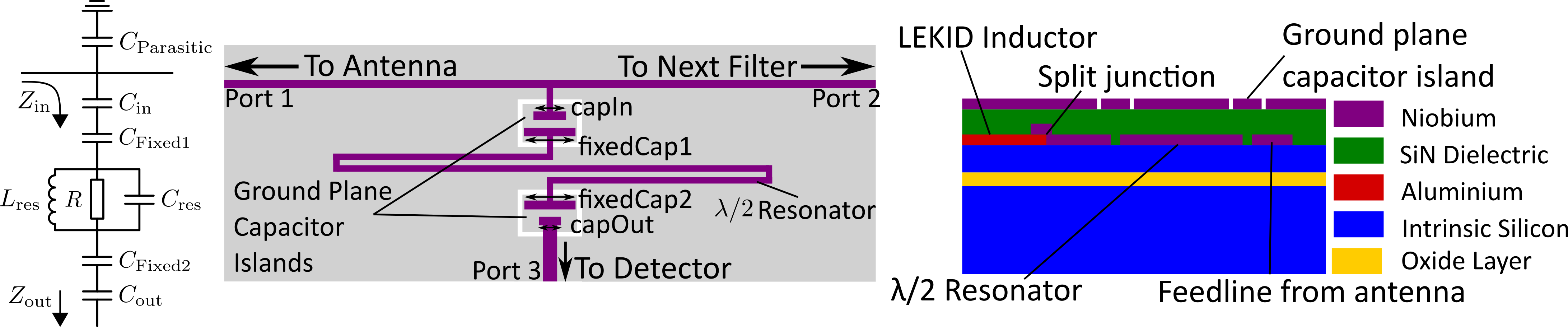
A filter channel is created by coupling a resonator to the main filter-bank feedline. On resonance, the current distribution results in a current node at each end of the resonator. This enables two coupling methods: inductively, by exploiting the current maximum in the centre as demonstrated by SuperSpec [1, 6]; or capacitively, using the voltage maximum at the ends, as seen in the DESHIMA [2, 7] device. Both examples tune the coupling quality factors, , via the separation between feedline and resonator. Due to fabrication tolerances, the tuning precision of is somewhat limited for such proximity couplings. We present an alternative coupling scheme that uses a pseudo-lumped element capacitor island in the ground plane to form parallel plate capacitors; two at either end of the resonator, as shown in Fig. 1. This allows for a highly tuneable capacitive coupling using a microstrip architecture to minimize losses due to radiation [8].
The spectral resolution of a single channel can be written as the inverse sum of the quality factors due to losses within resonator, , the coupling to the feedline, , and detector coupling, , [1],
| (2) |
and can be controlled by changing the overlapping surface area of the parallel plates. For this design, is largely controlled by the capacitor widths “capIn” and “capOut” (see Fig. and by the resonator length (see Fig. 1). Using Sonnet EM [9] to simulate the geometry in Fig. 1, for a variety of resonator lengths across the band, a simulation sweeping capIn values was carried out with the port 3 impedance set high enough to resemble an open circuit. Fitting Lorentzian curves, the capIn yielding a can be interpolated. This value is then used whilst sweeping capOut with a matched load at port 3 to obtain the capOut value giving a peak value of 0.5 in the . This should ideally be when , yet this is not quite the case since the inability to fully de-embed the port 3 output line limits the complete removal of the contribution to of capOut when optimising capIn. This data was used to build an interpolation table that yields the required geometry needed for a filter with any desired f0.
There is a small section of microstrip between the feedline and “capIn”, which, off-resonance acts as a very short stub, which is well modelled as a parasitic capacitance to ground. An effect analogous to the impedance engineering in superconducting parametric amplifiers [10] occurs when multiple small mismatches are present along the feedline. From our simulations, to prevent the resulting stopband entering into the operational frequency band, the electrical length between filters must be suitably small () compared to the smallest half wavelength in the band.
4 Loss Tangent Impact
The presence of a dielectric layer introduces a loss mechanism due to parasitic two level systems (TLS), which has been extensively studied [11, 12]. The dielectric loss tangent, , is a measure of the energy dissipated through this mechanism and hence can be expressed as a quality factor and is considered to be the dominant contribution to in Eq. 2 thus, . Whilst there are limited published results for the loss tangent of SiN, those that are found in the literature are measured at microwave frequencies below [13, 14] and require a rough extrapolation of the frequency dependence up to the relevant frequencies for mm-wave astronomy. Moreover, the dielectric tan varies considerably depending on the deposition system and process, thus it will be crucial to characterise our SiN tan. For this study, we assume a SiN dielectric tan of [15], since this is similar in process and device architecture.
When optimised, the maximal fraction of power, that passes through the filter and terminates at the detector (filter efficiency) depends on the ratio of to as [6]
| (3) |
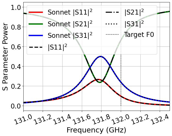
Fig. 2 shows the impact on that the loss tangent has over a range of predicted by Eq. 3, as well as a Sonnet simulation corrected for the effective dielectric constant, which shows good agreement with a filter at GHz. There is also the expected trade off between and for a given dielectric tan, and Fig. 2 clearly show what stands to be gained from lower loss dielectrics such as as is expected from amorphous silicon [2].

5 Fabrication Error Tolerance
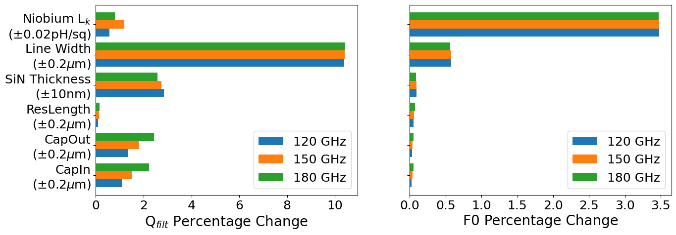
The largest source for disagreement between simulated and fabricated filters is generally due to fabrication error, a somewhat unavoidable aspect of micro-fabrication. Deviations in the kinetic inductance, , of the superconducting film, the dielectric thickness/constant, and over or under etching, have all been shown to have a considerable impact on the filter properties, and this is particularly the case for etch sensitivity with proximity-coupled filters [16]. Therefore it is necessary to understand the tolerance of a design to a variety of fabrication errors. Fig. 3 shows the filters’ and sensitivity to variations in key features of our architecture using the python model described in Sec. 6, to study the impact of typical deposition and lithography error based on unoptimised fabrication runs at Cardiff.
These results clearly demonstrate that this design has a high tolerance to fabrication error, particularly given that worst case errors were used. The resonant frequency is most sensitive to variations in , however this is only approximately and suitably constant across the band. Thus, all filters should shift by the same amount. Note, changes in due to a variation in niobium thickness were not considered as for niobium is expected to vary slowly with thickness for nm thick niobium with a magnetic penetration depth of nm. Furthermore, we see a promising forecast for the tolerance of the geometry to the variables that are the main controllers of , namely “CapIn”, “CapOut”, and “SiN Thickness” since these control the capacitance of the coupling capacitors, each resulting in a shift in Q between 2-3%. By comparison, proximity-coupled filters demonstrate a far higher sensitivity to etch error at the coupling geometry where a change in can triple the value of [16]. This low tolerance removes the need to use electron beam lithography, a more precise but time-consuming etching method, reducing the cost, and speed of device turn around.
6 Filter-Bank Performance
Sonnet EM captures electromagnetic behaviour otherwise overlooked by lumped-element simulation software. This is at the cost of simulation run time, and therefore unsuitable for simulating the performance of an FBS with more than three filters. Furthermore, niche issues start to become a problem such as larger box sizes result in dimensions that are a similar size to the signal wavelength creating interfering box modes.
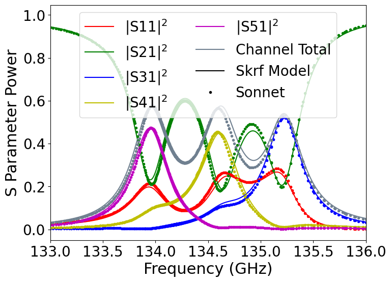
We have developed a Python model based on scikit-rf, an open source module to create a series of cascaded lumped-element networks connected by transmission lines to simulate an N-channel filterbank. Similar methods have already been developed to simulate and analyse FBSs [17] but only from the perspective of resonator parameters, rather than using physical properties as the simulation handles, such as geometry dimensions and dielectric thickness. The model produces similar microwave responses to Sonnet by extracting the microwave component and material properties from small scale Sonnet simulations to produce libraries for use across full, cascaded simulations. For example, the coupling capacitors were modelled as a lumped capacitance with parasitic series lumped inductances on either side with values calibrated against Sonnet simulations. A single filter typically taking 10 minutes to simulate in Sonnet can be simulated in 5 seconds. The agreement between Sonnet simulations and the python model can be seen in Fig. 4. This code enabled the tolerance analysis shown in Section 5, and allowed us to qualitatively observe the impact the fabrication errors have on the spectral response when errors are considered across multiple interacting (over-sampled) channels.
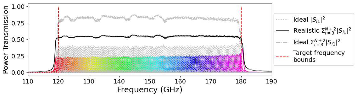
An example of the full FBS can be seen in Fig. 5. The impact of these fabrication errors is minor compared to that of tan, which accounts for much of the difference between the ideal and realistic FBS, displaying a large change in as expected from the results seen in Section 4. Despite this, the FBS should still exhibit 50%.
7 Conclusion
We have presented a new filter design for a superconducting microstrip FBS and presented the optimisation process and the tolerance analysis of the design for a variety of key fabrication errors. The main differences in design compared to other FBSs [1, 2] include: the use of microstrip transmission line reducing loss by radiation loss, and parallel plate capacitor couplers at the end of each resonator rather than proximity coupling. Whilst also being a simple and easy to realise design, simulations show these filters have a high tolerance to fabrication error. The quality factor of each filter is most sensitive to variations in microstrip line widths (smallest width: 2m) due to over or under etching, resulting in a worst case shift in of for a pessimistic etch uncertainty of . The resonant frequency of each filter is also suitably robust, with the largest shift in of being due to a deviation in the niobium kinetic inductance.
A python model, calibrated with Sonnet simulations was used to simulate the FBS and study the impact of fabrication errors on the spectral response. These simulations imply there will be limited impact on the FBS performance with a smoothly varying etch error and dielectric thickness over the wafer. Instead, improving the dielectric loss tangent is the aspect of the filter bank design that will yield the greatest improvements in optical efficiency. For example, the lossless FBS could achieve , whereas with the expected SiN tan, we see this reduce to just under 50% in the best case.
Acknowledgements.
This work was supported by the members of the SPT-SLIM collaboration and made use of scikit-rf, an open-source Python package for RF and Microwave applications. G. Robson acknowledges the continuing support from the Science and Technology Facilities Council Ph.D studentship programme under grant reference ST/S00033X/1. We thank the reviewers who have provided insightful comments leading to improvements to this paper. The datasets generated during and/or analysed during the current study are available from the corresponding author on reasonable request.References
- [1] S. Hailey-Dunsheath, E. Shirokoff, P. S. Barry, C. M. Bradford, G. Chattopadhyay, P. Day, S. Doyle, M. Hollister, A. Kovacs, H. G. LeDuc, P. Mauskopf, C. M. McKenney, R. Monroe, R. O’Brient, S. Padin, T. Reck, L. Swenson, C. E. Tucker, J. Zmuidzinas, Proc. SPIE 9153 (2014). DOI: 10.1117/12.2057229.
- [2] A. Endo, K. Karatsu, Y. Tamura, T. Oshima, A. Taniguchi, T. Takekoshi, S. Asayama, T. J. L. C. Bakx, S. Bosma, J. Bueno, K. W. Chin, Y. Fujii, K. Fujita, R. Huiting, S. Ikarashi, T. Ishida, S. Ishii, R. Kawabe, T. M. Klapwijk, K. Kohno, A. Kouchi, N. Llombart, J. Maekawa, V. Murugesan, S. Nakatsubo, M. Naruse, K. Ohtawara, A. P. Laguna, J. Suzuki, K. Suzuki, D. J. Thoen, T. Tsukagoshi, T. Ueda, P. J. de Visser, P. P. van der Werf, S. J. C. Yates, Y. Yoshimura, O. Yurduseven, J. J. A. Baselmans, Nat Astron 3, 989–996 (2019). DOI: 10.1038/s41550-019-0850-8.
- [3] K. S. Karkare, J. Low Temp. Phys This Special Issue (2021).
- [4] P. S. Barry, J. Low Temp. Phys This Special Issue (2021).
- [5] A. Kovács, P. S. Barry, C. M. Bradford, G. Chattopadhyay, P. Day, S. Doyle, S. Hailey-Dunsheath, M. Hollister, C. McKenney, H. G. LeDuc, N. Llombart, D. P. Marrone, P. Mauskopf, R. C. O’Brient, S. Padin, L. J. Swenson, and J. Zmuidzinas, Proc. SPIE 8452 (2012). DOI: 10.1117/12.927160.
- [6] E. Shirokoff, P. S. Barry, C. M. Bradford, G. Chattopadhyay, P. Day, S. Doyle, S. Hailey-Dunsheath, M. I. Hollister, A. Kovács, C. McKenney, H. G. Leduc, N. Llombart, D. P. Marrone, P. Mauskopf, R. O’Brient, S. Padin, T. Reck, L. J. Swenson, J. Zmuidzinas, Proc. SPIE 8452 (2012). DOI: 10.1117/12.927070.
- [7] A. Endo, C. Sfiligoj, S. J. C. Yates, J. J. A. Baselmans, D. J. Thoen, S. M. H. Javadzadeh, P. P. van der Werf, A. M. Baryshev, and T. M. Klapwijk, Appl. Phys. Lett. 103, 032601 (2013). DOI: 10.1063/1.4813816.
- [8] A. Endo, K. Karatsu, A. P. Laguna, B. Mirzaei, R. Huiting, D. Thoen, V. Murugesan, S. J. C. Yates, J. Bueno, N. V. Marrewijk, S. Bosma, O. Yurduseven, N. Llombart, J. Suzuki, M. Naruse, P. J. de Visser, P. P. van der Werf, T. M. Klapwijk, J. J. A. Baselmans, J. Astron. Telesc. Instrum. Syst. 5 (3) 035004 (2019). DOI: 10.1117/1.JATIS.5.3.035004.
- [9] Sonnet Suites, Version 17.56. Accessed 2021. Available: www.sonnetsoftware.com
- [10] B. H. Eom, P. K. Day, H. G. LeDuc, and J. Zmuidzinas. Nat. Phys. 8, 623-627 (2012). DOI: 10.1038/nphys2356
- [11] J. Gao, 2008, PhD Thesis, Department of Physics, Caltech, Pasadena, CA, USA.
- [12] D. P. Pappas, M. R. Vissers, D. S. Wisbey, J. S. Kline, J. Gao, in IEEE Transactions on Applied Superconductivity, vol. 21, no. 3, pp. 871-874, (2011), DOI: 10.1109/TASC.2010.2097578.
- [13] J. M. Martinis, K. B. Cooper, R. McDermott, M. Steffen, M. Ansmann, K. D. Osborn, K. Cicak, Se. Oh, D. P. Pappas, R. W. Simmonds, and C. C. Yu Phys. Rev. Lett. 95, 210503 (2005), DOI: 10.1103/PhysRevLett.95.210503.
- [14] H. Paika, K. D. Osborn, Appl. Phys. Lett. 96, 072505 (2010), DOI: 10.1063/1.3309703.
- [15] S. Hailey-Dunsheath, P. S. Barry, C. M. Bradford, G. Chattopadhyay, P. Day, S. Doyle, M. Hollister, A. Kovacs, H. G. LeDuc, N. Llombart, P. Mauskopf, C. McKenney, R. Monroe, H. T. Nguyen, R. O’Brient, S. Padin, T. Reck, E. Shirokoff, L. Swenson, C. E. Tucker, J. Zmuidzinas, J. Low Temp. Phys. 176, 841–847 (2014). DOI: 10.1007/s10909-013-1068-2.
- [16] A. P. Laguna, K. Karatsu, D. Thoen, V. Murugesan, B. Buijtendorp, A. Endo, J. Baselmans, in IEEE Transactions on Terahertz Science and Technology, (2021) DOI: 10.1109/TTHZ.2021.3095429.
- [17] G. Che, 2018 PhD Thesis, Department of Physics, Arizona State University, Tucson, AZ, USA.