Microstructure and the Boson-peak in thermally-treated InO films
Abstract
We report on the correlation between the boson-peak and structural changes associated with thermally-treating amorphous indium-oxide films. In this process, the resistance of a given sample may decrease by a considerable margin while its amorphous structure is preserved. In the present study, we focus on the changes that result from the heat-treatment by employing electron-microscopy, X-ray, and Raman spectroscopy. These techniques were used on films with different stoichiometry and thus different carrier-concentration. The main effect of heat-treatment is material densification, which presumably results from elimination of micro-voids. The densified system presents better wavefunction-overlap and more efficient connectivity for the current flow. X-ray, and electron-beam diffraction experiments indicate that the heat-treated samples show significantly less spatial heterogeneity with only a moderate change of the radial-distribution function metrics. These results are consistent with the changes that occur in the boson-peak characteristics due to annealing as observed in their Raman spectra.
I Introduction
Disorder plays a major role in the properties of solids. The study of disorder is a challenge in terms of being able to control, characterize, and quantify it. A significant effort in this vein was invested in the field of electronic transport. In particular, the need for modifying and quantifying disorder is an essential ingredient in the field of disorder-induced phenomena. Prime examples in this category are the metal-insulator transition and the superconductor-insulator transition. The system resistivity is sometimes used as an empirical measure of disorder in these studies. Electric conductivity of a solid is arguably its most sensitive property and it may be affected by different means, not all of them may be attributed to disorder. A change in carrier-concentration for example, naturally affects conductivity while only a small (and indirect) change in disorder may be incurred in the process.
Restricting the lateral dimensions of the sample has been widely used to increase scattering. This is in particular a viable technique to change disorder in transport studies of thin films. However to introduce strong disorder in a three-dimensional system one may have to resort to alloying or use a two-component mixture; a granular system. An effective method that was employed to introduce disorder in a metallic system was exposure to neutron or -particle radiation. This technique was employed in modifying the transport properties of A-15, MgB, and other materials by introducing point-defects and grain-boundary spacing 1 .
A complementary, backward procedure is thermal-annealing. This is an effective way to reduce disorder when the system is disordered to start with, a common situation in vacuum deposited or quench-cooled systems. Thermal-annealing has been successfully used in various transport experiments as a means of fine-tuning the disorder of amorphous indium-oxide (InO) films. It has been shown that thermally-treating InO films may result in resistance change of up to 4-5 orders of magnitude at room-temperature with only a small change of carrier-concentration measured by the Hall effect. It seems therefore that the huge change in resistance is due to enhanced mobility, suggestive of a less disordered system. The range of disorder attainable with this method allows studies of both sides of the metal-insulator, and the superconductor-insulator transitions of this material. It was argued that the main reason for the resistance change is densification 2 . This was supported by demonstrating the similarity of the change in the optical-gap during thermally-annealing InO films, and in studies of pressure-induced densification of glasses.
Another property known to be sensitive to disorder in solids is the boson-peak (BP), which has been widely studied in amorphous systems and glasses 3 ; 4 ; 5 ; 6 ; 7 ; 8 ; 9 ; 10 ; 11 ; 12 . The BP is a feature that appears at the low energy vibrational-density-of-states of amorphous and disordered systems. This feature may be resolved by heat-capacity, neutron scattering experiments, and by Raman spectroscopy. There are several competing theoretical models that purport to account for the mechanism that underlies the BP. The common ingredient in the great majority of them is spatial disorder 4 ; 5 ; 8 ; 13 ; 14 ; 15 ; 16 . This makes the characteristics of the BP a relevant probe for monitoring changes in disorder. This is of particular relevance for amorphous systems where quantifying disorder is a challenge. In addition to the lack of long-range order, most amorphous solids exhibit mass density that is lower than their crystalline counterpart. This is presumably due to their being formed by fast cooling from the liquid or gaseous phase 17 . The latter preparation method, quench-cooling the material from the vapor phase onto a cold substrate, usually results in a porous structure that has many micro-voids reducing the material bulk specific gravity. Consequently, an appreciable volume change may be affected in these structures upon application of pressure, and by thermal-treatment 2 .
In this work we attempt to further elucidate these issues using several versions of amorphous indium-oxide as a model system for a metallic glass. This allows us to track changes in the BP due to quantifiable changes of disorder. Raman spectroscopy taken from as-made and annealed InO films of different composition, reveal significant changes in the BP magnitude and shape. It is noted that Raman spectroscopy may not faithfully convey the detailed shape of the BP as compared with, for example, heat capacity measurements 18 . However, it is still a viable tool to identify relative changes in the spectra caused by modification of the system structure. Our Raman spectra results are discussed in conjunction with the microstructure information based on X-ray and electron-diffraction experiments made on these samples. In particular, our study illustrates how various aspects of structural disorder affect electronic properties such as conductivity as compared with their effect on the BP shape and magnitude. The similarities and differences with the behavior of the BP in other glasses were pressure was used to modify the structure are pointed out.
II Experimental
II.1 Samples preparation and characterization
The InO films were e-gun evaporated onto room-temperature substrates using 99.999% pure InO sputtering-target. Deposition was carried out at the ambience of 30.5x10 to 40.5x10 Torr oxygen-pressure maintained by leaking 99.9% pure O through a needle valve into the vacuum chamber (base pressure 10 Torr). Different substrates were used for the samples prepared for the different measurements techniques. Undoped silicon wafers were used as substrates for electrical measurements, X-ray diffraction (XRD) and Raman spectroscopy measurements. Carbon-coated copper grids were used for transmission electron microscopy (TEM) imaging and electron-diffraction. During deposition and thermal-treatment the grids were anchored to glass-slides by small indium balls pressed onto the glass. The deposited film on the rest of the slide was used for monitoring the sample resistance. X-ray reflectometry (XRR) measurements were performed on samples deposited on 3.8 mm thick float-glass-slides.
Rates of deposition in the range 0.3-2.5 Å/s were used to produce films with different compositions; The InO samples had carrier-concentration N that increases with the ratio of deposition-rate to the oxygen-partial-pressure. For the rates-pressures used here N was in the range 2x10cm to 5x10cm as measured by Hall effect at room-temperature using a Hall-bar control-sample prepared simultaneously for each sample deposition. The evaporation source to substrate distance in the deposition chamber was 451cm. This yielded films with thickness uniformity of 2% across a 2x2cm area. Lateral sizes of samples used for transport measurements was typically 1x2mm (width x length respectively), and 1x1cm for the Raman spectroscopy. To afford reasonable resolution for electron-microscopy thickness of the films used for TEM work was typically d=20010 Å.
Three batches of InO with different carrier-concentrations N=(41)x10cm, (10.5)x10cm, and (91)x10cm were used for Raman spectroscopy. For structural analysis we used films characterized by the Ioffe-Regel parameter k=(3) in the range of 0.08 to 0.4. Here is the room-temperature conductivity. This range covers the critical-value of k=0.320.2 where the metal-insulator transition and superconductor-insulator transition of InO take place 19 ; 20 .
High resolution TEM images and electron diffraction patterns were taken with the Philips Tecnai F20 G2 operating at 200kV. X-ray diffraction and reflectometry were taken with Bruker diffractometer AXS D8 Advance equipped with Lynexeye XE-T silicon strip-detector. The diffractometer has step resolution of 10deg.
Raman spectroscopy at Ben-Gurion University of the Negev was performed with a home-built ultra-low frequency Raman microscope confocal system that was assembled and optimized for measurements down to 10cm. The setup employed a single longitudinal mode green-laser operating at 532nm. The laser power used in the measurements was typically 3mW for a spot diameter of 2.6m. The scattered signal was collected via high throughput 532 longpass nano-edge filters and a single spectrometer 21 . Complementary Raman spectroscopy studies in the Hebrew University were taken with a Renishaw inVia Reflex Spectrometer using a laser beam with either 514 nm or 785 nm wavelength and edge-filter at 70cm therefore these measurements were limited to energies 80cm.
II.2 The thermal-treatment protocol
The protocol we routinely use for monitoring the annealing process involves the following steps: After removal from the deposition chamber, the sample was mounted onto a heat-stage in a small vacuum-cell wired to make contacts with the sample for electrical measurements, and a thermocouple attached to the sample-stage as a thermometer. Resistance measurements were performed by a two-terminal technique using either the computer-controlled HP34410A multimeter or the Keithley K617. Next the heating stage is energized, and the resistance and temperature is continuously measured throughout the heating, relaxation, and cooling periods. A typical annealing cycle is illustrated in figure 1:
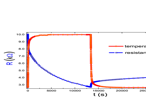
The sharp changes in the sample resistance R when the heating is turned on and off are mostly due to the temperature dependent coefficient that in this disorder regime is negative. However, during the time that the temperature has settled at the target value for annealing, R continues to slowly decrease. Then, after cooldown to room-temperature, the resistance slowly increases approaching an asymptotic value that, ordinarily, is smaller than at the start of the heat-treatment cycle.
These slow R(t) reflect changes in the system volume (densification and rarefaction respectively). The change in volume in the process of thermally-treating InO films was demonstrated in an interference experiment using grazing-angle X-ray technique 22 . It was further correlated with in-situ resistivity and optical-spectroscopy measurements 22 . For InO, a system with the Fermi energy in the conduction band, higher density typically yields higher mobility. This may be due to the enhanced overlap of wavefunctions and improved connectivity. It will be shown below that there is more to the improved mobility than just densification.
The time-dependent processes that occur while the temperature is constant were qualitatively accounted for by a heuristic model based on the two-level-systems that make up the potential landscape of the disordered system 23 . A similar approach was used in 24 to offer a platform for accounting for thermal expansion of glasses.
III Results and discussion
III.1 Raman spectra
Figure 2 shows the measured Raman spectra of three batches of InO films before and after thermal-treatment. The samples differ by their O-In ratio determined during the deposition process. They are identified in the figure by their carrier-concentration N measured by the Hall effect. These three compositions were chosen to represent the high-N, medium-N and low-N versions of InO. The high-N and low-N versions of InO in particular exhibit different behavior in transport 20 , and as will be shown below, they differ in terms of other material properties.
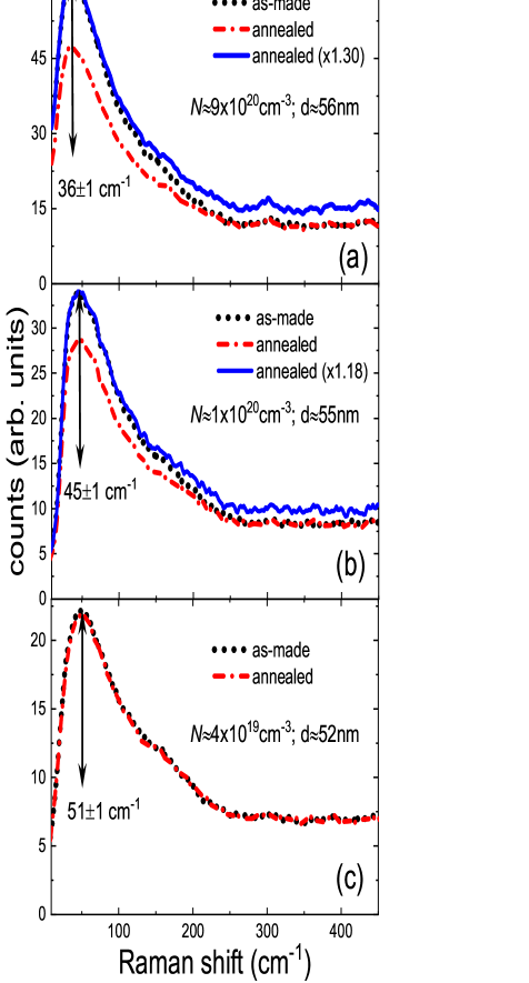
To cater for the spatial intensity-variations of the scattered signal the Raman spectra were normalized to the intensity of the as-made sample evaluated at 450cm (averaged value over the interval 440-450cm). This will be referred to as a ”background” intensity I. The ratio I/I, where Iis the intensity at the BP maximum, turns out to be a meaningful measure of the BP magnitude; I taken at different points across a given specimen may vary by more than 30% while I/I appears to be constant to better than 2% 25 .
Qualitatively, the Raman spectra for the three batches in Fig.2 exhibit the same BP shape characteristic of other amorphous and glassy systems 3 ; 4 ; 5 ; 6 ; 7 ; 8 ; 9 ; 10 ; 11 ; 12 ; 13 ; 14 ; 15 ; 16 . There are however two quantitative differences depending on the composition of the material. First, the peak position increases with the O-In ratio (Fig.3).
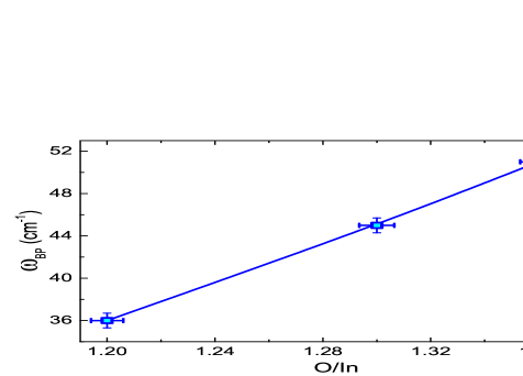
The position of the BP scales with the typical phonon energy of the material which is naturally smaller for the In-richer InO so this is just a consequence of the batch composition. That the peak-position appears at a frequency (O/In) and does not shift due to the thermal-treatment is consistent with the finding that the Hall coefficient is unchanged in the process 2 .
Secondly, the heat-treatment causes a more conspicuous decrease of the BP magnitude for the higher-N version while having indistinguishable change in the spectra of the low-N version despite the comparable change in the samples resistance during annealing. Also, for a comparable conductivity, the relative magnitude of the BP, is larger the higher is the carrier-concentration.
The amount of disorder required to affect a given change of the conductivity (or k) in a degenerate Fermi system like InO grows with the Fermi-energy (thus with N). This correlation was demonstrated in the dependence of the optical gap on k studied in-situ in 2 . Figure 4 shows three curves from this study for samples with carrier-concentration that are close to these of the batches studied in Fig.2. Note that, for a comparable change of k a larger change of the optical-gap occurred for the sample with the higher carrier-concentration, a similar trend to that observed in the dependence of the BP on disorder (Fig.2). The relative change of the BP magnitude presumably reflects the degree of the structural-change that occurred during heat-treatment. The correlation between disorder (either chemical or electronic) and I/I (table 1) has the same reason - for a comparable k higher disorder yields a more conspicuous BP demonstrating the common observation related to the phenomenon 12 .
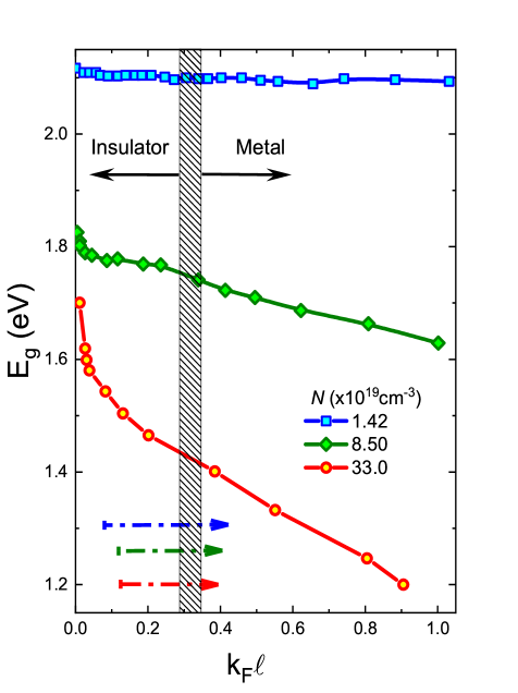
Table 1 includes the relative magnitude of the BP before and after annealing, with the batch chemical-disorder [O/In], and a quantitative measure of disorder W based on data of electronic-transport. The chemical disorder is taken here as the deviation of the composition from that of the stoichiometric InO compound. W is the critical disorder that Anderson-localizes the particular batch. WEN where E, is the Fermi energy. For InO the proportionality factor between disorder and Fermi-energy was found to be: W6.2·E 2 and E of a given batch is obtained using free-electron formulae.
| [O/In] | W (eV) | I/I as-made | I/I annealed |
|---|---|---|---|
| 0.3 | 2.21 | 5.3 | 4.2 |
| 0.2 | 0.51 | 4.1 | 3.4 |
| 0.14 | 0.28 | 3.1 | 3.1 |
Table 1: Values of parameters for the three InO batches measured in Fig.2. The electronic disorder (characterized by k) includes the contribution of the deviation from stoichiometry that may is relevant for phonon scattering vs. electron scattering discussed in the text below. Note the systematic dependence of the BP magnitude on the batch disorder.
III.2 Structural changes resulting from the heat-treatment
Before proceeding with further analysis of the Raman spectra we digress now to see what actually changes in the system micro-structure due to heat-treatment. This was done by using customary tools of structural analysis; X-ray and electron microscopy. Special emphasis was given to the high-N version of InO where the effect in terms of Raman spectroscopy is manifestly large. Consider first the electron-diffraction and TEM images for a typical sample shown in Fig.5a and Fig.5b:
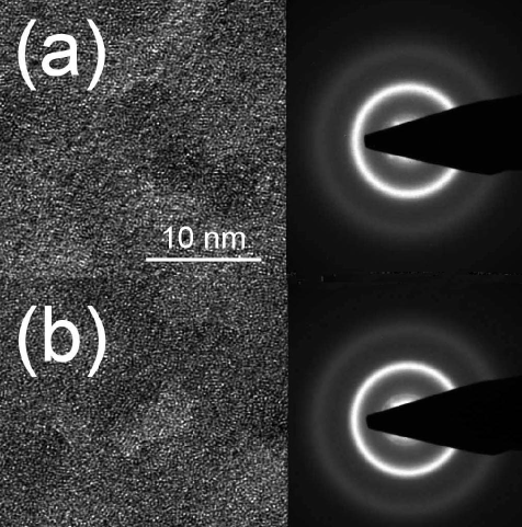
Both diffraction patterns exhibit broad rings characteristic of amorphous structure with no sign of crystallization. In fact, it is hard to see difference in the before and after patterns. On closer examination, the first strong ring in the pattern is sharper in the annealed sample and the associated bright-field image appears somewhat softer.
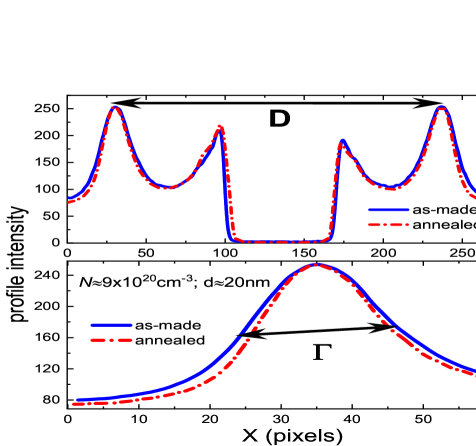
The changes in the diffraction pattern may be quantified by recording the intensity profiles of the diffraction patterns as is illustrated in Figure 6. The measurement confirms the eye-impression; the width of the ring decreased by 12% in the annealed sample. At the same time, the average ring-diameter indicated by D in the figure, increased by 0.40.1% suggesting a reduced interatomic separation due to annealing.
Similar results were obtained from XRD measurements on this high-N sample as shown in Fig.7.
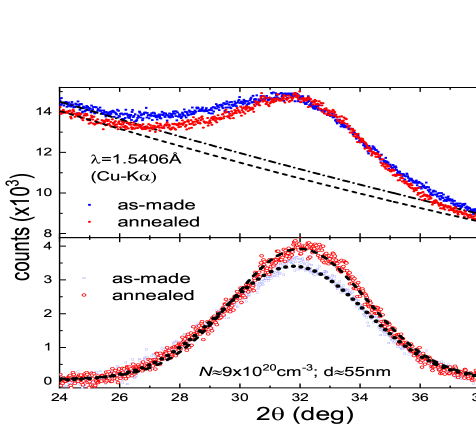
The small differences between the XRD and electron-diffraction in terms of the changes in D and ring-width may be due to the different substrates used.
On the basis of these measurements one might conclude that the volume-change -V/V of this sample due to the thermal-treatment is of the order of 1.2% to 1.8%. However, the results of XRR measurement suggest that V/V for this sample may be significantly larger (Fig.8a); Following treatment the sample thickness was reduced by 3.3% implying a volume-change -V/V of the order of 10%. Similar -V/V values during heat-treatment were obtained in a previous study of InO 2 . The difference in -V/V derived from the XRD versus that of the XRR suggest that the InO structure is made-up of loosely packed aggregates of relatively dense material. Such a porous medium is common in vapor-deposited films and more generally in substances that were quench-cooled from high temperatures. Actually, porosity is an abundant property of many materials. An extreme example of such a structure is a cotton-ball or a bundle of steel-wool. The volume of these substances may be greatly reduced when pressed while their solid part remains essentially intact.
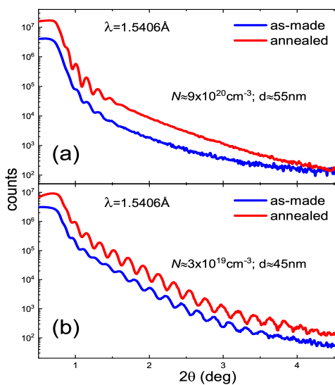
Figure 8b shows the XRR trace taken of a low-N sample that was added for comparison. It exhibits a quantitatively different behavior than the high-N sample in two aspects; the visibility of the interference extends over a wider range of angles, and the change of thickness during heat-treatment is much smaller (per the same change of the sample resistance). Note that heat-treatment enhanced the interference visibility in both samples yet the low-N sample retains a smoother film surface even when its resistance is considerably higher. Evidently, for a similar k, the high-N version of InO is both, more disordered and has a rougher surface.
To understand how structural aspects affect conductivity and the BP it may be useful to review the specific ingredients responsible for scattering in InO films.
III.3 The elements of disorder in amorphous indium-oxide films and their effect on conductivity and the boson-peak
As amorphous material InO lacks long-range order which by itself imposes limit on charge mobility. The vacuum deposited InO films have ancillary sources of disorder that lead to scattering and restrict their k value. First, there is an off-diagonal disorder in the material that is related to the distributed nature of the inter-atomic separation. The distribution of inter-particle distances gets narrower as the volume decreases and the system approaches the ‘ideal’ closed-packed amorphous structure. This enhances wavefunction overlap and therefore it naturally affects the conductivity. The diminishment of off-diagonal disorder during heat-treatment is clearly reflected in the reduced width of the electron-diffraction and in the XRD patterns (Figs.5,6 and Fig.7 respectively). The latter has been often associated with the appearance of medium-range order in the system 7 . This re-structure process is also reflected in the rate-distribution of the glass dynamics 23 . The ‘free-volume’ of the sample that is presumably eliminated is probably the most important single element in giving rise to phonon scattering. In fact, a porous nature of amorphous structures has been shown by detailed simulation studies to be the major contributing factor in the BP magnitude 12 .
A clear correlation between a structural-change and a modified BP is manifested in our study whenever a significant change of density takes place. This is observed most conspicuously for the heat-treated high-N sample where density is reduced by 10% (Fig.8a) and the Raman spectrum shows a 30% reduction in magnitude (Fig.2a). The correlation with the material density follows the trend reported in experiments on other disordered systems where the magnitude of the BP was observed to be smaller following densification by pressure 26 ; 27 ; 28 ; 29 ; 30 ; 31 ; 32 ; 33 ; 34 ; 35 .
The main difference between heat-treatment and applying high pressure appears to be the shift of the BP position to higher energy in the pressure experiments 26 ; 27 ; 28 ; 29 ; 30 ; 31 ; 32 ; 33 ; 34 ; 35 whereas no such shift is encountered in the Raman spectra for the thermally-annealed samples. In this regard the evolution of the BP shape in our experiments followed the heterogeneously-distributed elastic-constants scenario described by Schirmacher and Ruocco 8 . A similar behavior to our annealing experiments was observed in the BP spectra of AsS samples after it was cold-quenched from a well-annealed state 36 .
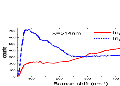
Another source of disorder in the amorphous indium-oxide system is associated with deviation from stoichiometry - chemical disorder. Relative to the ionic compound InO, there are 5-30% oxygen vacancies in InO spanning the range 10-5x10cm in terms of carrier-concentration. To preserve chemical neutrality some indium atoms must assume a valence of +1 instead of the +3 they have in the stoichiometric compound. When randomly distributed this valence-fluctuation forms a background potential with an amplitude of the order of few eV (assuming an average interatomic-separation of the order of 0.3nm). This type of disorder is quite prevalent in non-stoichiometric compounds, metallic-oxides, high-Tc materials etc. and it seems to be a main source of elastic scattering in both InO and InO 37 . On the other hand the role chemical-disorder plays in the buildup of a BP is unclear. Deviation from stoichiometry unaccompanied by other factors, does not necessarily promote formation of a BP; Polycrystalline films of InO exhibits 5-8% oxygen vacancies 37 while showing very small magnitude of BP relative to the amorphous version 38 . This probably means that oxygen vacancies and larger pockets of free-volume such as di-vacancies, are evenly distributed such that density-fluctuations over a phonon wavelength are rather small.
Finally, the reduction of surface roughness during the heat-treatment revealed in the XRR data needs elaboration. Changes in the interference visibility presumably reflect re-arrangement of ions at the film surface. This seems to occur even when changes in thickness were too small to be observed (see, Fig.8b). In principle, a rough film surface is a source of scattering for both phonons and electrons, and it is natural to expect less scattering when the surface roughness is reduced. Given that the mean-free-path in our samples is much smaller than the film thickness, the contribution of the surface to scattering by either electrons or phonons is probably very small. Electrical conductivity is sensitive enough to detect a small change of disorder in the sample. For phonons however the same structural change may be too small to affect the BP magnitude (Fig.2c). In other words, a measurable change in conductivity may be affected without a significant structural change, in similar vein with the dependence of the optical-gap E on k for a low-N sample where E remains almost constant while k changes over a large range (Fig.4).
IV Summary
We have followed by transport, structural-tools, and Raman spectroscopy the changes that occur during heat-treating InO films. Transport measurements were used to quantify the degree of disorder in InO samples with different carrier-concentrations before and after treatment. The disorder is characterized by assigning each sample a Ioffe-Regel parameter k. The study reveals a correlation between the system disorder defined in this way, and the magnitude of the BP. This correlation suggests that, in these systems, phonons are scattered by the same elements of disorder that cause scattering of electrons although not necessarily with the same efficiency.
An element of disorder that has a large effect on the BP magnitude is the presence of ‘free-volume’ in the system that, in InO is presumably related to the spatial distribution of oxygen vacancies. These are re-arranged during the annealing process to reduce the system volume, and the BP magnitude is changed accordingly. Our study furnishes the experimental support to the simulation work of Shintani and Tanaka that identified the most conspicuous BP in low-density defective structures 12 . This led them to conclude: ”…the origin of the boson peak (are) transverse vibrational modes associated with low-density defective structures” 12 .
The emerging picture is that heat-treating InO is analogous to the process of gently tapping a ground-coffee bag to pack it tighter. Tapping supplies the energy necessary to overcome local barriers allowing the powder to reduce its gravitational energy. Temperature and the interparticle-attraction respectively play the analogous roles in the process of densifying InO. Enhanced conductivity due to densification follows from enhanced wavefunction overlap as well as from improved connectivity. This is accompanied by a reduced disorder and therefore weaker heterogeneity which is reflected in a smaller magnitude of the BP. The flexibility that the InO system offers in terms of fine-tuning disorder by heat-treatment makes it a prime candidate for the study of electronic transport in glasses, and as demonstrated in this work, also for other fundamental properties of amorphous materials.
Acknowledgements.
We benefitted from discussions with Walter Schirmacher and Alessio Zaccone. The assistance of Anna Radko, Vladimir Uvarov, and Inna Popov from the Center for Nanoscience and Technology (HU) is gratefully acknowledged. This research has been supported by the 1030/16 grant administered by the Israel Academy for Sciences and Humanities.References
- (1) H. Wiesmann, M. Gurvitch, A. K. Ghosh, H. Lutz, O. F. Kammerer, and Myron Strongin, Estimate of density-of-states changes with disorder in A-15 superconductors, Phys. Rev. B 17, 122 (1978); M, Gurvitch, A. K. Ghosh, H. Lutz, and M. Strongin, Low-temperature resistivity of ordered and disordered A15 compounds, Phys. Rev. B 22, 128 (1980); M. Putti, R. Vaglio and J.Rowell, Radiation damaged MgB2: a comparison with A15 superconductors, Journal of Physics: Conference Series 97 012327 (2008),
- (2) Z. Ovadyahu, Memory versus irreversibility in the thermal densification of amorphous glasses, Phys. Rev. B 95, 214207 (2017).
- (3) V.K. Malinovsky and A.P. Sokolov, The nature of the boson peak in Raman scattering in glasses, Solid State Com., 57, 757 (1986).
- (4) S. R. Elliott, A Unified Model for the Low-Energy Vibrational Behavior of Amorphous Solids, EPL 19 201 (1992)
- (5) Walter Schirmacher, Gregor Diezemann, and Carl Ganter, Harmonic vibrational excitations in disordered solids and the “boson peak”, Phys. Rev. Lett. 81, 136 (1998).
- (6) N. N. Ovsyuk and V. N. Novikov, Influence of structural disorder on Raman scattering in amorphous porous silicon, Phys. Rev. B 57, 14615 (1998).
- (7) S. Sugai and A. Onodera, Medium-Range Order in Permanently Densified SiO and GeO Glass, Phys. Rev. Lett. 77, 4210 (1996).
- (8) Walter Schirmacher and Giancarlo Ruocco, Heterogeneous Elasticity: The tale of the boson peak, arXiv:2009.05970v1 [cond-mat.dis-nn]
- (9) S. N. Taraskin and S. R. Elliott, Phonons in vitreous silica: Dispersion and localization, Europhys. Lett., 39 (1), 37 (1997).
- (10) J. S. Lannin N. Maley and S. T. Kshirsagar, Raman scattering and short range order in amorphous germanium, Solid State Com., 53, 939 (1985).
- (11) M. Baggioli and A. Zaccone, Unified theory of vibrational spectra in hard amorphous materials, Phys. Rev. Research 2, 013267 (2020).
- (12) H. Shintani and H. Tanaka, Universal link between the boson peak and transverse phonons in glass, Nature Mater. 7, 870 (2008).
- (13) Vassiliy Lubchenko and Peter G. Wolynes, The origin of the boson peak and thermal conductivity plateau in low-temperature glasses, PNAS, 100, 1515 (2003).
- (14) V. L. Gurevich, D. A. Parshin, and H. R. Schober, Pressure dependence of the boson peak in glasses, Phys. Rev. B 71, 014209 (2005).
- (15) K. Niss, B. Begen, B. Frick, J. Ollivier, A. Beraud, A. Sokolov, V. N. Novikov, and C. Alba-Simionesco, Influence of pressure on the boson peak: stronger than elastic medium transformation, Phys. Rev. Lett. 99, 055502 (2007).
- (16) H. R. Schober, U. Buchenau, and V. L. Gurevich, Pressure dependence of the boson peak in glasses: Correlated and uncorrelated perturbations, Phys. Rev. B 89, 014204 (2014).
- (17) N. F. Mott and A. E. Davis, electronic Processes in Non-Crystalline Materials, Oxford University (1971).
- (18) K. A. Blanks, The role of the Raman coupling coefficient in an inelastic light scattering process in amorphous solids, Journal of Non-Crystalline Solids, 208, 81 (1996); A. Fontana, R. Dell’Anna, M. Montagna, F. Rossi, G. Viliani, G. Ruocco, M. Sampoli, U. Buchenau and A. Wischnewski, The Raman coupling function in amorphous silica and the nature of the long-wavelength excitations in disordered systems, Europhys. Lett., 47, 56 (1999); Bernhard Schmid and Walter Schirmacher, Raman Scattering and the Low-Frequency Vibrational Spectrum of Glasses, Phys. Rev. Lett. 100, 137402 (2008).
- (19) D. Shahar and Z. Ovadyahu, Superconductivity near the Mobility Edge, Phys. Rev. B 46, 10917 (1992).
- (20) U. Givan and Z. Ovadyahu, Compositional disorder and transport peculiarities in the amorphous indium-oxides, Phys. Rev. B 86, 165101 (2012).
- (21) See Supplemental Material at [URL will be inserted by publisher] for fuller details of the two setups used for Raman spectroscopy and associated data.
- (22) Z. Ovadyahu, Slow dynamics of the electron-glasses; the role of disorder, Phys. Rev. B. 95, 134203 (2017).
- (23) Z. Ovadyahu, Structure dynamics in thermal-treatment of amorphous indium-oxide films, Phys. Status Solidi B 257,1900310 (2020).
- (24) Yu. M. Galperin, V. L. Gurevich and D. A. Parshin, Theory of low-temperature thermal expansion of glasses, Phys. Rev.B 32, 6873 (1985).
- (25) See figure S4 in Supplemental Material at [URL will be inserted by publisher] for an example.
- (26) L. Orsingher, A. Fontana, E. Gilioli, G. Carini, G. Carini, G. Tripodo, T. Unruh, and U. Buchenau, Vibrational dynamics of permanently densified GeO glasses: Densification-induced changes in the boson peak, J. Chem. Phys. 132, 124508 (2010).
- (27) T. Deschamps, C. Martinet, D. de Ligny, J. L. Bruneel, and B. Champagnon, Correlation between boson peak and anomalous elastic behavior in GeO2 glass: An in situ Raman scattering study under high pressure, J. Chem. Phys. 134, 234503 (2011).
- (28) J. Schroeder, W. Wu, J. L. Apkarian, M. Lee, L.-G. Hwa, C. T. Moynihan, Raman scattering and Boson peaks in glasses: temperature and pressure effects, J. Non. Cryst. Solids 349, 88 (2004).
- (29) M. Ahart, D. Aihaiti, R. J. Hemley, and Seiji Kojima, Pressure dependence of the Boson peak of glassy glycerol, J. Phys. Chem. B 121, 6667 (2017).
- (30) B. Mantisi, S. Adichtchev, S. Sirotkin, L. Rafaelly, L. Wondraczek, H. Behrens, C. Marcenat, N. V. Surovtsev, A. Pillonnet, E. Duval, B. Champagnon, and A Mermet, Non-Debye normalization of the glass vibrational density of states in mildly densified silicate glasses, J. Phys.: Condens. Matter 22, 025402 (2010).
- (31) V. L. Gurevich, D. A. Parshin, and H. R. Schober, Pressure dependence of the boson peak in glasses, Phys. Rev. B 71, 014209 (2005).
- (32) L. Hong, B. Begen, A. Kisliuk, C. Alba-Simionesco, V. N. Novikov, and A. P. Sokolov, Pressure and density dependence of the boson peak in polymers, Phys. Rev. B, 78, 134201 (2008).
- (33) M. Zanatta, G. Baldi, S. Caponi, A. Fontana, E. Gilioli, M. Krish, C. Masciovecchio, G. Monaco, L. Orsingher, F. Rossi, G. Ruocco, and R. Verbeni, Elastic properties of permanently densified silica: A Raman, Brillouin light, and X-ray scattering study, Phys. Rev. B 81, 212201 (2010).
- (34) A. Monaco, A. I. Chumakov, G. Monaco, W. A. Crichton, A. Meyer, L. Comez, D. Fioretto, J. Korecki, and R. Rüffer, Effect of densification on the density of vibrational states of glasses, Phys. Rev. Lett. 97, 135501 (2006).
- (35) E. Stavrou, C. Raptis, and K. Syassen, Effects of pressure on the boson peak of tellurite (TeO)(ZnO) glasses: Evidence of an elastic glass-to-glass transition, Phys. Rev. B 81, 174202 (2010).
- (36) V.K. Malinovsky and A.P. Sokolov, The nature of the boson peak in Raman scattering in glasses, Solid State Com., 57, 757 (1986).
- (37) Z. Ovadyahu, B. Ovryn and H.W. Kraner, Microstructure and electro-optical properties of evaporated indium-oxide Films, J. Elect. Chem. Soc. 130, 917 (1983).
- (38) See figure S3 in [21].
V Supplementary Material
This part and the following subsections give auxiliary information related to the methods and techniques employed in the study.
V.1 Avoiding crystallization
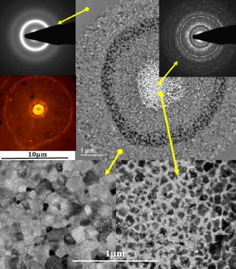
One should realize that the crystalline version of indium-oxide, InO differs markedly from these amorphous versions that are investigated here. InO may be easily crystallized to form polycrystalline InO once exposed and maintained at temperatures as low as 380K (depending on the InO composition).The danger of InO crystallization must be taken into account especially when exposing the film to intense laser radiation but also during heat-treatment. Keeping the heat-treatment temperature below 370K practically eliminates crystallization problems; we never encountered a problem with heat-treatment even when the sample was left for 34 days at this temperature. It is more complicated to set a limit for the laser power because it depends on the heat-dissipation through the substrate. To assist in identifying the threshold we carried an experiment designed to observe the onset of structural changes using high-resolution TEM. The results are shown in Fig.9 and Fig.10:
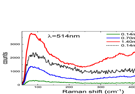
On the basis of the correlation between these structural and Raman data we identify the spectra taken with 0.7mW and 1.4mW laser power as a signature of partial crystallization, or a highly defected polycrystalline phase (see Fig.11 for typical spectrum of well-annealed InO that lacks the pronounced BP observe in the laser-exposed plots in Fig.9). This signature was used in the study to set the power-limit on samples deposited on Si-wafers. The latter exhibit more efficient heat-dissipation than the carbon film used for the TEM work allowing a larger laser power to be used (see text).
V.2 Low-energy Raman setup
A home-built ultra-low frequency Raman confocal system was assembled and optimized for measurements of Raman spectra down to 10cm. The setup included an exciting-source Nd:YAG laser (CNI, MSL-FN-532), and the scattered signal was collected via high throughput 532 longpass nano-edge filters (NEFs) and a single spectrometer.
In particular, a single longitudal mode doubled Nd:YAG laser (CNI, MSL-FN-532) beam from a diode-pumped solid-state laser was directed toward a reflecting Optigrate band-pass filter, based on the volume Bragg-grating technique for cleaning up the laser spectral noise and resulting in spectral widths 7 cm. Then two mirrors were used to aim the reflected laser beam towards a 532 NEF (Iridian spectral technologies) with deep blocking (OD 6) at the laser line, set in an adjustable filter holder. The combination of the mirrors with the NEF1, allowed to adjust the angle between the incident laser beam and the normal of NEF1 for gaining the best laser line attenuation and the lowest possible frequency of the ULF Raman signal, as well as to reflect the beam to the microscope objective. The laser beam was focused through a X50/0.65 microscope objective to provide a 3 mW incident beam on the sample, which also collected and collimated the back scattered Rayleigh and Raman signals. The backscattered signal passed through the above mentioned NEF1, partially filtering the signal and then through an additional filter, NEF2, to achieve the desirable attenuation of the Rayleigh signal. Following the passage through the filters, the signal was focused by a 10 cm focal length plano-convex lens onto a pinhole (100 m), located in front of a 10 m slit of a 0.14 m Czerny-Turner spectrometer (Jobin-Yvon, MicroHR) with an entrance aperture ratio of f/3.88, with a 1200 g/mm grating. Finally, the signal was detected by an air cooled 1,024 x 1,024 intensified charge-coupled device (Andor, DH734-18U), driven by the Solis 4.3 software and analyzed. The system can achieve spectral resolution at the full-width half-maximum of a peak in the spectrum of up to 11 cm. The spectra of the samples mentioned below were measured under similar conditions with the detector operated at integration times of 15 min.
V.3 Spectra normalization
To get a good signal to noise and avoid risk of crystallization calls for compromises. The laser spot used had a diameter of 2m (Renishaw setup) and 2.7m (BGU setup) and the question of sample uniformity being typically 1x1cm, had to be tested. Taking advantage of the computerized Invidia (Renishaw) features, several runs of 25 spots on a sample were taken for statistics purposes. These 25 scans were taken consecutively on a 0.1x0.1mm square (5 rows, 5 columns). The Raman signal in the interval 440-450cm was averaged for each of the 25 traces and the histogram of these values is shown in Fig.12:
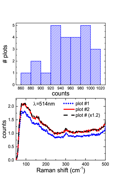
The figure also includes the spectra for two traces for which the variation in the magnitude of the signal is the greatest and it is illustrated that they can be made to overlap by multiplying by a constant factor. On basis of such measurements we opted for normalizing the curves using I as the reference (see Fig.2 of the main text).