Externally controlled and switchable 2D electron gas at the Rashba interface between ferroelectrics and heavy metals
Abstract
Strong spin-orbit coupling in noncentrosymmetric materials and interfaces results in remarkable physical phenomena, such as nontrivial spin textures, which may exhibit Rashba, Dresselhaus, and other intricated configurations. This provides a promising basis for nonvolatile spintronic devices and further implications. Here, we simulate from first principles a two-dimensional electron gas in ultrathin platinum and palladium layers grown on ferroelectric PbTiO3(001). The latter allows, in principle, to switch and control the spin-to-charge conversion by the polarization reversal. We show how the band structure and its Rashba splitting differ in the Pt and Pd overlayers and how these electronic features change with increasing the overlayer thickness and upon reversal of polarization. Besides, for both overlayers, we simulated their current-voltage () characteristics, the resistance of which upon the polarization reversal changes between 20 % and several hundred percent. The reported findings can be used to model directly the Rashba-Edelstein effect.
I Introduction
Reversal of polarization in ferroelectrics (FE) which is achieved by applying an electric field allows to induce nonvolatile electrons or, alternatively, holes into the material which overlays the FE substrates. [1] So far, however, in the context of a two-dimensional electron gas (2DEG), research focuses mostly on the TiO2-terminated (001) surface of paraelectric SrTiO3 (STO). The 2DEG emerges there beneath epitaxially grown LaAlO3 (LAO) [2] or similar polar perovskites [3, 4]. Presently, the nature of this 2DEG and the role of polar overlayers are well understood (see Refs. 5, 6 and references therein). LAO/STO(001), for instance, shows its 2DEG mobility which is one order of magnitude higher than that of silicon based transistors. Moreover, the STO interface with some defective oxides possesses 2D superconductivity [7, 8, 9] and induced magnetism seen as anomalous Hall effect in magneto-transport measurements. [10]
Alternatively, the 2DEG emerges in STO(001) by the deposition of ultrathin film of Al or some other reactive metals. [11, 12, 13] The metal overlayer partially pulls out oxygen from STO and transforms into binary oxide. Meanwhile, the upper 1-nm-thick layers of STO become oxygen-deficient and marginally polar. In this scenario, the broken inversion symmetry at the 2DEG interface lifts spectral degeneracy that is known as the effect of Rashba spin-orbit coupling (SOC). [14] For instance, the Al/STO(001) shows at 2 K the electric-field-induced switchable polarization of 4C cm-2, while the 2DEG exhibits a sizable Rashba SOC [15] with relatively high conversion efficiency. [16]
A spin-orbitronic concept of the FE-controlled spin–to.charge conversion has been suggested recently by P. Noël et al. [17] who demonstrate this phenomenon experimentally using NiFe(20 nm)/Al(0.9 nm)/STO. [17]
The authors show how the nonmagnetic Rashba system efficiently generates spin current from charge current due to the Rashba-Edelstein effect [18]. The breaking of inversion symmetry at the interface results in the out-of-plane electric field. Then, the in-plane charge current via interfacial 2DEG produces a transverse spin density, which can diffuse as a spin current into the adjacent material [19]. Conversely, the injection of a spin current into the Rashba state will produce the charge current due to the inverse Edelstein effect [20]. Most importantly, the FE polarization reversal changes the sign of the local electric field that reverses the chirality of the spin textures in the both Rashba-split Fermi contours (see Fig. 1 of Ref. 17). On the other hand, the charge current sign, generated through the inverse Edelstein effect, should depend on the FE polarization state. This mechanism offers the basis for the bipolar memory device and other logic devices. [21]
This work was motivated by the interconverting charge and spin currents through the direct and inverse Edelstein and spin Hall effects. [22, 23, 16, 17, 24, 25, 26, 27] When the robust ferroelectric substrate, such as PbTiO3(001) (PTO), is used instead of the STO 2DEG, this makes possible to extend the ordinary electric-field dependence of Rashba SOC [15, 28] to its switching option since the polarization reversal may accumulate/deplete 2DEG electrons. Highly reactive metal is not needed now for the overlayer material. Here, we simulated from first principles the 2DEG in the few-monolayer-thick nonmagnetic metals (): Pd and Pt. In this scenario, the formation of 2DEG moves from the two upper layers of STO into the metal overlayer. Therefore, the picture of Rashba SOC changes. In the O deficient ABO3 perovskite layer, the Fermi level crosses the bottom B-cation conduction band, which is splitted by SOC into two parabolas around the point of the Brillouin zone. In the case of /PTO ( Pd, Pt), its 2DEG is formed by multiple -branches that is typical for the heavy d-metal and broken inversion symmetry.
It should be noted that the interfaces between perovskites and metals provoke the formation of oxygen vacancies, oxide layers and the intermixing of cations across the interface. The one-unit-cell steps can be also seen there. [29] It is established now that perovskites grow in complete unit cells while their (001) surfaces are usually TiO2-terminated. To obtain the PbO-terminated PTO, a special procedure is required. [30] The interfacial defects in multiferroic tunnel junctions reduce the functional insulating thickness of the barriers [31] whereas the functionality and weakly degrading properties of electrodes are not characterized. The issue of PTO(001) passivated by Pb was discussed in Ref. 32. Using the angle-resolved x-ray photoemission spectroscopy, the authors found that metallic Pb diffuses into the Pt layer during the Pt deposition on PTO(001) thin films. As the result, a defective layer at the Pt/PTO(001) interface produces the observed Fermi energy pinning. Obviously, the Pt overlayers diluted by Pb retain many properties of ideal material, including the screening of the FE dipole. Since Pb is a heavy chemical element, the Pb substitute should not affect the Rashba SOC significantly. We relaxed the chemically perfect and TiO2-terminated interfaces of metal/PTO only. In principle, to obtain the spin-to-charge conversion the nonmagnetic-metal/PTO system needs to be covered by an extra layer of NiFe. Here, we do not model the effect of proximity to the ferromagnetic layers.
Focusing on the Rashba SOC in 2DEG of dually polar Pd/PTO and Pt/PTO, we calculated and compared their band structures. Besides, the distinguished Rashba splittings are evaluated. Finally, electroresistance and its dependence on the polarization reversal as well as the overlayer thickness are presented that was not performed so far. We anticipate that the relative resistance, calculated as (P) - (P)(P, changes, depending on the number of metallic overlayers, between 20 % and more than 400 %. Thus, the findings reported may attract extensive attention.
II Details of calculations
In all ab initio calculations performed here, the TiO2-terminated PTO(001) was modeled using a reliable set-up, within the slab geometry with a vacuum layer. [33] Over the past decade, the interfaces between the TiO2-terminated perovskites and metals were studied in the context of multiferroic tunnel junctions, in which the FE barrier is placed between two ferromagnetic electrodes that enables four distinct resistance states. [34, 35] That is why the ferromagnetic 3 metals, mainly, and some other ferromagnetic compounds adjusted as electrodes were simulated. [36, 29, 37, 31, 38, 39, 40, 41, 42, 43, 44, 45, 46] Curiously, despite relatively strong magneto-electric coupling detected for all these FE/ferromagnetic interfaces, the robustly switched magnetic order of electrodes due to the barrier polarization reversal was not evidenced until now.
Regarding the nonmagnetic electrode materials, the 4 and 5 f.c.c. metals represent the most suitable option. In particular, the lattice mismatch between PTO and Pd (Pt) is less than 0.7 % (1.5 %). The Pt/BaTiO3 interface is well studied experimentally and theoretically from first principles. [47, 48, 49] As for Pd/PTO and Pt/PTO, so far only the latter interface was simulated from first principles. [50] However, the structure changes and, especially, the changes in the 2DEG, occurring upon the PTO polarization reversal at the presence of Rashba SOC, need a more detailed consideration.
To treat the interplay between electronic and structural properties of ferroelectric PTO(001) and ultrathin Pt(Pd) overlayers, we used the two density functional theory (DFT) packages: the Vienna Ab initio Simulation Package (VASP) [51] and QuantumATK package [52]. The idea of using these different codes for the same material is not to evaluate their accuracy, although we keep in mind this double-check. The VASP has the plane-wave basis set, which provides more accurate energetics and structural optimization, while QuantumATK allows to simulate the semi-infinite supercell. It is important to demonstrate that the set up of finite and relatively thin supercell can mimic well the ferroelectric PTO(001). Here, we performed the test calculation using this semi-infinite option of QuantumATK. The second reason of using QuantumATK is its transport implementations which allow to simulate the electroresistance in /PTO.
The geometric relaxations were obtained by VASP. The thickness of metallic overlayers varies between one and three monolayers (ML) with two Pt(Pd) per ML. All these metallic atoms as well as atoms of the 2-u.c.-thick PTO near the interface were allowed to relax. Beneath that, to mimic semi-infinite FE, we kept the 3-u.c.-thick PTO fixed, optimized already for each of its two directions of polarization. The electron-ion interactions within VASP calculations were described by the projector-augmented wave pseudopotentials and the electronic wave functions were represented by plane waves with an energy cutoff of 450 eV. Although we focus here on the Perdew-Burke-Ernzerhof (PBE) generalized-gradient approximation (GGA) [53] to the exchange-correlation potential, the local density approximation (LDA) within DFT, was used as well. The P and P configurations of /PTO were relaxed separately for each overlayer material and for each thickness 1,2,3. Ionic relaxation in the Me overlayers and layers of PTO beneath the interface was performed using the conjugate-gradient algorithm until the Hellmann-Feynman forces became less than eV/Å. The use of the k-mesh yielded the reliable atomic positions. The density of states (DOS) was obtained then using the tetrahedron method on the -centered and compacted k-mesh with no smearing for the electronic occupations. A cross-check of the interface structure and Rashba SOC on the electronic states was done using the QuantumATK package. Thus, various computed quantities were carefully compared among the two DFT codes to obtain consistent results while their reliability was achieved by numerous convergence tests.
To receive the layer-resolution of the DOS and band structure, we used the QuantumATK package which uses linear combinations of atomic orbitals (LCAO) as basis set. For all of these calculations we used the slab configuration optimized with VASP and applied a -centered k-point mesh and a density-mesh cutoff energy of 280 Ry and a broadening of 25 meV together with fully-relativistic norm-conserving PseudoDojo pseudopotentials. [54] Within this setup we calculated the fat bands and projected the DOS on each layer.
III Results and discussion
III.1 Structural properties and induced extra carriers
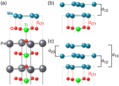
Here we focus on relaxed structure of the metal ( Pt, Pd) MLs. The outermost and key TiO2 layer of PTO(001) is denoted S, while the intralayer -displacements in each PTO layer, , are positive (negative) for P (P). The layers, which form tetragonally distorted f.c.c lattice, are indicated as S+1, S+2 and S+3. In the first layer, S+1, its two sites were relaxed either on top of the O sites (O/O) or on top of the PTO cation sites (Ti/Pb).
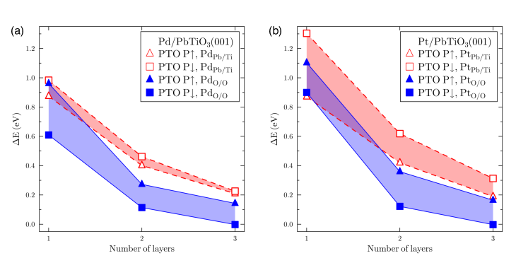
In Figs. 1 (a) and 1 (b), the energetics of relaxed (Pd2)/PTO (P) and (Pt2)/PTO (P) is shown, respectively, as a function of the thickness 1, 2, 3. For each case of the FE polarization P we subtracted the energy of relaxed substrate from the total energy of the system and then normalized the results per one atom. The lowest normalized energy, which corresponds to the (O/O) configuration of 3 and P P, was selected as the zero energy. Thus, Fig. 1 represents along its -axis the relative differences in energy, as compared to that of the lowest normalized difference. We found that the interfacial (O/O) configuration, with both atoms on top of oxygens of the P-poled PTO(001), is strongly energetically preferable, except one competitive case of 1-ML-thick Pt on PTO(P), where both Pt can sit above cations in configuration (Ti/Pb). The latter case is clearly seen in Fig. 1 (b). However, by placing the S+2 and S+3 layers, the (O/O) configuration becomes again notably preferable. Surprisingly, for the (Ti/Pb) interfacial configurations of the two overlayers whatever their thickness is, the polarization state P is favourable that contradicts to the configuration (O/O). For the latter, the P state of PTO is always favourable. Therefore, in the following we show and discuss the results obtained for the dually poled (O/O) configurations only. In general, by analyzing the results shown in Fig. 1, we find that the both systems Pd/PTO and Pt/PTO become energetically more stable for the thicker metallic overlayer, which obeys gradually the f.c.c. lattice starting from 3.
The structures after relaxation are given in Fig. 2.
We introduced there the interlayer structure parameters and collected all computed data in Tab. 1 for the two states of poled PTO and each . For 1, the interfacial Pd–O (Pt–O) distance, dO1 of 2.01 Å (2.00 Å), which is obtained for P, increases significantly upon polarization reversal to the value of 2.32 Å (2.61 Å). With increasing 1, the P-poled dO1 increases slightly by 0.03–0.05 Å for both metals, whereas the reversal to P diminishes dO1 by about 0.1 Å and 0.3 Å for Pd and Pt, respectively.
For 2 and Pd (Pt), the interlayer distance between S+1 and S+2, d12, increases from 1.92 Å (1.97 Å) by 0.02 Å (0.04 Å) when changes from P to P. Growing the third layer results in the 0.04 Å increase of d12 that is seen for both metals and each . Meanwhile, the separation S+2 and S+3, d23, shows the systematic and notable decrease of 0.07 Å, as compared to d12. For 3, the interlayer separation d13 between S+1 and S+3 gives an idea of the lattice parameter. Since the in-plane lattice parameter of 3.88 Å is fixed by the PTO substrate, we find that the first Pd unit cell is cubic while Pt is tetragonally elongated.
| dO1 | dO1 | dO1 | d12 | d12 | d23 | d13 | ||
|---|---|---|---|---|---|---|---|---|
| (1ML) | (2ML) | (3ML) | (2ML) | (3ML) | (3ML) | (3ML) | ||
| Pd | P | 2.01 | 2.04 | 2.03 | 1.92 | 1.96 | 1.89 | 3.86 |
| Pd | P | 2.32 | 2.23 | 2.20 | 1.94 | 1.98 | 1.91 | 3.88 |
| Pt | P | 2.00 | 2.04 | 2.05 | 1.97 | 2.03 | 1.96 | 3.98 |
| Pt | P | 2.61 | 2.32 | 2.33 | 2.01 | 2.02 | 1.95 | 3.97 |
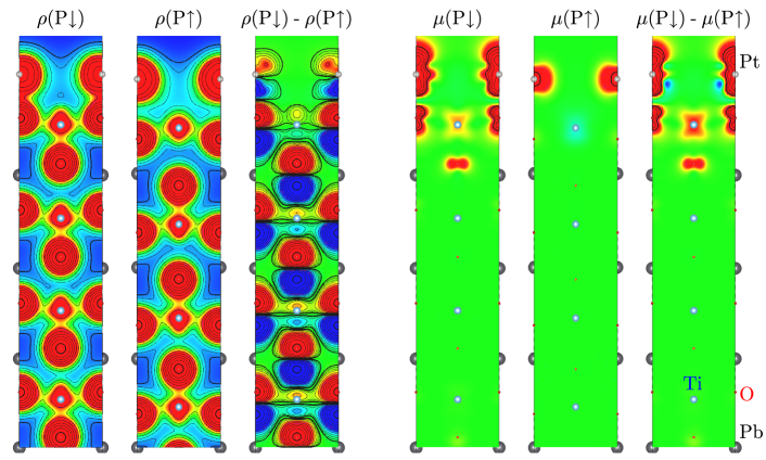
The changes in structure of /PTO, which occur due to the -reversal, redistribute charges in the system. This is illustrated for the case 1 and Pt in Fig. 3 where the charge density cut, , is plotted for each direction of as well as the charge differences (P)–(P). To compare the two densities and to plot the charge (magnetization) density difference in the third panel of Fig. 3, the positions of Pb in the layer (S-1) were coincided for P and P. The charges change dramatically in the PTO layers that is not surprising. However, the interface (S) and Pt layer (S+1) display also the charge redistribution. To evaluate this effect, we show in the lower panel of Fig. 4 the charge difference, calculated between the PTO polarizations P and P and plotted as a function of L. For Pd and for all L, the state P induces 0.04 electron per each Pd, as compared to P. The case of Pt is much more specific. For 1ML Pt, the P state of PTO creates 0.08 electron more than P. Then, with increasing L, the disbalance between P and P becomes marginal for 2 and, finally, for 3 P overcomes with 0.05 electron, i.e. the value similar to that of 3ML Pd.
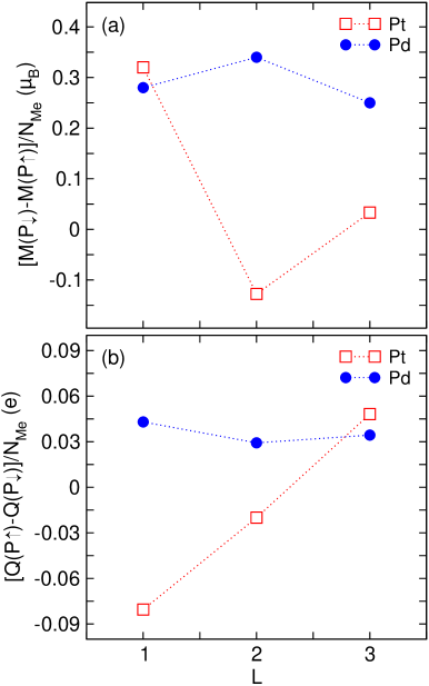
The thin film geometry of overlayer and extra electrons induced by PTO result in the magnetization densities, which are seen in Fig. 3 for dually polar 1ML Pt together with their difference cut (P)–(P). The magnetic moments were calculated using VASP for each . For Pd, the P polarization results in relatively small , which vary from 0.03 in the topmost layer of each to 0.18 . The -reversal induces the larger Pd moments which exceed 0.4 when 1. Since extra electrons fill in the minority spin band of the d-states, the corresponding charge increase reduces the value of induced magnetic moment. The case of Pt shows rather similar trend of induced magnetism, except Pt bilayer at P when all become marginal. This is because of relatively short interlayer separation that was discussed for iron bilayer on PTO. [39]
It should be noted that the targeting spin-to-charge conversion needs the next and robust ferromagnetic layer which covers nonmagnetic Me. That coverage may seriously reduce or even suppress the moments. Nevertheless, the scenario of switchable induced magnetization can be simulated here, in absence of ferromagnetic overlayer. In the top panel of Fig. 4, we plot the moment difference between P and P as a function of . As one can see there, Pd represents a reliable switch, indeed, whereas Pt seems less attractive because of the case of weakly magnetic 2.
III.2 2DEG and its band structure
| Position | |
|---|---|
| (1/Å) | |
| P | 0.031 |
| P | 0.070 |
| P | 0.052 |
| P | 0.053 |
| P | 0.079 |
| P | 0.057 |
It is well known that the density functional theory (DFT), within both, the GGA and LDA, underestimates the insulating band gap of ferroelectric PTO, whereas DFT+ [55, 56, 57] improves the gap value, when the appropriate correlation parameter is applied to the 3 orbitals of Ti. For instance, the use of enormous of 7 eV increases the gap of PTO to 2.7 eV which is, however, notably lower than the corresponding experimental value. Besides, the spin-polarized simulations of the multiferroic interfaces and tunnel junctions containing the PTO and PZT barriers [31, 41, 42, 44] showed before that DFT+ induces the artificial magnetic moments up to on each Ti. The slab geometry and proximity to the ferromagnetic material are responsible for that. Thus, we used here the DFT only. The calculated band gap of 1.5 eV keeps the insulating state for PTO and serves as a reliable starting point to simulate the 2DEG in /PTO. Concerning the questionable degree of electronic correlations in the Pd and Pt overlayers, their electronic states can be well described by DFT.
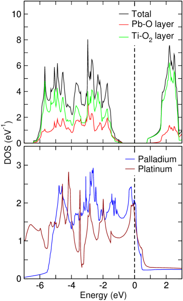
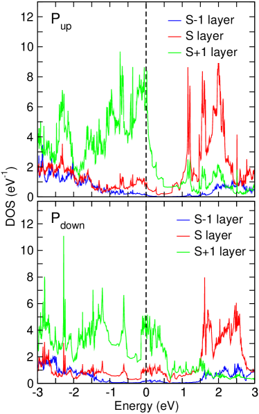
For bulk PTO, its total density of states (DOS) together with the layer-resolved (Pb-O and Ti-O2) contributions are shown in the upper panel of Fig. 5. The lower panel of Fig. 5 shows the DOS of Pd and Pt that gives an idea on how the PTO gap may be filled by the -overlayer bands. To analyze in details the 2DEG and related bands, which cross the Fermi level of /PTO(001) ( Pd, Pt), we plot in Fig. 6 the layer-resolved DOS of 1ML Pt/PTO. The DOS contributions from each atom of the layers S1, S and S+1 are plotted there. For the PTO polarization P, as the upper panel of Fig. 6 shows, the Pt states of the 2-Pt-atom layer S+1 dominate at while the PTO interfacial layer S contributes less significantly. The layer S1 (Pb-O) contributes marginally at indicating, therefore, the position of the former PTO band gap which extends above up to 1 eV. The lower panel of Fig. 6 shows that the polarization reversal to P notably decreases the DOS value . This is mostly due to reduction of the Pt -states whereas the S layer contribution changes insignificantly. Thus, we obtain a clear evidence that the PTO polarization reversal should dramatically change the 2DEG carrier density in /PTO(001).
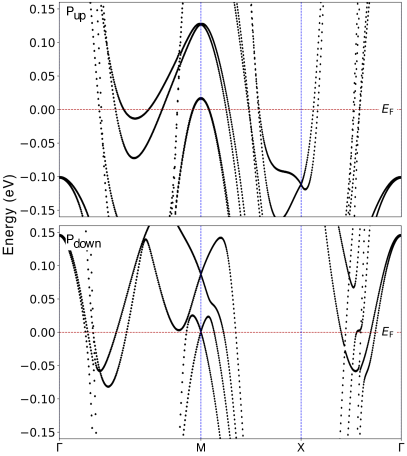
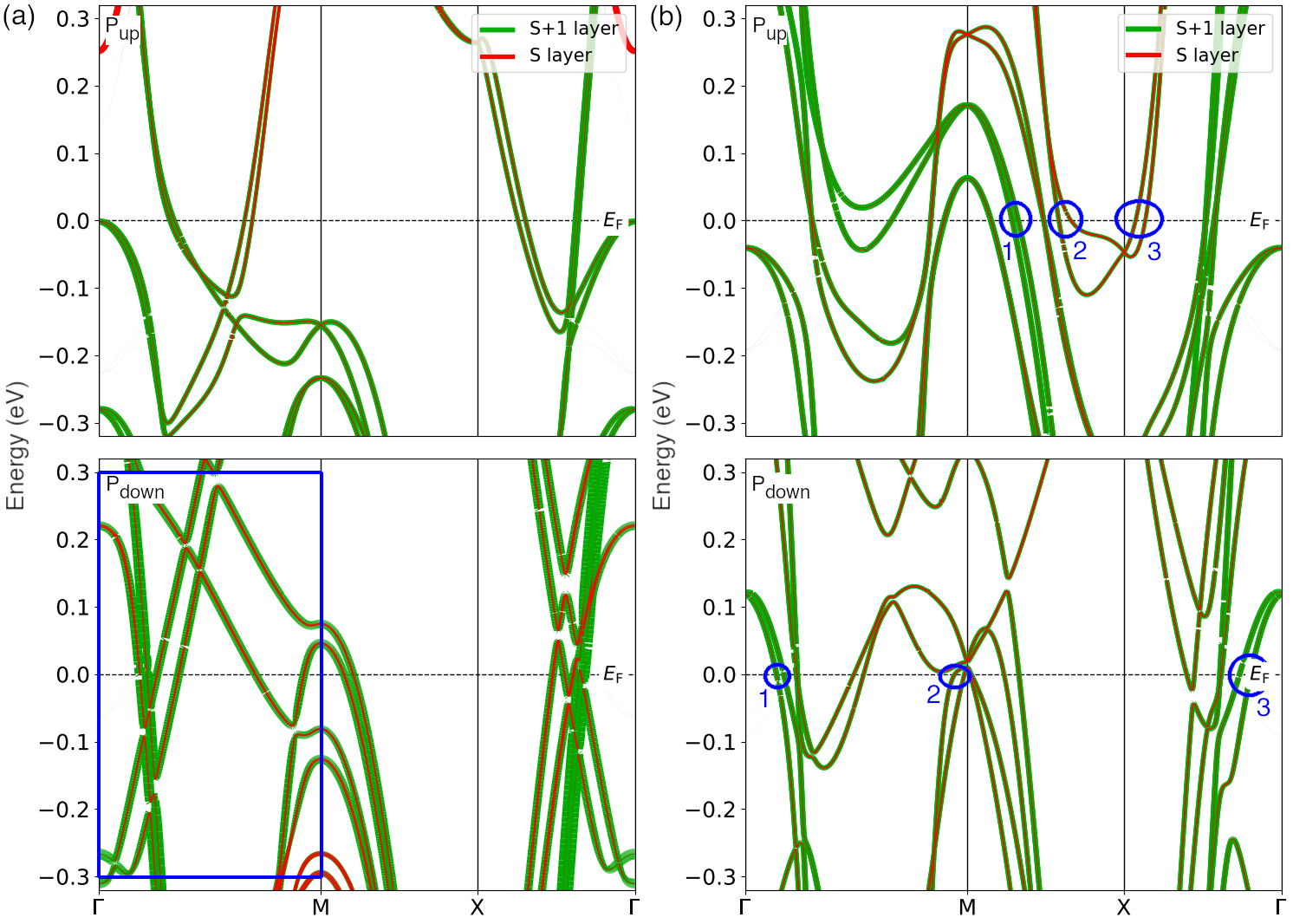
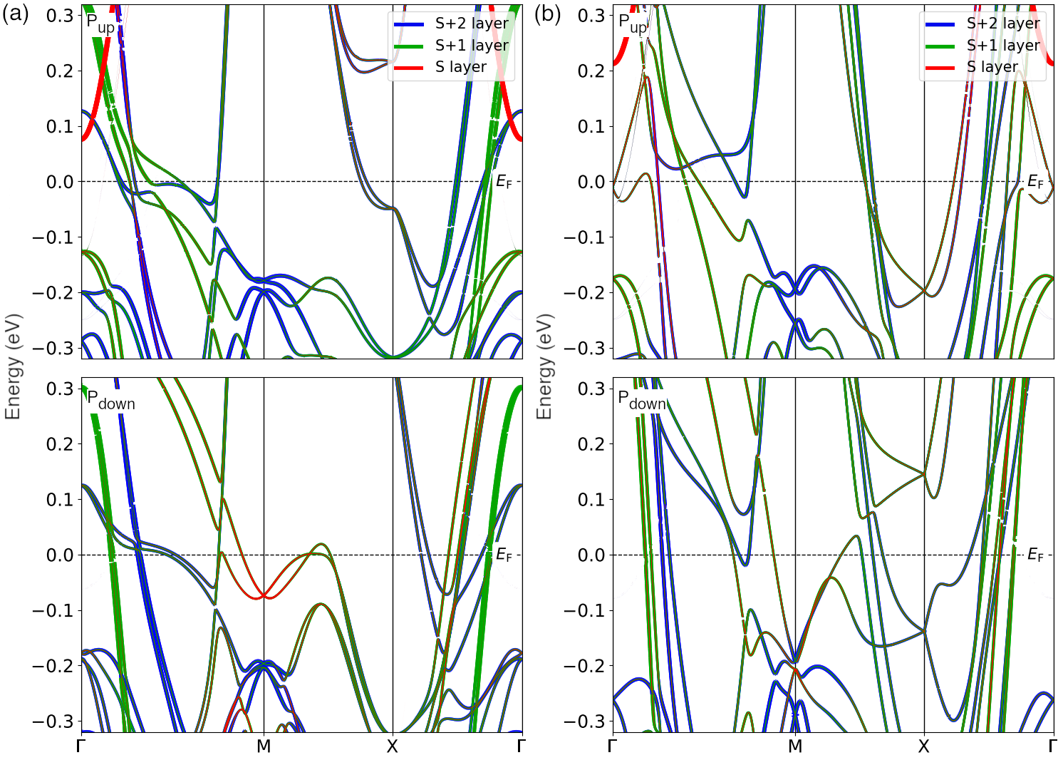
Further analysis of 2DEG can be made by plotting the layer-projected band structure near . We start from the case of 1ML Pd/PTO shown in Fig. 8 (a), in two panels of which the dispersion curves are plotted for each between eV and eV along the high symmetry directions of the Brillouin zone (BZ) within its plane. Importantly, all bands which cross belong to the Pd layer S+1 and interfacial Ti-O2 layer S. For the polarization state P, the Fermi surface (FS) seems relatively simple and includes a small isotropic hole sheet seen around the BZ center and the two double electron lenses situated in BZ along [100] between and X and along [110] between and M. When electric polarization of PTO is P the Fermi surface topology changes radically. This is shown in the lower panel of Fig. 8 (a). The -centered Fermi sheet disappears. Instead, a complicated multiple Fermi sheet object appears around the -point M (110). The multiple electron lenses, seen between and X and also between and M, change seriously in size and shape. Besides, few additional Fermi sheets appear here.
Although Pd and Pt are isoelectronic metals, the band structure of 1ML Pt/PTO plotted in Fig. 8 (b) differs from that of 1ML Pd/PTO. In general, the Pt overlayer S+1 provides more bands crossing , compared to the case of Pd. For both polarizations P and P, there are bunches of electronic branches which appear around each high-symmetry point of the BZ that may open extra channels for carriers. Hence, the 2DEG of Pt/PTO should be considered as more suitable for the charge transfer. The reversal of polarization indicates numerous qualitative changes of FS, while some of them represent the electronic topological transitions followed by valuable changes in the effective mass. Additionally, we calculated the band structure of 1ML Pt/PTO using the semi-infinite setup of dually polar PTO(001). After relaxation the calculated band structure changes marginally, as compared to the use of the 5-u.c.-thick PTO.
The second overlayer grown on PTO(001) yields more bands which cross . The corresponding band structures of 2ML Pd/PTO and 2ML Pt/PTO are shown in Figs. 9 (a) and 9 (b), respectively. As one can assume, there are notable differences in the FS topology and effective masses emerged due to the -reversal. Here, all band structures are plotted as non spin-polarized. This is because the magnetic moments induced on Pd and Pt and discussed above, as the result of interplay between the open surface and polar interface, may be suppressed by growing the next ferromagnetic overlayer on /PTO. Thus, we do not focus on spin polarization of 2DEG.
The SOC effect, however, needs to be analyzed more detailed. [58] We picked out for that the case of 1ML Pt/PTO, the band structure of which is plotted in Fig. 8 (b). Some selected Rashba splittings of the Pt bands seen near are enumerated in Fig. 8 (b) separately for P and P. This means that the two splitted bands, which are labeled by ”1” for P, differ completely from the P case. This is simply because the polarization reversal shifts the whole band structure far away from by 0.4 eV. For a better visualization of the Rashba SOC of 1ML Pt/PTO, we plot in Fig. 7 its band structure, which was calculated more accurately using the semi-infinite set up. One can easily detect the Rashba -splittings () at . The corresponding values are collected in Tab. 2. The typical SOC splittings selected for visualization do not exceed the value of 0.08 (1/Å). For each of the two splitted branches and for each polarization, we calculated their Fermi velocities. In general, these electron velocities range widely between 0.3 m/s and 4.1 m/s.
However, the velocities of splitted branches differ less significantly. In the case P and Rashba splitting labeled by ’3’ in Fig. 8 (b), the two splitted branches show velocities of 2.8 m/s and 3.7 m/s, whereas the case ’2’ for P gives 1.3 m/s and 2.0 m/s.
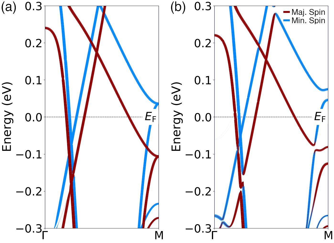
So far, we discussed the band structure and related Rashba splittings without taking into account their spin imbalance. This is because robustly induced spin polarization in the 2DEG should be considered quantitatively using ferromagnetic overlayer needed to complete the Edelstein effect. The SOC and broken inversion symmetry at the 2DEG interface affects the band structure and its spin polarization more seriously than ordinary Rashba splitting. In Fig. 10 we plot the spin-projected band structure of 1ML Pd/PTO calculated with and without the SOC. For a better comparison, one BZ direction –M and the case of P are shown there. These calculations were performed allowing for a noncollinear spintexture but keeping the spin angle that freezes the noncollinear degrees of freedom. One can see from Fig. 10 that for some branches the SOC changes both topology and spin polarization. This may affect the spin transport properties. Thus, a combination of SOC and spin degrees of freedom within the first-principles calculations opens a way to simulate nontrivial spin textures.
III.3 Transport via 2DEG
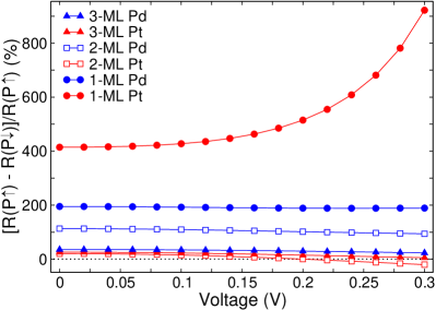
The steady-state transport calculations are performed using the QuantumATK package [52]. For this we used a -point grid while we kept the density mesh cutoff of 280 Ry as well as the broadening of 25 meV and the pseudopotentials. Afterwards we calculated the linear response current-voltage () characteristics by integrating the transmission spectrum for an applied bias between V and V. Therefor we applied the Landauer-Büttiker formalism [59] . The transmission coefficient depends on the spin , the energy , and the applied bias voltage . For the calculation of we applied a -point grid. Details of the application of this method are provided in Refs. [60, 61, 62]. The calculated current-voltage () characteristics of /PTO were used to calculate the resistance of each system which shows notable dependence on the PTO polarization state. Below, we discuss the case of Pd/PTO and Pt/PTO ( 1, 2, 3 ML), which (P) and (P) were used to obtain [(P) - (P)] between V and V. For each Pd, Pt and each , except for 1ML Pt/PTO, the stays almost constant over the voltage range which is not surprising (see Fig. 11). However, above 0.18 V, the assumption that the transmission is bias-independent seems invalid. We anticipate that the reversal of polarization in the PTO substrate changes the electroresistance of ultrathin metal overlayers by several percent.
IV Summary
We presented ab initio calculations of ferroelectrically controlled 2DEG and related Rashba splittings in ()/PbTiO3(001) ( Pd, Pt and 1, 2, 3 ML). Using the reliable computational set up to mimic the semi-infinite FE substrate, we performed systematic calculations which show how the band structure and its Rashba splitting differ in the Pt and Pd overlayers and how these electronic features change with increasing the metal thickness and reversal of electric polarization. From the basis of our calculations, one can conclude that platinum overlayers should be more suitable for the Rashba-Edelstein effect due to much stronger SOC and several electronic topological transitions occurring under the P-reversal. We anticipate the 20 % change in electroresistance of Pt/PTO upon the P-reversal that is a sizable value to attract extensive attention. These findings can stimulate further experimental and theoretical studies of high spin-to-charge conversion efficiency.
Recently, T. Kawada et al. have shown that the lattice displacements, excited by the surface acoustic waves in nonmagnetic layer of nonmagnetic/ferromagnetic metallic bilayers grown on piezoelectric substrate LiNbO3, including those of Pt/CoFeB and Pt/NiFe, facilitate a spin current [63]. The latter flows orthogonally to the propagation direction of acoustic waves, while acoustic voltage scales with the square of the spin Hall angle of nonmagnetic layer and is proportional to the acoustic wave frequency. Since PTO also possesses piezoelectricity, we suggest that Pt/PTO and Pd/PTO covered by CoFeB or NiFe may disclose the acoustic spin Hall effect which facilitate the the spin current and spin–charge conversion that is the forefront of advanced spintronics.
V Acknowledgments
Funding by the European Union (EFRE) via Grant No. ZS/2016/06/79307 and the Deutsche Forschungsgemeinschaft (DFG) via SFB CRC/TRR 227 is gratefully acknowledged.
References
- Lorenz et al. [2016] M. Lorenz, M. S. R. Rao, T. Venkatesan, E. Fortunato, P. Barquinha, R. Branquinho, D. Salgueiro, R. Martins, E. Carlos, A. Liu, F. K. Shan, M. Grundmann, H. Boschker, J. Mukherjee, M. Priyadarshini, N. DasGupta, D. J. Rogers, F. H. Teherani, E. V. Sandana, P. Bove, et al., The 2016 oxide electronic materials and oxide interfaces roadmap, J. Phys. D: Appl. Phys. 49, 433001 (2016).
- Ohtomo and Hwang [2004] A. Ohtomo and H. Y. Hwang, A high-mobility electron gas at the LaAlO3/SrTiO3 heterointerface, Nature 427, 423 (2004).
- Li et al. [2015] C. Li, Z. Liu, W. Lü, X. R. Wang, A. Annadi, Z. Huang, S. Zeng, and T. Venkatesan, Tailoring the Two Dimensional Electron Gas at Polar ABO3/SrTiO3 Interfaces for Oxide Electronics, Sci. Rep. 5, 13314 (2015).
- Xu et al. [2017] P. Xu, W. Han, P. M. Rice, J. Jeong, M. G. Samant, K. Mohseni, H. L. Meyerheim, S. Ostanin, I. V. Maznichenko, I. Mertig, E. K. U. Gross, A. Ernst, and S. S. P. Parkin, Reversible Formation of 2D Electron Gas at the LaFeO3/SrTiO3 Interface via Control of Oxygen Vacancies, Adv. Mater. 29, 1604447 (2017), 1604447.
- Stemmer and Allen [2014] S. Stemmer and S. J. Allen, Two-Dimensional Electron Gases at Complex Oxide Interfaces, Annu. Rev. Mater. Res. 44, 151 (2014).
- Maznichenko et al. [2020] I. V. Maznichenko, S. Ostanin, A. Ernst, J. Henk, and I. Mertig, Formation and Tuning of 2D Electron Gas in Perovskite Heterostructures, Phys. Status Solidi B 257, 1900540 (2020).
- Reyren et al. [2007] N. Reyren, S. Thiel, A. D. Caviglia, L. F. Kourkoutis, G. Hammerl, C. Richter, C. W. Schneider, T. Kopp, A.-S. Rüetschi, D. Jaccard, M. Gabay, D. A. Muller, J.-M. Triscone, and J. Mannhart, Superconducting Interfaces Between Insulating Oxides, Science 317, 1196 (2007).
- Hurand et al. [2015] S. Hurand, A. Jouan, C. Feuillet-Palma, G. Singh, J. Biscaras, E. Lesne, N. Reyren, A. Barthélémy, M. Bibes, J. E. Villegas, C. Ulysse, X. Lafosse, M. Pannetier-Lecoeur, S. Caprata, M. Grilli, J. Lesueur, and N. Bergeal, Field-effect control of superconductivity and Rashba spin-orbit coupling in top-gated LaAlO3/SrTiO3 devices, Sci. Rep. 5, 12751 (2015).
- Singh et al. [2018] G. Singh, A. Jouan, L. Benfatto, F. Couëdo, P. Kumar, A. Dogra, R. C. Budhani, S. Caprara, M. Grilli, E. Lesne, A. Barthélémy, M. Bibes, C. Feuillet-Palma, J. Lesueur, and N. Bergeal, Competition between electron pairing and phase coherence in superconducting interfaces, Nat. Commun. 9, 407 (2018).
- Park et al. [2020] D.-S. Park, A. D. Rata, I. V. Maznichenko, S. Ostanin, Y. L. Gan, S. Agrestini, G. J. Rees, M. Walker, J. Li, J. Herrero-Martin, G. Singh, Z. Luo, A. Bhatnagar, Y. Z. Chen, V. Tileli, P. Muralt, A. Kalaboukhov, I. Mertig, K. Dörr, A. Ernst, and N. Pryds, The emergence of magnetic ordering at complex oxide interfaces tuned by defects, Nat. Commun. 11, 3650 (2020).
- Santander-Syro et al. [2011] A. F. Santander-Syro, O. Copie, T. Kondo, F. Fortuna, S. Pailhes, R. Weht, X. G. Qiu, F. Bertran, A. Nicolaou, A. Taleb-Ibrahimi, P. Le Févre, G. Herranz, M. Bibes, N. Reyren, Y. Apertet, P. Lecoeur, A. Barthélémy, and M. J. Rozenberg, Two-dimensional electron gas with universal subbands at the surface of SrTiO3, Nature 469, 189 (2011).
- Bréhin et al. [2020] J. Bréhin, F. Trier, L. M. Vicente-Arche, P. Hemme, P. Noël, M. Cosset-Chéneau, J.-P. Attané, L. Vila, A. Sander, Y. Gallais, A. Sacuto, B. Dkhil, V. Garcia, S. Fusil, A. Barthélémy, M. Cazayous, and M. Bibes, Switchable two-dimensional electron gas based on ferroelectric Ca:, Phys. Rev. Materials 4, 041002(R) (2020).
- Vicente-Arche et al. [2021] L. M. Vicente-Arche, S. Mallik, M. Cosset-Cheneau, P. Noël, D. C. Vaz, F. Trier, T. A. Gosavi, C.-C. Lin, D. E. Nikonov, I. A. Young, A. Sander, A. Barthélémy, J.-P. Attané, L. Vila, and M. Bibes, Metal/ two-dimensional electron gases for spin-to-charge conversion, Phys. Rev. Materials 5, 064005 (2021).
- Bychkov and Rashba [1984] Y. A. Bychkov and É. I. Rashba, Properties of a 2D electron gas with lifted spectral degeneracy, JETP Lett. 39, 78 (1984).
- Caviglia et al. [2010] A. D. Caviglia, M. Gabay, S. Gariglio, N. Reyren, C. Cancellieri, and J.-M. Triscone, Tunable Rashba Spin-Orbit Interaction at Oxide Interfaces, Phys. Rev. Lett. 104, 126803 (2010).
- Vaz et al. [2019] D. C. Vaz, P. Noël, A. Johansson, B. Göbel, F. Y. Bruno, G. Singh, S. Mckeown-Walker, F. Trier, L. M. Vicente-Arche, A. Sander, S. Valencia, P. Bruneel, M. Vivek, M. Gabay, N. Bergeal, F. Baumberger, H. Okuno, A. Barthélémy, A. Fert, L. Vila, et al., Mapping spincharge conversion to the band structure in a topological oxide two-dimensional electron gas, Nat. Mater. 18, 1187 (2019).
- Noël et al. [2020] P. Noël, F. Trier, L. M. Vicente Arche, J. Bréhin, D. C. Vaz, V. Garcia, S. Fusil, A. Barthélémy, L. Vila, M. Bibes, and J.-P. Attané, Non-volatile electric control of spincharge conversion in a SrTiO3 Rashba system, Nature 580, 483 (2020).
- Edelstein [1990] V. M. Edelstein, Spin polarization of conduction electrons induced by electric current in two-dimensional asymmetric electron systems, Solid State Commun. 73, 233 (1990).
- Kondou et al. [2016] K. Kondou, R. Yoshimi, A. Tsukazaki, Y. Fukuma, J. Matsuno, K. S. Takahashi, M. Kawasaki, Y. Tokura, and Y. Otani, Fermi-level-dependent charge-to-spin current conversion by Dirac surface states of topological insulators, Nat. Phys. 12, 1027 (2016).
- Sánchez et al. [2013] J. C. R. Sánchez, L. Vila, G. Desfonds, S. Gambarelli, J. P. Attané, J. M. De Teresa, C. Magén, and A. Fert, Spin-to-charge conversion using Rashba coupling at the interface between non-magnetic materials, Nat. Commun. 4, 2944 (2013).
- Manipatruni et al. [2019] S. Manipatruni, D. E. Nikonov, C.-C. Lin, T. A. Gosavi, H. Liu, B. Prasad, Y.-L. Huang, E. Bonturim, R. Ramesh, and I. A. Young, Scalable energy-efficient magnetoelectric spinorbit logic, Nature 565, 35 (2019).
- Lesne et al. [2016] E. Lesne, Y. Fu, S. Oyarzun, J. C. Rojas-Sánchez, D. Vaz, H. Naganuma, G. Sicoli, J.-P. Attané, M. Jamet, E. Jacquet, J.-M. George, A. Barthélémy, H. Jaffrés, A. Fert, M. Bibes, and L. Vila, Highly efficient and tunable spin-to-charge conversion through Rashba coupling at oxide interfaces, Nat. Mater. 15, 1261 (2016).
- Vaz et al. [2018] D. C. Vaz, A. Barthélémy, and M. Bibes, Oxide spin-orbitronics: New routes towards low-power electrical control of magnetization in oxide heterostructures, Jpn. J. Appl. Phys. 57, 0902A4 (2018).
- Trier et al. [2020] F. Trier, D. C. Vaz, P. Bruneel, P. Noël, A. Fert, L. Vila, J.-P. Attané, A. Barthélémy, M. Gabay, H. Jaffrès, and M. Bibes, Electric-Field Control of Spin Current Generation and Detection in Ferromagnet-Free SrTiO3-Based Nanodevices, Nano Lett. 20, 395 (2020).
- Vaz et al. [2020] D. C. Vaz, F. Trier, A. Dyrdał, A. Johansson, K. Garcia, A. Barthélémy, I. Mertig, J. Barnaś, A. Fert, and M. Bibes, Determining the Rashba parameter from the bilinear magnetoresistance response in a two-dimensional electron gas, Phys. Rev. Materials 4, 071001(R) (2020).
- Dang et al. [2020] T. H. Dang, J. Hawecker, E. Rongione, G. Baez Flores, D. Q. To, J. C. Rojas-Sanchez, H. Nong, J. Mangeney, J. Tignon, F. Godel, S. Collin, P. Seneor, M. Bibes, A. Fert, M. Anane, J.-M. George, L. Vila, M. Cosset-Cheneau, D. Dolfi, R. Lebrun, et al., Ultrafast spin-currents and charge conversion at 3d-5d interfaces probed by time-domain terahertz spectroscopy, Appl. Phys. Rev. 7, 041409 (2020).
- Johansson et al. [2021] A. Johansson, B. Göbel, J. Henk, M. Bibes, and I. Mertig, Spin and orbital Edelstein effects in a two-dimensional electron gas: Theory and application to interfaces, Phys. Rev. Research 3, 013275 (2021).
- Mirhosseini et al. [2010] H. Mirhosseini, I. V. Maznichenko, S. Abdelouahed, S. Ostanin, A. Ernst, I. Mertig, and J. Henk, Toward a ferroelectric control of Rashba spin-orbit coupling: Bi on from first principles, Phys. Rev. B 81, 073406 (2010).
- Meyerheim et al. [2011] H. L. Meyerheim, F. Klimenta, A. Ernst, K. Mohseni, S. Ostanin, M. Fechner, S. Parihar, I. V. Maznichenko, I. Mertig, and J. Kirschner, Structural Secrets of Multiferroic Interfaces, Phys. Rev. Lett. 106, 087203 (2011).
- Guo et al. [2021] R. Guo, L. Tao, M. Li, Z. Liu, W. Lin, G. Zhou, X. Chen, L. Liu, X. Yan, H. Tian, E. Y. Tsymbal, and J. Chen, Interface-engineered electron and hole tunneling, Sci. Adv. 7, eabf1033 (2021).
- Quindeau et al. [2015] A. Quindeau, V. Borisov, I. Fina, S. Ostanin, E. Pippel, I. Mertig, D. Hesse, and M. Alexe, Origin of tunnel electroresistance effect in -based multiferroic tunnel junctions, Phys. Rev. B 92, 035130 (2015).
- Kurasawa and Mclntyre [2005] M. Kurasawa and P. C. Mclntyre, Surface passivation and electronic structure characterization of PbTiO3 thin films and Pt/PbTiO3 interfaces, J. Appl. Phys. 97, 104110 (2005).
- Fechner et al. [2008a] M. Fechner, S. Ostanin, and I. Mertig, Effect of the surface polarization in polar perovskites studied from first principles, Phys. Rev. B 77, 094112 (2008a).
- Garcia et al. [2010] V. Garcia, M. Bibes, L. Bocher, S. Valencia, F. Kronast, A. Crassous, X. Moya, S. Enouz-Vedrenne, A. Gloter, D. Imhoff, C. Deranlot, N. D. Mathur, S. Fusil, K. Bouzehouane, and A. Barthélémy, Ferroelectric Control of Spin Polarization, Science 327, 1106 (2010).
- Pantel et al. [2012] D. Pantel, S. Goetze, D. Hesse, and M. Alexe, Reversible electrical switching of spin polarization in multiferroic tunnel junctions, Nat. Mater. 11, 289 (2012).
- Duan et al. [2006] C.-G. Duan, S. S. Jaswal, and E. Y. Tsymbal, Predicted Magnetoelectric Effect in Multilayers: Ferroelectric Control of Magnetism, Phys. Rev. Lett. 97, 047201 (2006).
- Velev et al. [2009] J. P. Velev, C.-G. Duan, J. Burton, A. Smogunov, M. K. Niranjan, E. Tosatti, S. Jaswal, and E. Y. Tsymbal, Magnetic Tunnel Junctions with Ferroelectric Barriers: Prediction of Four Resistance States from First Principles, Nano Lett. 9, 427 (2009).
- Fechner et al. [2008b] M. Fechner, I. V. Maznichenko, S. Ostanin, A. Ernst, J. Henk, P. Bruno, and I. Mertig, Magnetic phase transition in two-phase multiferroics predicted from first principles, Phys. Rev. B 78, 212406 (2008b).
- Fechner et al. [2010] M. Fechner, I. V. Maznichenko, S. Ostanin, A. Ernst, J. Henk, and I. Mertig, Ab initio study of magnetoelectricity in composite multiferroics, Phys. Status Solidi B 247, 1600 (2010).
- Borek et al. [2012] S. Borek, I. V. Maznichenko, G. Fischer, W. Hergert, I. Mertig, A. Ernst, S. Ostanin, and A. Chassé, First-principles calculation of x-ray absorption spectra and x-ray magnetic circular dichroism of ultrathin Fe films on BaTiO3(001), Phys. Rev. B 85, 134432 (2012).
- Borisov et al. [2014] V. S. Borisov, S. Ostanin, I. V. Maznichenko, A. Ernst, and I. Mertig, Magnetoelectric properties of the (001) interface studied from first principles, Phys. Rev. B 89, 054436 (2014).
- Borisov et al. [2015] V. S. Borisov, S. Ostanin, S. Achilles, J. Henk, and I. Mertig, Spin-dependent transport in a multiferroic tunnel junction: Theory for , Phys. Rev. B 92, 075137 (2015).
- Liu et al. [2016] X. Liu, J. D. Burton, and E. Y. Tsymbal, Enhanced Tunneling Electroresistance in Ferroelectric Tunnel Junctions due to the Reversible Metallization of the Barrier, Phys. Rev. Lett. 116, 197602 (2016).
- Borisov et al. [2017] V. Borisov, S. Ostanin, and I. Mertig, Multiferroic properties of the PbTiO3/La2/3Sr1/3MnO3 interface studied from first principles, J. Phys. Condens. Matter 29, 175801 (2017).
- Li et al. [2017] T. Li, P. Sharma, A. Lipatov, H. Lee, J.-W. Lee, M. Y. Zhuravlev, T. R. Paudel, Y. A. Genenko, C.-B. Eom, E. Y. Tsymbal, A. Sinitskii, and A. Gruverman, Polarization-Mediated Modulation of Electronic and Transport Properties of Hybrid MoSBaTiOSrRuO3 Tunnel Junctions, Nano Lett. 17, 922 (2017).
- Umeno et al. [2009] Y. Umeno, J. M. Albina, B. Meyer, and C. Elsässer, Ab initio calculations of ferroelectric instability in capacitors with symmetric and asymmetric electrode layers, Phys. Rev. B 80, 205122 (2009).
- Velev et al. [2007] J. P. Velev, C.-G. Duan, K. D. Belashchenko, S. S. Jaswal, and E. Y. Tsymbal, Effect of Ferroelectricity on Electron Transport in Tunnel Junctions, Phys. Rev. Lett. 98, 137201 (2007).
- Meyerheim et al. [2013] H. L. Meyerheim, A. Ernst, K. Mohseni, I. V. Maznichenko, J. Henk, S. Ostanin, N. Jedrecy, F. Klimenta, J. Zegenhagen, C. Schlueter, I. Mertig, and J. Kirschner, Tuning the Structure of Ultrathin Films on Me(001) (, Pd, Pt) Surfaces, Phys. Rev. Lett. 111, 105501 (2013).
- Yang et al. [2020] Y. Yang, M. Wu, X. Li, H. Hu, Z. Jiang, Z. Li, X. Hao, C. Zheng, X. Lou, S. J. Pennycook, and Z. Wen, The Role of Ferroelectric Polarization in Resistive Memory Properties of Metal/Insulator/Semiconductor Tunnel Junctions: A Comparative Study, ACS Appl. Mater. Interfaces 12, 32935 (2020).
- Al-Saidi and Rappe [2010] W. A. Al-Saidi and A. M. Rappe, Density functional study of PbTiO3 nanocapacitors with Pt and Au electrodes, Phys. Rev. B 82, 155304 (2010).
- Kresse and Furthmüller [1996] G. Kresse and J. Furthmüller, Efficient iterative schemes for ab initio total-energy calculations using a plane-wave basis set, Phys. Rev. B 54, 11169 (1996).
- Smidstrup et al. [2017] S. Smidstrup, D. Stradi, J. Wellendorff, P. A. Khomyakov, U. G. Vej-Hansen, M.-E. Lee, T. Ghosh, E. Jónsson, H. Jónsson, and K. Stokbro, First-principles Green’s-function method for surface calculations: A pseudopotential localized basis set approach, Phys. Rev. B 96, 195309 (2017).
- Perdew et al. [1996] J. P. Perdew, K. Burke, and M. Ernzerhof, Generalized Gradient Approximation Made Simple, Phys. Rev. Lett. 77, 3865 (1996).
- Van Setten et al. [2018] M. Van Setten, M. Giantomassi, E. Bousquet, M. J. Verstraete, D. R. Hamann, X. Gonze, and G.-M. Rignanese, The PseudoDojo: Training and grading a 85 element optimized norm-conserving pseudopotential table, Comput. Phys. Commun. 226, 39 (2018).
- Anisimov et al. [1991] V. I. Anisimov, J. Zaanen, and O. K. Andersen, Band theory and Mott insulators: Hubbard U instead of Stoner I, Phys. Rev. B 44, 943 (1991).
- Anisimov et al. [1993] V. I. Anisimov, I. V. Solovyev, M. A. Korotin, M. T. Czyżyk, and G. A. Sawatzky, Density-functional theory and NiO photoemission spectra, Phys. Rev. B 48, 16929 (1993).
- Solovyev et al. [1994] I. V. Solovyev, P. H. Dederichs, and V. I. Anisimov, Corrected atomic limit in the local-density approximation and the electronic structure of d impurities in Rb, Phys. Rev. B 50, 16861 (1994).
- Varignon et al. [2019] J. Varignon, J. Santamaria, and M. Bibes, Electrically Switchable and Tunable Rashba-Type Spin Splitting in Covalent Perovskite Oxides, Phys. Rev. Lett. 122, 116401 (2019).
- Büttiker et al. [1985] M. Büttiker, Y. Imry, R. Landauer, and S. Pinhas, Generalized many-channel conductance formula with application to small rings, Phys. Rev. B 31, 6207 (1985).
- Brandbyge et al. [2002] M. Brandbyge, J.-L. Mozos, P. Ordejón, J. Taylor, and K. Stokbro, Density-functional method for nonequilibrium electron transport, Phys. Rev. B 65, 165401 (2002).
- Taylor et al. [2001] J. Taylor, H. Guo, and J. Wang, Ab initio modeling of open systems: Charge transfer, electron conduction, and molecular switching of a device, Phys. Rev. B 63, 121104(R) (2001).
- Soler et al. [2002] J. M. Soler, E. Artacho, J. D. Gale, A. García, J. Junquera, P. Ordejón, and D. Sánchez-Portal, The SIESTA method for ab initio order- materials simulation, J. Phys.: Condens. Matter 14, 2745 (2002).
- Kawada et al. [2021] T. Kawada, M. Kawaguchi, T. Funato, H. Kohno, and M. Hayashi, Acoustic spin Hall effect in strong spin-orbit metals, Sci. Adv. 7, eabd9697 (2021).