Embedded Firmware Development for a Novel CubeSat Gamma-Ray Detector
Abstract
The Gamma-ray Module (GMOD) is an experiment designed for the detection of gamma-ray bursts in low Earth orbit as the principal scientific payload on a 2-U CubeSat, EIRSAT-1. GMOD comprises a cerium bromide scintillator coupled to silicon photomultipliers which are processed and digitised by a bespoke ASIC. Custom firmware on the GMOD motherboard has been designed, implemented and tested for the MSP430 microprocessor which manages the experiment including readout, storage and configuration of the system. The firmware has been verified in a series of experiments testing the response over a realistic range of input detector trigger frequencies from 50 Hz to 1 kHz for the primary time tagged event (TTE) data. The power consumption and ability of the firmware to successfully receive and transmit the packets to the on-board computer was investigated. The experiment demonstrated less than 1 % loss of packets up to 1 kHz for the standard transfer mode with the power not exceeding 31 mW. The transfer performance and power consumption demonstrated are within the required range of this CubeSat instrument.
Index Terms:
CubeSat, Gamma-ray, Detector, Gamma-ray Burst, European Space Agency Fly Your Satellite! ProgrammeI Introduction
The Gamma-Ray Module (GMOD) [1] is a novel instrument developed to study high energy astrophysical transient events called gamma-ray bursts (GRBs) [2] in the era of multi-messenger astronomy. GMOD will be flown in low earth orbit (LEO) on-board the Educational Irish Research Satellite-1 (EIRSAT-1), a 2U CubeSat developed as part of the European Space Agency (ESA) Fly Your Satellite! (FYS) programme[3]. The sustained miniaturisation of technology has been the driving force behind the development of CubeSats for science applications[4]; these are small satellites whose mass and dimensions are defined in units of “U” where 1U corresponds to a CubeSat of 10cm10cm10cm in volume and approximately 1.3kg in mass[5]. GMOD is a 1U scintillation based gamma-ray detecting instrument which features modern miniaturised detector technology in a robust and low power, CubeSat compatible form factor. The development of the GMOD detector builds on previous work including a number of technology investigations [6, 7], a five hour balloon flight at 37km float altitude [8], a 101.4MeV proton irradiation test [9] and most recently, the engineering qualification model environmental test campaign, including vibration and thermal-vacuum testing [10]. GMOD is expected to detect 11–14 GRBs over a one year mission at a significance of 10 , within the standard 50 keV to 300 keV energy range [11].
When complete, GMOD will be used as the basis for a scaled up configuration of CubeSat compatible gamma-ray detectors allowing localisation capabilities as part of the Gamma-Ray Investigation of the Full Transient Sky (GIFTS) project. GMOD and other CubeSat instruments can also be used to augment the observing capabilities of the current fleet of GRB detecting missions. These include large missions such as the Fermi Space Telescope[12], INTEGRAL[13], the Neil Gehrels Swift Telescope and planned CubeSat missions and small satellites such as BurstCube[14] and GECAM [15].
In 2017, a breakthrough discovery was made when GRB170817A, a coincident electromagnetic counterpart to GW170817, a gravitational wave (GW) event was detected [16, 17]. This coincident detection marked the beginning of a new era of multi-messenger astronomy and highlighted the importance of gamma-ray missions in the detection of coincident GW and GRB events, an effort which GMOD will contribute to as a member of the wider GRB community.
In addition to the science goals of detecting GRBs, GMOD will further the technology readiness of advanced detector technologies; including that of silicon photomultipliers (SiPMs) which are used to provide a compact, low power, and rugged solid state alternative to the larger, high-voltage and fragile photomultiplier tubes (PMTs), as used on earlier space borne gamma-ray detecting instruments. The GMOD detector will be functionally supported by a custom built readout and support system consisting of a motherboard (MB) which will provide a number of operation critical duties. This in-house developed system will accomplish this using a C/C++ firmware running on a Texas Instruments MSP430FR5994 mixed signal processor, a 16-bit, low power, 16 MHz microcontroller. We present an overview of the development of this firmware, the context of its requirements for satisfactory operation and an initial assessment of its performance to date with planned improvements and future work.
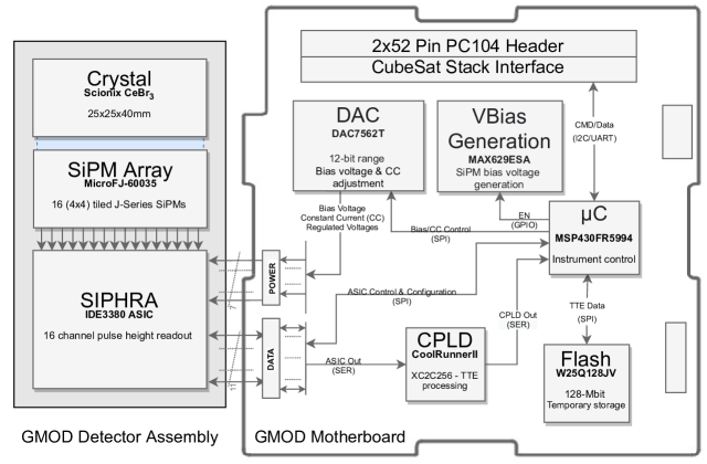
II The Gamma-ray Module
GMOD comprises a 25mm25mm40mm Scionix cerium bromide (CeBr3) scintillator which is optically coupled to a custom built tiled array of 16 (44) OnSemiconductor MicroFJ-60035-TSV SiPMs [1][3][11]. Front-end readout for the SiPM array is provided by the 16 channel IDE3380 SIPHRA application specific integrated circuit (ASIC), produced by IDEAS (Norway)[18, 19]. The ASIC was developed to be a readout solution for pulse height spectroscopy in instruments using SiPMs, PMTs or multi-pixel photon counters and is implemented as a bare silicon die wire-bonded to a carrier board printed circuit board (PCB). This detector assembly is sealed within a light-tight custom machined aluminium enclosure and bolted directly to the GMOD MB. The GMOD MB is a bespoke readout and support system for the GMOD detector assembly, providing a number of operation critical duties, including the generation of an adjustable SiPM bias voltage, a constant current source, system configuration, readout and the temporary on-board flash storage of individual gamma-ray time-tagged event (TTE) packets. This was developed over a number of demonstration model iterations to be both a tailored solution for the instruments readout and control, as well as to serve as a structural mounting point for the detector assembly hardware. A high level operational layout of the GMOD instrument is presented in Figure 1, while a component list is detailed in Table I.
Readout of the detector occurs as follows: a gamma-ray is either partially or fully absorbed by the CeBr3 scintillator, which in turn produces a number of photons proportional to the energy of the incident gamma-ray within a wavelength matching the peak photo sensitivity of the J-Series SiPM array. Each SiPM is made up of an array of many thousands of microcells, avalanche photodiodes in Geiger-mode operation with a series quench resistor; photons absorbed by these microcells trigger an avalanche flow releasing a fixed amount of charge which is proportional to the energy of the incident gamma-ray photon. SIPHRA integrates and shapes this current signal, which when surpassing a fixed trigger threshold, triggers digitisation of the pulse height using a 12-bit successive approximation register (SAR) analogue to digital converter (ADC). The ASIC then outputs the event data as a 20-bit serial stream at 1M Baud for each active SiPM channel, 12-bits for the ADC measurement and the remaining bits allocated to channel trigger information. This is an unusual form of serial transmission which cannot be readily handled by the MSP430 enhanced universal serial communication interface (eUSCI) module and must first be reduced for efficient bit packing. This is performed by a Xilinx XC2C256 Complex Programmable Logic Device (CPLD) which directly receives the SIPHRA trigger data and produces two types of TTE: 16 channel, containing measurements for each active SiPM channel and summed channel, containing the summed signal measurements from the SiPM array. The CPLD also applies a 4 byte fine-timestamp with a 1 s time base and an attached synchronous marker (ASM) as identification bytes for distinct recognition of the TTE type (as either summed channel or 16 channel data). It is at this point that both summed and 16 channel TTEs, consisting of the pulse height spectroscopic measurements from the detector, are transmitted to the MSP430FR5994 microcontroller over 1 MBaud serial for processing and temporary storage, before eventual transmission to the EIRSAT-1 on-board computer (OBC) [20].
According to simulations[11] performed using the The Medium-Energy Gamma-Ray Astronomy Library (MEGAlib) [21], GMOD is expected to have a background gamma-ray trigger rate of 50 Hz within the 50 - 300 keV energy range, and (possibly closer to 100 Hz in a wider energy band). GMOD is expected to detect between 11 and 14 GRBs over its one year mission at a significance of 10 , depending on spacecraft pointing[11]. This corresponds to a SIPHRA trigger rate of around 120 Hz over a single 1024 ms binned light curve record. It is not expected that GMOD will see GRBs which generate over 500 counts per second and the vast majority of GRB triggers will be less than 10 . In terms of the extreme, SIPHRA’s trigger rate in GMOD can just about exceed 1000 Hz, after which it is capped by the time it takes to output all active SiPM channel readout. An event triggering SIPHRA at such high rates for any long duration is not expected, however high rates are expected while transiting the South Atlantic Anomaly (SAA) (due to the concentration of high energy protons) or if passing through high latitude regions (due to the concentration of high energy electrons)
| Detector | ||||
| Crystal | Scionix CeBr3 252540mm | |||
| SiPM | OnSemiconductor MicroFJ60035-TSV | |||
| Array | Custom 4x4 (16) tiled SiPM array | |||
| Front-end | SIPHRA IDE3380 ASIC (Carrier Board) | |||
| Motherboard | ||||
| C | 16-bit, Texas Instruments MSP430FR5994 | |||
| CPLD | Xilinx CoolRunnerII XC2C256 | |||
| Storage | 128-Mbit (16 MB) temporary flash storage | |||
| DAC | 12-bit DAC7562T (bias/CC supply adjustment) | |||
| MSP430FR5994 Peripherals | ||||
| CPU | 16 MHz, 16-bit RISC architecture | Clk Sys | 3 independent clocks (MCLK, SMCLK, ACLK) | |
| FRAM | 256 kB storage | ADC | 12-bit SAR | |
| SRAM | 8 kB storage | GPIO | 68 multiplexed I/O | |
| DMA | 6 channels | CRC | 32-bit 16-bit CRC | |
| Timer | 6 16-bit timers with 7 CCRs | eUSCI | eUSCI_A (4SPI/UART), eUSCI_B (4SPI/I2C) | |
III The MSP430FR5994
At the core of this system is the Texas Instruments (TI) MSP430FR5994 [22] [23], a 16 MHz mixed signal microcontroller based on a reduced instruction set computer architecture. This device was selected for numerous reasons: its low-power optimisation, 256 kB of high speed ferroelectric random access memory (FRAM), a variety of integrated peripheral modules, past family space heritage[24] and ease of accessibility. The MSP430 can be placed into an number of operational states called “low power modes”, effectively a set of predefined states of activity which selectively enable or disable the central processing unit (CPU), peripheral modules and their relevant clock sources. The current consumption of any digital device is in general related to the rate at which it is clocked; the MSP430 clock system can produce three independently configurable clock signals for the CPU and peripherals. By varying the low power mode (LPM) setting certain clock sources and peripheral resources may be placed into a low power state while others remain active. This allows the user to develop a firmware which can optimise the current consumption of the device depending on the stage of operation. The combined use of LPM states and internal FRAM storage helps to reduce the power requirements of the MSP430. FRAM is equivalent to flash memory in terms of its interface and non-volatility, but superior in terms of read/write access (close to 8 MBps compared to flash at 14 kBps), read/write endurance (1015 write/erase cycles compared to 105 for flash)[25], and ultra-low-power requirements (requiring just 1.5V compared to 10-14V for the flash charge pump). It has even been shown to have some level of radiation resilience[26] and a reduced soft error rate (SER) [27] as compared to static random access memory (SRAM), 8 kB of which is available on the MSP430FR5994111This is partitioned in the default linker file provided by TI in Code Composer Studio (CCS), into 4 kB blocks, half allocated to common use by the CPU and stack, while the other reserved for the Low-Energy Accelerator module. As this is unused on GMOD, this has been merged into a single 8 kB block.. The device has a large selection of internal peripheral modules: six 16-bit timers with multiple capture compare registers, two eUSCI modules (eUSCI_A supporting up to 4 channels independently configurable as either UART/SPI and eUSCI_B supporting up to 4 channels independently configurable as either I2C/SPI), a 6 channel direct memory access (DMA) controller, a 12-bit SAR ADC with multiplexed inputs and 68 multiplexed general purpose input/outputs. These combined make the MSP430 a versatile option for the multiple requirements of GMOD and the general use of it in a variety of space applications. For example, the 430 platform of the MSP family has seen frequent use within CubeSat Kits[28, 29], small satellites[30][31] and CubeSat subsystems[32]. It was most notably used on the Mars Cube One (MarCO) [24] CubeSats, companions to the National Aeronautics and Space Administration (NASA) Interior Exploration using Seismic Investigations, Geodesy and Heat Transport (InSight) lander during its 2018 Martian arrival. Finally, a large resource of example code222https://www.ti.com/product/MSP430FR5994 has been made available by TI for the MSP family of devices, including the MSP430FR5994, which hosts both register level and driver level examples. A wealth of documentation and application notes are also available with detailed information on all aspects of the register configuration settings for device operation. This makes writing and testing firmware on the MSP430 an approachable task for CubeSat teams, many of which are composed of university level students, as is the case for EIRSAT-1.
A firmware specifically designed to take advantage of all of these qualities can provide high performance with a low power optimised operation. A preliminary C/C++ firmware has been developed for GMOD using the Eclipse based, TI CCS [33] integrated development environment (IDE). To date, the firmware has been verified in a series of experiments testing its response over a range of detector trigger frequencies. The power consumption and ability of the firmware to successfully process this data was investigated.
IV MSP430FR5994 Firmware Operation
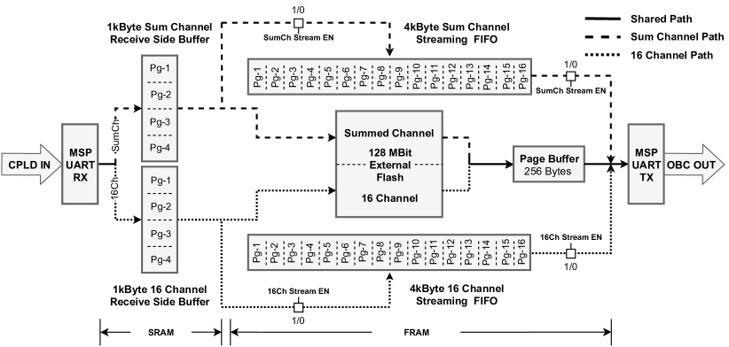
In summary, the firmware operation is such that TTE packets are recieved from the CPLD, are processed and then stored in external 128-Mbit flash for service to the OBC. The MSP430 manages this flash storage by dividing it into a pair of circular ring buffers of equal size (a separate partition for summed channel and 16 channel TTEs). Upon request from the OBC, these TTEs are retrieved by the MSP430 and served to the OBC for GRB triggering, light curve and spectra generation. The MSP430 may also “stream” the TTE data directly to the OBC from internal memory for improved data transmission (all TTE data is stored in flash in the event that streaming becomes desynchronised, in this case servicing must restart from the last expected address). The MSP430 is also responsible for other duties which include the configuration of the ASIC, CPLD reprogramming and enabling and controlling of the SiPM bias voltage and 80 A constant current supply (for internal ASIC biasing). As a contingency while in flight, it is possible for the MSP430 to reprogram the CPLD using Xilinx Serial Vector Format (XSVF) instructions and a software interpreter which decodes the commands into the required JTAG I/O stimulus[34]. For brevity, only the experiment operation will be examined here as represented in Figure 2.
The MSP430 receives TTE packets generated by the CPLD based on trigger data from the ASIC. Interrupts are generated by the designated MSP430 serial module at the reception of individual bytes from the CPLD. The MSP430 waits until a recognisable 2 byte ASM sequence has been received which identifies the type of incoming TTE and will determine the specific response actions for summed or 16 channel packets. Both summed and 16 channel data are handled separately within the MSP430 memory and external flash and must be individually requested by the OBC. This is because summed channel TTE packets are the primary science product of GMOD; all scientific operations for GRB triggering will be carried out using summed channel data within the OBC. 16 channel TTE packets are a secondary product and have limited utility except for use in technology demonstrations or in health check assessments of individual SiPM channels. In flight, the main mode of operation will likely not include 16 channel readout, but it may be enabled on occasion.
Once a recognised ASM has been received, the expected number of TTE serial bytes are read in and stored within a set of SRAM circular buffers in MSP430 memory. The TTEs are temporarily stored here before transmission to flash or before being queued for streaming. There are two of these “receive-side” buffers on the MSP430, one for summed channel data and one for 16 channel data, both of identical length (1 kB). Each circular buffer can contain up to 4 pages (4256 bytes, where 1 page = 256 bytes) of the given TTE data type. Each page can hold 31 summed channel TTEs or 7 16 channel TTEs. This difference is due to the larger number of bytes per 16 channel TTE as compared to summed channel TTEs, effectively meaning that the 16 channel receive-side buffer is 4 times smaller in terms of the number of TTEs which can be packed within each 256 byte page. For this reason, at high data rates, the 16 channel buffers are expected to fill faster than the summed channel buffers. If at any point a receive-side buffers fills completely, TTE data is no longer accepted for the given TTE type, until at least a page worth of the received side buffer has been emptied by transmission to flash storage (this is a temporary solution employed only for initial testing).
Once a full page of either TTE type has been received, it may be stored within flash memory. The receive side buffer may continue to be filled during the writing of data to flash. A state within the main loop is entered which primes the page for transmission to flash storage; the flash command and address bytes are prepended to the contiguously arranged TTE page bytes, a 4 byte coarse-timestamp is applied to the page with 1s time base, and for summed channel a cyclical redundancy check (CRC) is calculated (due to the lower priority status of 16 channel data, error detection is not considered beneficial for this data type and is excluded). The page is then transmitted to flash over 8 MHz SPI, using DMA to place each byte from SRAM memory into the SPI module transmit buffer. DMA transfer of data has been used extensively in the experiment firmware, where possible, in an attempt to optimise the transmission of large amounts of TTE data and to reduce the chance of bottlenecking at high trigger rates.
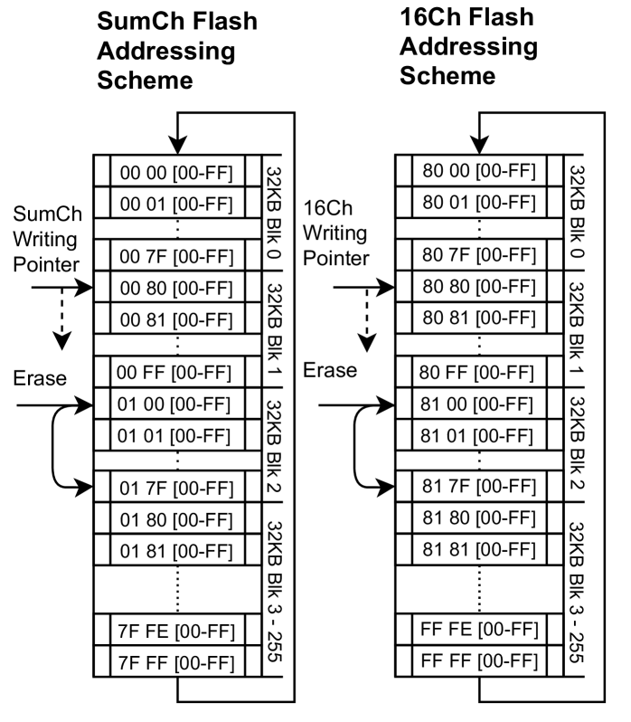
SRAM memory has been used for the receive-side buffer storage; while FRAM is more abundant on the MSP430FR5994, its read/write cycles are capped at 8 MHz333It is possible to improve the write speed of FRAM [25] access in conjunction with DMA transfers, something which is exploited in other areas of the MSP430 firmware. where as SRAM is limited only by the clock source which in the current configuration is set to 16 MHz. The use of SRAM helps to ensure data in the receive-side is transferred to external flash with minimum overhead. As with the receive-side buffers on the MSP430, the Winbond W25Q128JV 128-Mbit flash is partitioned in half, the upper address space being reserved for summed channel data while the lower range being reserved for 16 channel data, as in Figure 3. As the addressing for the flash is a 3 byte sequence, the boundaries between the two TTE data types can be easily identified by the firmware, using the most significant bit of the addressing to differentiate the summed channel range and the 16 channel range – this is useful as a simple bit mask can be used to prevent accidental pointer overflow. Each flash partition acts as an independent circular buffer, similar to the receive-side buffers in the MSP430 SRAM memory. In the case of the flash memory, a “writing pointer” for each buffer is recorded by the MSP430 which is an index of the address in flash to be written to next. This is as opposed to the conventional “head” and “tail” used in most circular buffers, which point to the start and end of the stored data respectively. The OBC can read this pointer and determine the amount of unread TTE pages in flash memory. It is important that the amount of unread data in flash which has yet to be transmitted to the OBC is kept as close to a minimum as possible to avoid the unlikely event that the flash buffer overflows and TTE data is overwritten. For the expected background rate of 50 Hz in LEO, the summed channel buffer will take 5.7 hours without reading to fill, with the 16 channel buffer filling within 1.2 hours without reading. As the memory capacity available is so large, particularly in the summed channel buffer memory space (which is to be used for GRB triggering), it is unlikely that the OBC will need to request data from address outside all but a narrow window of address space.
As flash memory is used as a circular buffer, the memory address space is cycled many times during the experiment operation. Once the TTE data has been written to flash and is no longer needed in storage, rewriting to this location requires a pre-erase of the memory location essentially priming it for subsequent write operations.
These erase operations take a considerable amount of time to complete (for example 45 ms for 4 kB sectors and 120 ms for a 32 kB block). When these erases are staged to occur in the MSP430 firmware, critical read/write operations to/from flash are blocked for this duration. Given these long erase times, it is possible that the receive-side buffers may overflow before the flash is available again for writing. Erases are therefore managed in a dynamic way by suspending flash erase operations to prioritise the writing of new TTE data to flash. Once the write has completed, the erase operation may then be resumed and continued in the background until completion. In the case of GMOD, erase operations are performed on a 32 kB block basis, one block ahead of the “write pointer” location (128 ms completion time). Thus the current block will have been cleared previously and be available for writing, while the following block has either been erased or is currently being erased, ensuring that there is always 32 kB of flash available for writing and only a minimal amount of stored data is erased and recycled for reuse. In this way, the erase of an addressed block of flash memory is triggered by proximity to the current “write pointer” address (ie. when writing to the start of a 32 kB block boundary, the next block is immediately staged to be cleared by erasing its contents for reuse, as illustrated in Figure 3). This strategy strikes a balance between maintaining as much historical TTE data in memory as possible while still ensuring that erases occur in a timely manner to allow new data to be successfully written.
When the OBC requests data from a given address it is retrieved from flash in pages and placed within MSP430 FRAM memory. This flash read operation is handled using DMA to read data from the eUSCI SPI receive buffer and load it into FRAM memory. A frame structure is applied to the page before sending to the OBC, with a header containing a unique 4 byte ASM sequence, identifying the start of the data frame and the flash address bytes from where the page originated. It is then transmitted to the OBC over 128 kBaud serial. Once the OBC receives the packet and confirms the address bytes are as expected, the next page may then be requested if available.
For a faster throughput of data from GMOD to the OBC, a streaming system has been developed which allows the MSP430 to serve TTE data from internal memory rather than fetching from external flash. It is expected that this will be the primary mode of data transfer from the MSP430 during operation. When the MSP430 transfers the TTE page to flash (and when the streaming mode is enabled), that same page is transferred to a larger 4 kB circular buffer which can hold 16 TTE pages. A pair of 4 kB “streaming” buffers are reserved in FRAM, one for summed channel data and another for 16 channel data. When a page has been loaded into either streaming buffer, it may be transmitted to the OBC. The OBC may then check the received address bytes in the packet frame to ensure that the correct page was sent by GMOD and that the data has been transmitted in the expected consecutive order according to the incriminating address bytes. If an inconsistency is detected between received TTE pages, the OBC may disable streaming and reenable streaming from the last expected page address in flash. The MSP430 then streams the contents directly from flash up from this address to the current “writing pointer” and the re-enables the streaming from internal memory at this point, whereupon subsequent pages are transmitted directly from the MSP430 FRAM. If these streaming buffers overflow, the MSP430 can proactively reenable streaming from flash memory to the current “writing pointer” and then reenable streaming directly from the MSP430 FRAM.
Within the main loop of the firmware application is a set of states which define GMOD’s operating configuration. At this stage of development, four distinct modes are defined, the two most relevant being Idle Mode, where GMOD may be configured but where the experiment is not currently active and Experiment Mode, similar to Idle Mode, except the experiment is currently running. The OBC may move GMOD between these different modes, which define certain configurations and the scope that the MSP430 can independently act within. To take full advantage of the low power optimisation on the MSP430, when GMOD is placed into Idle Mode, the MSP430 returns to a LPM-3 state (where the CPU is deactivated and the two high speed clock sources (out of three sources in total) have been disabled). In Experiment mode the MSP430 returns to a LPM-0 state (where both the CPU and its clock source are disabled). Deeper LPM states allow low power operations at the expense of functionality, speed and device wake up time. For instance, placing the MSP430 into LPM-0 while in Experiment Mode has the trade off of slightly higher power draw, while retaining the fast interrupt response and wake up time necessary for TTE collection.
V Initial Performance Analysis
A number of iterations of this firmware have been developed and tested. Initial testing using the current firmware, indicates that the MSP430 is capable of meeting the requirements of the GMOD instrument in terms of readout and storage, power consumption and data rate handling in the context of GRB detection. The developed firmware must be able to successfully meet the following minimum operating requirements in order to be considered successful:
-
•
Retention of all received TTEs from SIPHRA and the CPLD without loss or corruption.
-
•
Managing trigger rates up to at least 500 Hz for summed channel data (as this is used for GRB triggering).
-
•
Achieve Low power optimisation with firmware development – power must be less than 181.5 mW (exc. 30 margin) estimated consumption as defined in the spacecraft initial Design Definition File (DDF) [35].
This firmware was tested by externally triggering SIPHRA at a range of fixed trigger rates, intercepting the CPLD output and comparing it against the MSP430 output. This was done in two separate tests, a test where only the summed channel readout was enabled and the other where both the summed and 16 channel readout were enabled. The intention behind this was to investigate the effects of bottlenecking within the MSP430 during high data rates when both 16 channel and summed channel TTE readout was enabled, to determine the trigger rate at which this would begin and to assess how many summed TTEs would be lost as a result. Furthermore, it was expected the power consumption of the MSP430 and GMOD motherboard would increase with both summed and 16 channel readout being processed, as at high data rates the MSP430 is likely being kept in a sustained active state while the flash is being read and written to more often than when just summed channel data is being processed. For this test only the reception of summed channel data was examined given its higher priority for scientific operations as opposed to 16 channel data. 16 channel data was also received to adequately simulate a full readout, however the handling of this data is beyond the scope of these initial tests and is not discussed.
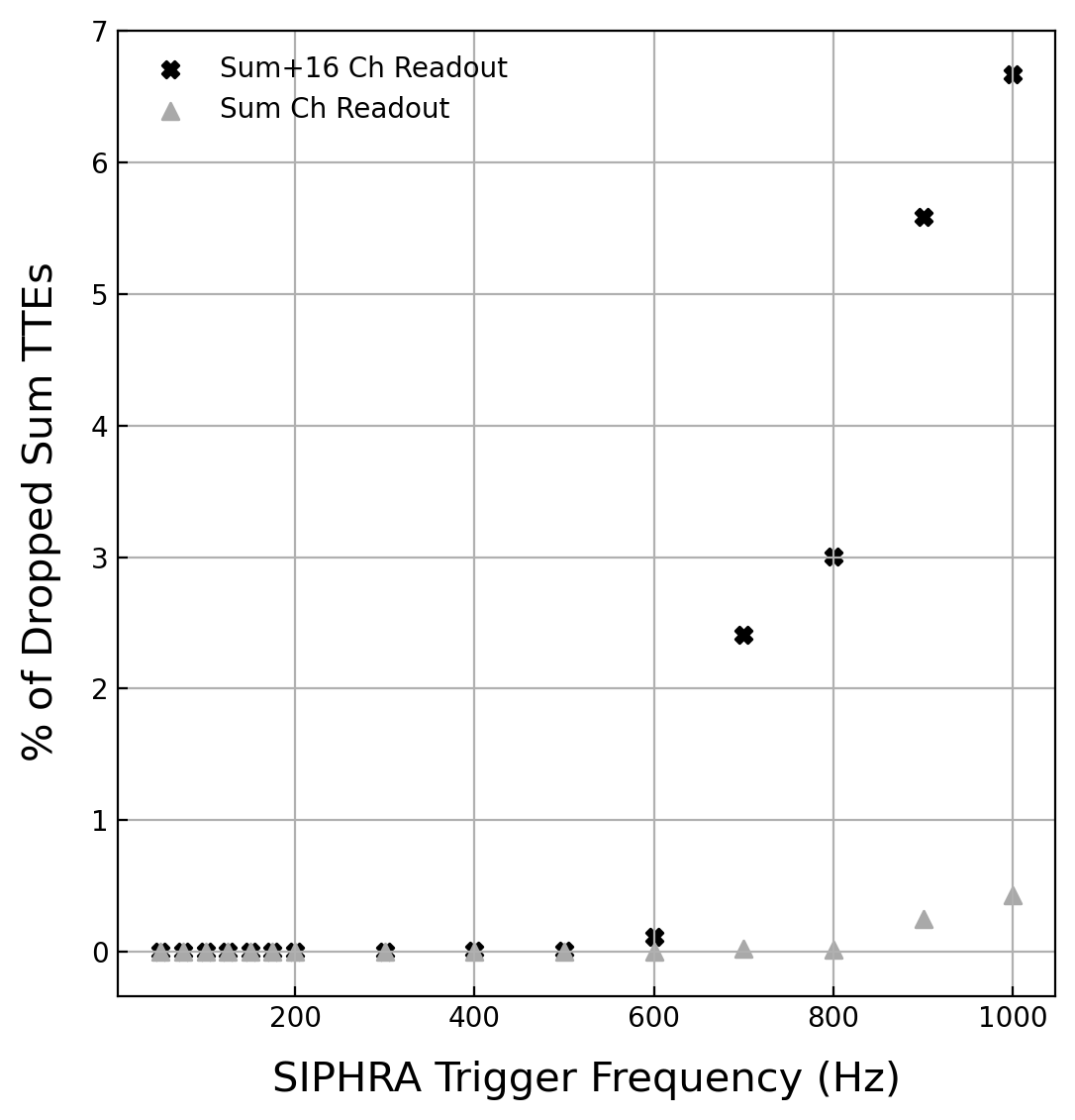
An external hold input for SIPHRA’s track and hold circuit is available, which when asserted, forces a readout which is processed by the CPLD and assigned a fine-timestamp as during normal operation. For this test, the hold signal was generated using the Aim-TTi TG5011 pulse generator, which was configured as a 3.3 V, 25 s pulse width output, across a frequency range spanning 50 Hz up to 1 kHz. For the purposes of this test, the detector assembly, with the exception of the SIPHRA ASIC, was not needed and was disconnected. A modified version of the CPLD VHDL was used to mirror the serial output to the MSP430 over an easily accessible GPIO pin which could be logged to a PC using an FTDI USB to serial adaptor. GMOD was placed into Experiment Mode and commanded to begin streaming TTE data which was similarly also logged using a second FTDI serial device. It was at this point that the readout configuration was set with streaming enabled (ie. summed channel readout or both summed and 16 channel readout). During the run, the current draw and voltage of the GMOD MB 3.3 V line, supplied by an Aim-TTi QL564T bench top power supply unit (PSU) was monitored using a Rigol DM3058 digital multi-meter. The SiPM bias supply was disabled and was not used during this test. The current measurements were sampled 100 times for each run across the frequency range for summed channel only and summed and 16 channel readout cases. The TTE fine-timestamps were used to narrow the range of collected data to a burst of 30 seconds worth of TTEs at a given trigger rate. This was to attempt to simulate a burst from a long GRB, as the mean T90 duration for long GRBs, according to the fourth Fermi Gamma-Ray Burst Monitor (GBM) catalogue is 29.9 seconds[36]. Each TTE from the CPLD data set was then searched for in the MSP430 received data to confirm that it was successfully processed by the MSP430.
The results of this investigation are presented in Figures 4 and 5. Figure 4 shows the percentage number of lost TTEs for both summed channel readout and summed and 16 channel readout, both across the 50–1000 Hz range, in incremented 25 Hz steps below 200 Hz and 100 Hz increments above this range. For both readout configurations, it can seen that the firmware and MSP430 are capable of reliably receiving TTE packets from the CPLD and transmitting them to the OBC without losses up to 600 Hz. This is well above the 120 Hz trigger rate expected for a 10 significance trigger and the 500 Hz requirement. This suggests that the firmware and MSP430 will be capable of reliably processing TTE data from the vast majority of GRBs without losses, even those few well above 10 significance. Above 600 Hz, the percentage of lost TTEs begins to increase, showing a large difference between dropped TTEs for both readout configurations. As expected, when summed channel readout is selected with 16 channel readout, more TTEs are dropped as compared to the summed only configuration. This is because of the large quantity of data received especially for summed and 16 channel readout. It is expected that at high data rates, the receive-side buffers will overflow, at these times new TTEs will not be received from the CPLD and will be lost, prioritising already received data and its storage into external flash (as mentioned previously, this is a temporary solution for these initial tests). The MSP430 may also be in a state in which it cannot react to the reception of serial data from the CPLD, in these cases, it is possible for the ASM bytes to not be read and the TTE cannot be received. The MSP430 still shows good performance even at high trigger rates, particularly the summed channel configuration which is consistently below a fraction of a percent, even up to 1000 Hz.
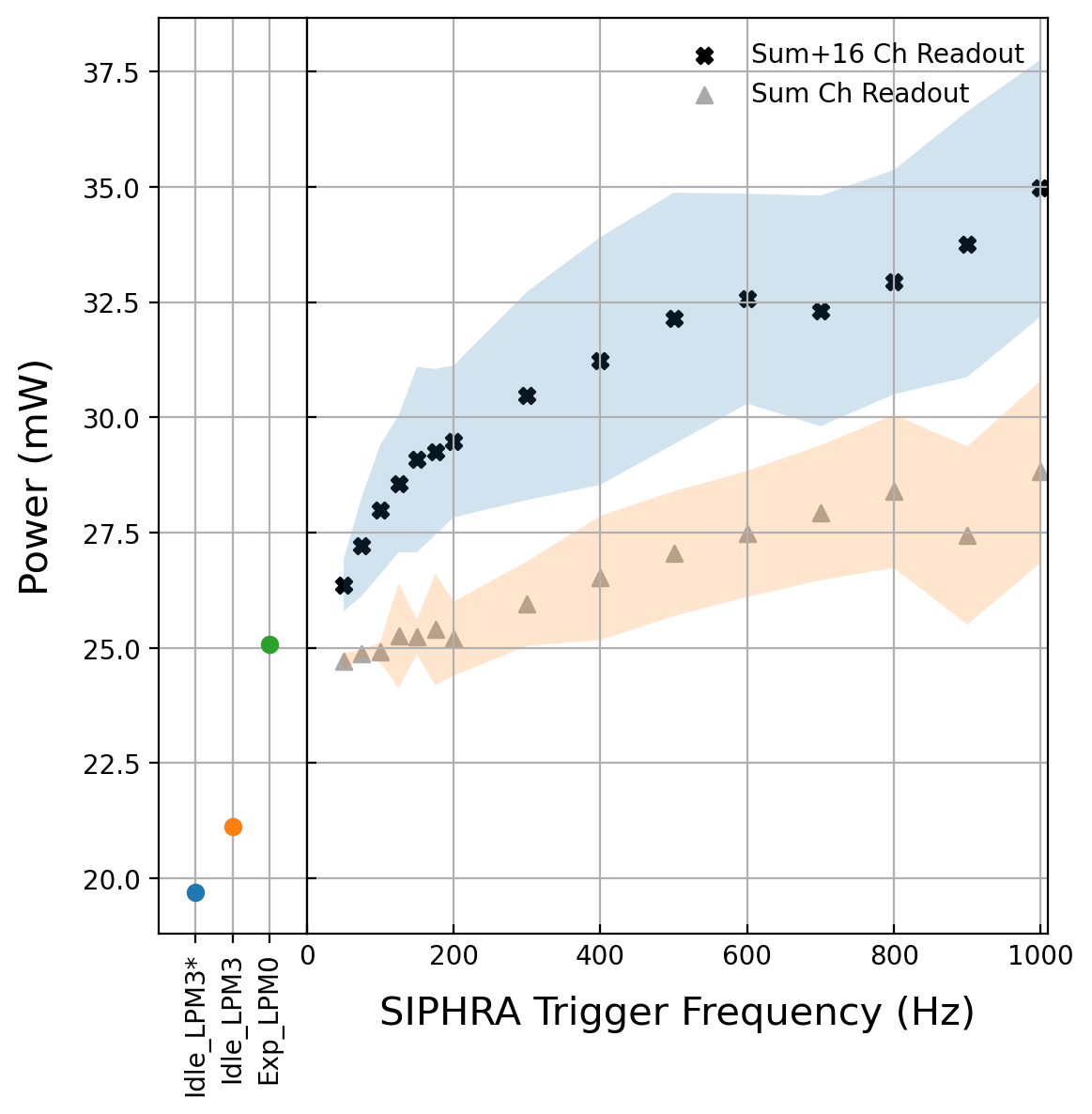
Figure 5 shows the power consumption from the 3.3 V line on the GMOD MB for the same range of trigger frequencies. The left hand panel shows the power consumption when GMOD is in Idle mode (IDLE_LPM3*) before the instrument configuration and just after programming, Idle mode (IDLE_LPM3) after configuration and finally Experiment mode (EXP_LPM0) before external triggering has begun. This highlights the use of LPM states as being advantageous, particularly on CubeSat missions where good power management is a must. As expected, summed and 16 channel readout together consume more power, increasing as a function of trigger frequency. In both cases the power consumption is less than the original estimate of 181.5 mW as defined in the DDF. It is interesting to note that the curves both have a set of breaks around trigger frequencies which have been seen in past testing to be the points when the MSP430 streaming buffers overflow and servicing from flash begins. The summed channel streaming buffer was seen to overflow 600-700 Hz – a break can be seen in both curves around this range. For the summed and 16 channel configuration, a break is also seen around 200 Hz – previously the 16 channel streaming buffer was seen to overflow 200 Hz. This is a somewhat unexpected, the reason why these notches appear is not yet known.
There are a number of caveats and limitations to these initial tests. Firstly, as a fixed duration of 30 seconds of TTE data is being selected across a number of trigger rates, there will be a dissimilar number of TTE samples for each trigger rate data point. Secondly, the use of a pulse generator which triggers SIPHRA readout at a fixed period is not fully representative of a realistic scenario and does not account for TTEs which have been successively triggered by gamma-ray interactions. During testing, it has been noticed that with the current firmware, the MSP430 has a maximum “dead time” of around 15 s which is caused by receive-side pointer setup; after receiving a TTE from the CPLD, it is likely that any subsequent TTE whose ASM is received within this 15 s window will not be registered and will be lost. Thirdly, as the SiPM array and scintillator were not used for this test, the current measurements used to calculate the power consumption exclude any contributions from the bias generation circuit. It is also difficult to isolate the current draw of the MSP430 from the rest of the circuits of the MB on the 3.3 V line, circuits whose power consumption may be a function of trigger rate and TTE throughput. Finally, at the time of testing, the CRC and coarse-timestamp were not included in the firmware, an exclusion which may have an influence on TTE throughput to the external flash memory.
VI Progress and Next Steps
The results presented here demonstrate the capability of the MSP430 to handle the transfer of data over the range required in orbit [11] and that the power consumption is within the expected range for a variety of modes and experiment configurations. While the MSP430 performs to the required specifications for EIRSAT-1, with the future aim of scaling the GMOD instrument up, it is likely that a bespoke system-on-a-chip would be required to handle the rates expected from a larger instrument. Development is currently on going with this firmware, which is not yet considered flight ready, but will be further improved and developed with rigorous testing of specific loading cases and a verification in the full functional[37] and mission testing[38] of the EIRSAT-1 Engineering Qualification Model and the Flight Model thereafter.
Acknowledgment
The EIRSAT-1 project is carried out with the support of ESA’s Education Office under the Fly Your Satellite! 2 programme. Students acknowledge support from the Irish Research Council, the School of Physics and School of Computer Science in UCD. We acknowledge all students who have contributed to EIRSAT-1. This study was supported Science Foundation Ireland (SFI) under grant number 17/CDA/4723 and by The European Space Agency’s Science Programme under contract 4000104771/11/NL/CBi. LH acknowledges support from SFI under grant 19/FFP/6777. DM, RD, and MD acknowledge support from the Irish Research Council (IRC) under grants GOIPG/2014/453, GOIPG/2019/2033 and GOIP/2018/2564 respectively. We acknowledge all students who have contributed to EIRSAT-1.
References
- [1] D.Murphy et al., “A Compact Instrument for Gamma–Ray Burst Detection on a CubeSat Platform II:Detailed Design and Laboratory Measurements,” Under Review, 2021.
- [2] G. Vedrenne, J.-L. Atteia, and L. Cominsky, Gamma-Ray Bursts: The Brightest Explosions in the Universe. Springer, 2009.
- [3] D. Murphy et al., “EIRSAT-: The Educational Irish Research Satellite,” Proceedings on the 2nd Symposium on Space Educational Activities, Apr 2018.
- [4] E. L. Shkolnik, “On the Verge of an Astronomy CubeSat Revolution,” Nature Astronomy, vol. Vol. 2, p. p.374–378, 2018.
- [5] CubeSat Design Specification, California Polytechnic State University, February 2014, Rev 13.
- [6] A. Ulyanov et al., “Performance of a Monolithic LaBr3:Ce Crystal Coupled to an Array of Silicon Photomultipliers,” Nuclear Instruments and Methods in Physics Research A, vol. 810, pp. 107–119, Feb 2016.
- [7] A. Ulyanov et al., “Localisation of Gamma-Ray Interaction Points in Thick Monolithic CeBr3 and LaBr3:Ce Scintillators,” Nuclear Instruments and Methods in Physics Research A, vol. 844, Feb 2017.
- [8] D. Murphy et al., “Balloon Flight Test of a CeBr3 Detector with Silicon Photomultiplier Readout,” Experimental Astronomy, 2021. [Online]. Available: https://doi.org/10.1007/s10686-021-09767-z
- [9] A. Ulyanov et al., “Radiation Damage Study of SensL J-Series Silicon Photomultipliers Using 101.4 MeV Protons,” Nuclear Instruments and Methods in Physics Research Section A, vol. 976, p. 164203, 2020.
- [10] J. Mangan et al., “The Environmental Test Campaign of GMOD, a Novel Gamma-Ray Detector,” Proceedings of the International Conference on Space Optics (ICSO), 2021. [Online]. Available: https://doi.org/10.1117/12.2599225
- [11] D. Murphy et al., “A Compact Instrument for Gamma–Ray Burst Detection on a CubeSat Platform I:Design Drivers and Expected Performance,” Accepted, 2021.
- [12] C. Meegan et al., “The Fermi Gamma-ray Burst Monitor,” The Astrophysical Journal, vol. 702, pp. 791–804, Sep. 2009.
- [13] C. Winkler et al., “The INTEGRAL Mission,” Astronomy and Astrophysics, vol. 411, pp. L1–L6, Nov. 2003.
- [14] J. Racusin et al., “BurstCube: A CubeSat for Gravitational Wave Counterparts,” arXiv e-prints, p. arXiv:1708.09292, Aug. 2017.
- [15] D. Zhang et al., “Energy Response of GECAM Gamma-Ray Detector Based on LaBr3:Ce and SiPM Array,” Nuclear Instruments and Methods in Physics Research Section A, vol. 921, pp. 8–13, 2019.
- [16] B. P. Abbott et al., “GW170817: Observation of Gravitational Waves from a Binary Neutron Star Inspiral,” Phys. Rev. Lett., vol. 119, p. 161101, Oct 2017.
- [17] A. Goldstein et al., “An Ordinary Short Gamma-Ray Burst with Extraordinary Implications: GBM Detection of GRB 170817A,” The Astrophysical Journal, vol. 848, no. 2, p. L14, Oct 2017.
- [18] D. Meier et al., “SIPHRA 16-Channel Silicon Photomultiplier Readout ASIC,” Proc. AMICSA & DSP 2016, 12-16 June 2016, Sweden, 06 2016.
- [19] A. Ulyanov et al., “Using the SIPHRA ASIC with an SiPM Array and Scintillators for Gamma Spectroscopy,” in 2017 IEEE Nuclear Science Symposium and Medical Imaging Conference, 2017, pp. 1–3.
- [20] M. Doyle et al., “Flight Software Development for the EIRSAT-1 Mission,” Proceedings of the 3rd Symposium on Space Educational Activities, 2020.
- [21] Zoglauer, A. and Andritschke, R. and Schopper, F., “MEGAlib The Medium Energy Gamma-ray Astronomy Library,” vol. 50, no. 7-8, pp. 629–632, Oct. 2006.
- [22] MSP430FR58xx, MSP430FR59xx, and MSP430FR6xx Family User’s Guide, Texas Instruments, October 2012, revised: April 2020.
- [23] MSP430FR599x, MSP430FR596x Mixed-Signal Microcontrollers Data Sheet, Texas Instruments, March 2016, revised: January 2021.
- [24] J. Schoolcraft, A. Klesh, and T. Werne, MarCO: Interplanetary Mission Development on a CubeSat Scale. Springer, 03 2017, pp. 221–231.
- [25] Maximizing Write Speed on the MSP430 FRAM, Texas Instruments, June 2011, revised Feb 2015.
- [26] S. M. Guertin, M. Amrbar, and S. Vartanian, “Radiation Test Results for Common CubeSat Microcontrollers and Microprocessors,” in 2015 IEEE Radiation Effects Data Workshop (REDW), 2015, pp. 1–9.
- [27] MSP430™ FRAM Quality and Reliability, Texas Instruments, March 2012, revised May 2014.
- [28] CubeSat Kit, 2021. [Online]. Available: http://www.cubesatkit.com/
- [29] Gaussteam, 2021. [Online]. Available: https://www.gaussteam.com
- [30] W. J. Ubbels et al., “Delfi-C3: a Student Nanosatellite as a Test-Bed for Thin Film Solar Cells and Wireless Onboard Communication,” in Proceedings of 2nd International Conference on Recent Advances in Space Technologies, 2005, pp. 167–172.
- [31] A. Klesh and et al., “Proceedings of the small satellite conference,” in Small Satellite Constellations: Strength in Numbers, 2013.
- [32] A. Aslan, E. Umit, M. Bas, M. Uludağ, I. Akyol, M. Aksulu, and E. Kalemci, “Development and in orbit testing of an x-ray detector within a 2u cubesat,” 09 2014.
- [33] Code Composer Studio - Texas Instruments, 2021. [Online]. Available: https://www.ti.com/tool/CCSTUDIO
- [34] Xilinx In-System Programming Using an Embedded Microcontroller (ISE Tools), Xilinx, May 2017, revised: May 2017.
- [35] The European Space Agency, ECSS‐M‐ST‐10C – Space project management: Project planning and implementation, 2009.
- [36] A. von Kienlin et al., “The Fourth Fermi-GBM Gamma-Ray Burst Catalog: A Decade of Data,” The Astrophysical Journal, vol. 893, no. 1, p. 46, Apr 2020.
- [37] S.Walsh et al., “Assembly Integration and Verification Activities for a 2U CubeSat EIRSAT-1,” Proceedings on the 3rd Symposium on Space Educational Activities, Apr 2020.
- [38] M. Doyle, R. Dunwoody, G. Finneran, D. Murphy, J. Reilly, J. Thompson, S. Walsh, and et al., “Mission Testing for Improved Reliability of CubeSats,” 2021. [Online]. Available: https://doi.org/10.1117/12.2600305