Observation of topological flat bands in the kagome semiconductor Nb3Cl8
Abstract
I Abstract
The destructive interference of wavefunctions in a kagome lattice can give rise to topological flat bands (TFBs) with a highly degenerate state of electrons. Recently, TFBs have been observed in several kagome metals, including Fe3Sn2, FeSn, CoSn, and YMn6Sn6. Nonetheless, kagome materials that are both exfoliable and semiconducting are lacking, which seriously hinders their device applications. Herein, we show that Nb3Cl8, which hosts a breathing kagome lattice, is gapped out because of the absence of inversion symmetry, while the TFBs survive because of the protection of the mirror reflection symmetry. By angle-resolved photoemission spectroscopy measurements and first-principles calculations, we directly observe the TFBs and a moderate band gap in Nb3Cl8. By mechanical exfoliation, we successfully obtain monolayer Nb3Cl8 which is stable under ambient conditions. In addition, our calculations show that monolayer Nb3Cl8 have a magnetic ground state, thus providing opportunities to study the interplay between geometry, topology, and magnetism.
Keywords: breathing kagome lattice, topological flat bands, semiconductor, ARPES, DFT calculations, mechanical exfoliation
The interplay between geometry, topology, and magnetism at the quantum level can give rise to rich physical properties, and the exploration of novel physics in nontrivial lattices is at the forefront of condensed matter physics LinZ2018 ; KangM2020NM ; KangM2020NC ; LiuZ2020 ; LiM2021 ; WeeksC2010 ; SunK2011 ; SlotMR2017 ; Kempkes2019 ; YinJ2020 ; LiuH2021 . A prototypical example is the kagome lattice that is composed of corner-sharing triangles [Fig. 1(a)]. Such a simple lattice has been intensively studied because of the emergence of topological band structures and frustration-driven spin-liquid states GuoHM2009 ; BalentsL2010 ; TangE2011 ; HanT2012 . Based on a simple -orbital tight-binding (TB) model with nearest-neighbour hopping, the electronic band structure of the kagome lattice can be described as a Dirac cone capped with a TFB [Fig. 1(b)]. The eigenfunctions at neighbouring corners have opposite phases, which results in a phase cancellation for hopping to neighbouring sites [black arrows in Fig. 1(a)]. Therefore, the electronic state is geometrically confined within a single hexagon; this real-space electronic localization leads to a TFB with quenched kinetic energy. The strong electron correlation effects in the highly degenerate flat band can give rise to various exotic properties, including high-temperature superconductivity ImadaM2000 ; JiangYX2021 , fractional quantum Hall effects TangE2011 , and Wigner crystal states JiangHC2017 ; JaworowskiB2018 .
Recently, TFBs and Dirac cones have been observed in several kagome metals by angle-resolved photoemission spectroscopy (ARPES), including Fe3Sn2 LinZ2018 ; YeL2018 , FeSn KangM2020NM , CoSn KangM2020NC ; LiuZ2020 , and YMn6Sn6 LiM2021 . However, most of the previously discovered kagome materials are metals without a band gap, which means that the “OFF” state cannot be achieved in devices. This drawback strongly limits their applications in logic and optoelectronic devices LiuY2016 ; LiuC2020 . Therefore, it is highly desirable to realize semiconducting kagome materials with a moderate band gap, in which the combination of semiconducting properties and TFBs might give rise to exotic physical phenomena, including gate-induced superconductivity YeJT2012 and triplet excitonic insulating state SethiG2021 . In addition, the realization of TFBs in semiconductors could enable the tuning of the TFBs by gating or chemical doping. On the other hand, an ideal kagome lattice is only one layer thick, and the non-negligible interlayer coupling in bulk materials will (partially) break the intrinsic properties of the kagome lattice. To date, experimental realization of layered and exfoliable kagome materials with TFBs is still challenging.
Here, we report a combined experimental and theoretical study on a breathing kagome material Nb3Cl8. Recently, the existence of TFBs in Nb3Cl8 has been predicted by a high-throughput screening LiuH2021 , but experimental investigations of its electronic structure are still lacking. Our ARPES and optical absorption spectroscopy measurements confirmed the existence of TFBs and a moderate band gap (1.12 eV). By mechanical exfoliation, we successfully obtained monolayer Nb3Cl8, a key step for device applications. In addition, Nb3Cl8 is expected to have a magnetic ground state, which implies the existence of exotic properties arising from the interplay between magnetism and band topology.
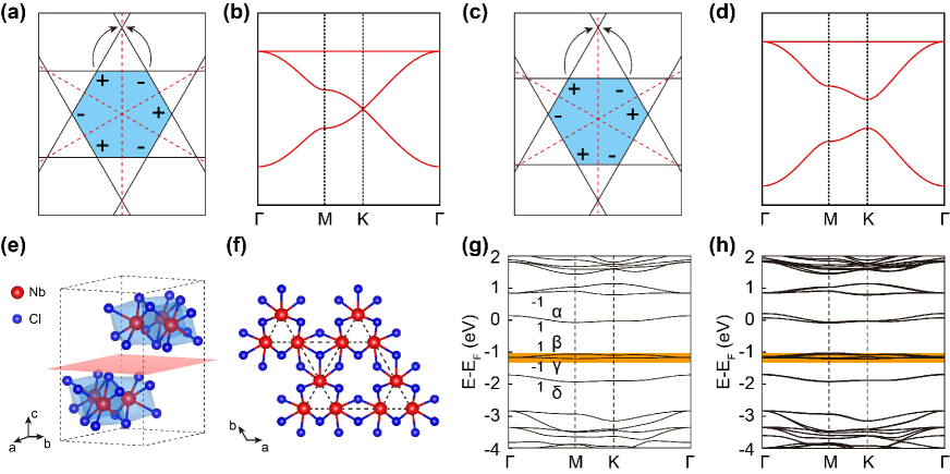
First, we briefly discuss the band structure of the breathing kagome lattice [Fig. 1(c)] based on a TB model. The degeneracy of the Dirac point in the conventional kagome lattice is protected by inversion symmetry. In the breathing kagome lattice, however, the absence of inversion symmetry will gap out the Dirac cone, leading to a semiconducting ground state, as shown in Fig. 1(d). On the other hand, destructive phase interference, the key reason for the emergence of TFBs, is protected by three equivalent mirror axes (red dashed lines in Fig. 1(a) and 1(c). These mirror symmetries survive in the breathing kagome lattice, and thus, the breathing kagome lattice still hosts TFBs. A detailed TB analysis is presented in the Supplementary Materials.
Next, we study a van der Waals material Nb3Cl8, which has a breathing kagome lattice in each layer MillerGJ1995 ; HaraguchiY2017 ; YoonJ2020 ; PascoCM2020 ; SheckeltonJP2017 . Bulk Nb3Cl8 crystallizes in a layered structure with a space group of P3̄m1 [Fig. 1(e)]. Within each layer, the Nb atoms form a breathing kagome lattice, as shown in Fig. 1(f). The calculated band structure of monolayer Nb3Cl8 is displayed in Fig. 1(g). One can directly see a flat band at approximately 1.1 eV below the Fermi level, which has the narrowest bandwidth, as highlighted by the orange region. In addition, our orbital and symmetry analysis has confirmed the phase destructive interfering behavior of this band, which is the key character of kagome TFBs (see Supporting Information for details). The Dirac cones are gapped out, resulting in multiple gaps. Notably, the band crosses the Fermi level, indicating a metallic ground state. However, we will show later that the ground state should be semiconducting because DFT calculations underestimate the gap, as confirmed by our ARPES and optical absorption spectroscopy measurements. Because of the weak interlayer van der Waals interaction, the band structure of bulk Nb3Cl8 is analogous to that of monolayer Nb3Cl8, as shown in Fig. 1(h). As a result, the TFBs survive in bulk Nb3Cl8, which is favourable for ARPES measurements.
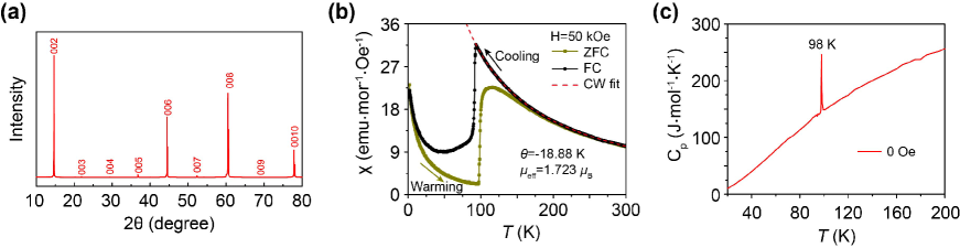
High-quality Nb3Cl8 single crystals were synthesized by the self-flux method (see the Methods section). Figure 2(a) shows an XRD spectrum measured along the (00l) direction, and only the 00l peaks were observed. The sharp peaks indicate the high quality of the crystals. The temperature-dependent magnetic susceptibility of Nb3Cl8 is displayed in Fig. 2(b). As the temperature decreases, the magnetic susceptibility of Nb3Cl8 drops abruptly at 100 K with a prominent hysteresis. Above 100 K, the temperature dependence of the magnetic susceptibility can be well fitted by the Curie-Weiss function, as indicated by the red dashed line in Fig. 2(b), and the fitted value is -18.88 K. The negative value indicates an antiferromagnetic ground state. These results agree well with previous works HaraguchiY2017 . In addition, the heat capacity shows a sharp -shaped peak at approximately 98 K [Fig. 2(c)], in line with the transition temperature determined from the magnetic susceptibility measurements. This phase transition were interpreted as a slight change in layer stacking, which does not affect the structure within each layer HaraguchiY2017 . Therefore, the topological properties of Nb3Cl8 are not affected by the phase transition either.
We then performed ARPES measurements to confirm the TFBs in Nb3Cl8. Because of the semiconducting nature of Nb3Cl8, there is no detectable photoemission signal at the Fermi level. With increasing binding energies, we observe strong spectral weight near the point of the first Brillouin zone (BZ) from 0.8 eV, as shown in Fig. 3(a). The spectral weight in the second BZ is much weaker because of the photoemission matrix element effect. The constant energy contour at 2.6 eV shows clear hexagonal symmetry [Fig. 3(b)], in agreement with the crystal structure of Nb3Cl8. The band structures along the - and - directions are displayed in Fig. 3(c)-3(i). A careful comparison with the calculation results shows that the chemical potential has a 0.8 eV shift towards higher binding energies. After readjusting the chemical potential, the calculated band structures agree well with our ARPES results except for a slight discrepancy at the Fermi level, as indicated by the red dashed lines. The discrepancy at the Fermi level will be discussed later. Within 3.5 eV of the Fermi level, we observed four prominent bands: , , , and . Notably, the TFB, i.e., the band can be observed in the whole BZ and has negligible dispersion, as shown in Fig. 3(e),(f),(j). The band, which is very close to the band, has a stronger spectral weight with low photon energies [Fig. 3(i)]. In contrast with the flat band, the band disperses with momentum, as shown in Fig. 3(k). Figure 3(l) shows the fitted dispersions of the four bands, which agree well with our calculation results.
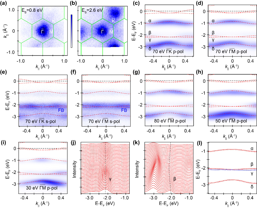
During ARPES measurements, we find that the spectral weight of each band varies with the polarization of the incident light: the , , and bands are more sensitive to -polarized light, while the band is more sensitive to -polarized light, despite the intensity variation with photon energy. To understand this phenomenon, we focus on the bands along - because - is a mirror axis and each band along this direction has definite odd or even parity when spin-orbit coupling is neglected. The calculation results are indicated by “+” (even) and “-” (odd) in Fig. 1(g). We find that the , , and bands have even parity, which can only be observed by -polarized light. The band, i.e., the flat band has odd parity and can only be detected by -polarized light. These analyses agree well with our ARPES results, which further confirms the existence of TFBs in Nb3Cl8. Neglecting the variation in relative intensity, we find that all bands have negligible dispersion with photon energy (or ), in agreement with the two-dimensional nature of Nb3Cl8.
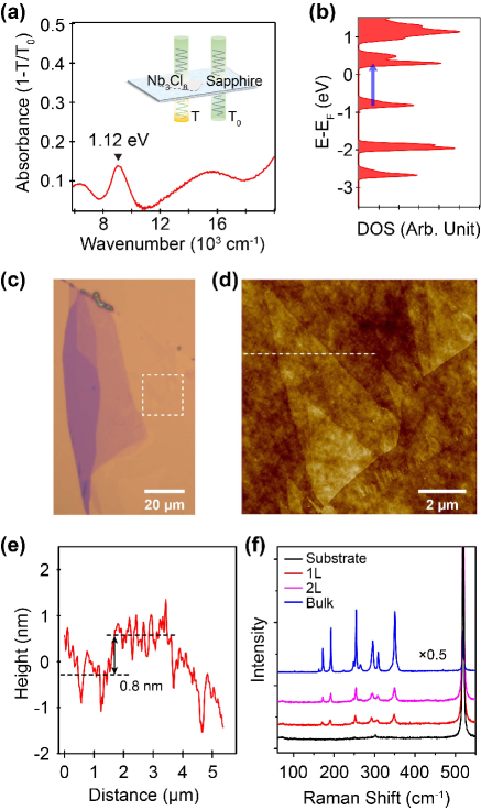
Next, we discuss the discrepancy near the Fermi level between the experimental and calculation results: the calculation results show the existence of bands after adjusting the chemical potential, while we did not observe any bands in our ARPES measurements. A possible reason for this discrepancy is the underestimation of the band gap in DFT calculations PerdewJP2017 . Based on our ARPES results, the valence band maximum is located at 0.9 eV below the Fermi level, which indicates that the actual band gap is larger than 0.9 eV. To determine the band gap of Nb3Cl8, we performed optical absorption spectroscopy measurements. Figure 4(a) shows a typical absorption spectrum of Nb3Cl8, and several absorption peaks are observed from the ultraviolet to near-infrared regions. There is one prominent peak at 1.12 eV, which can be assigned to the transition from valence to conduction bands, as indicated by the blue arrow in Fig. 4(b). Therefore, the optical band gap is 1.12 eV, which is approximately 0.23 eV larger than the calculation results. It should be noted that there is a broader peak centred at 6250 cm-1 (0.775 eV). This feature is within the band gap and might originate from defects or edge states RoxloCB1986 ; ChenJ2021 . Since the valence band maximum is located at 0.9 eV, the conduction band bottom is expected to be located at 0.22 eV above the Fermi level, which is not accessible in our ARPES measurements.
Thus far, we have demonstrated that Nb3Cl8 hosts TFBs because of the breathing kagome lattice. Strictly speaking, however, a kagome lattice refers to monolayer materials; the non-negligible interlayer coupling in bulk materials could be detrimental to the intrinsic properties of the kagome lattice. Therefore, it is highly desirable to obtain monolayer kagome materials for their applications in quantum devices. Because of the weak van der Waals interaction in bulk Nb3Cl8, ultrathin flakes can be easily obtained by mechanical exfoliation YoonJ2020 . Figure 4(c) shows a typical optical microscope image of an ultrathin Nb3Cl8 flake, and Figure 4(d) shows an atomic force microscopy (AFM) image in the white box of Fig. 4(c). The height of the thinnest flake is approximately 0.8 nm with respect to the substrate [Fig. 4(e)], which is comparable to the lattice constant of bulk Nb3Cl8 in the perpendicular direction (0.61 nm). The quality of ultrathin Nb3Cl8 was also confirmed by Raman spectroscopy measurements, as shown in Fig. 4(f). Most of the Raman peaks of the bulk Nb3Cl8 survive in the monolayer limit with negligible shift. It should be noted that our AFM and Raman spectroscopy measurements were performed under ambient conditions, and the strong intensity of Raman peaks indicates the high stability of monolayer Nb3Cl8 in air. Stability in air is an essential prerequisite for potential device applications.
To summarize, we provide compelling evidence for the existence of TFBs in Nb3Cl8 which has a breathing kagome lattice. The semiconducting nature of Nb3Cl8 provides opportunities to fabricate optoelectronic and logic devices. Few- and monolayer Nb3Cl8 can be easily obtained by mechanical exfoliation and are quite stable under ambient conditions, which is an essential prerequisite for their device applications. In addition, our calculations show that the ground state of monolayer Nb3Cl8 is ferromagnetic and the TFBs will spin split because of the magnetic exchange interaction (see Supplementary Materials). In contrast with conventional and nonmagnetic kagome lattices, the breaking of symmetries in breathing kagome lattices, including inversion and time reversal, can give rise to multiple topological states, such as higher-order topological insulators/semimetals BolensA2019 ; WakaoH2020 ; EzawaM2018 , Chern insulators RenY2021 , and chiral charge densities JiangYX2021 .
II Methods
Single crystals of Nb3Cl8 were grown using PbCl2 as a flux. High-purity Nb (Alfa Aesar 99.99%) and NbCl5 (Alfa Aesar 99.9%) were mixed at a molar ratio of 7:8 and placed in an alumina crucible. The crucible was sealed in a quartz tube under vacuum, heated at 750 ∘C for 150 hours, and cooled to room temperature naturally. The excess PbCl2 flux was removed by sonicating in hot water. ARPES measurements were performed at Beamline BL-1 of the Hiroshima Synchrotron Radiation Center IwasawaH2017 . Clean surfaces required for the ARPES measurements were obtained by cleaving the samples in situ in an ultrahigh vacuum chamber. Both the cleavage and the measurements were performed at room temperature to avoid charging effects. Nb3Cl8 thin flakes can be exfoliated on various substrates, including SiO2/Si, Au/SiO2/Si, and sapphire, using blue Nitto tapes. Freshly cleaved surfaces were attached to the precleaned substrates, followed by carefully peeling off the tape. Thin flakes that contain few- to monolayer Nb3Cl8 remained on the substrates. The thicknesses and morphologies of Nb3Cl8 flakes were examined by AFM (Oxford, Asylum Research Cypher S) in tapping mode. Raman spectra were collected using a confocal Raman system (Horiba LanRam HR Evolution) with 532-nm laser excitation. Optical absorption measurements were carried out using a commercial spectrometer (MStarter ABS, Metatest Corporation).
First-principles calculations based on density functional theory were performed with the Vienna ab initio simulation package KresseG1993 ; KresseG1996prb . The projector-augmented wave pseudopotential BlochlPE1994 and Perdew-Burke-Ernzerhof exchange-correlation functional PerdewJP1996 were used. The energy cutoff of the plane-wave basis was set at 350 eV. For monolayer Nb3Cl8, the vacuum space was set to be larger than 15 Å. The first BZ was sampled according to the -centred scheme. For monolayer (bulk) Nb3Cl8, we used a mesh of 661 (666) for structural optimization and 12121 (999) for the self-consistent calculations. The positions of the atoms were optimized until the convergence of the force on each atom was less than 0.01 eV/Å. The convergence condition of the electronic self-consistent loop was 10-5 eV.
III Associated Content
Supporting Information
Generalizing the destructive phase interference to breathing kagome lattice; Inversion symmetry breaking induced gap opening in the kagome lattice; Determining the magnetic ground state of monolayer Nb3Cl8; Topological properties of the flat bands in Nb3Cl8; Orbital and symmetry analysis of the flat band.
IV Acknowledgement
This work was supported by the Ministry of Science and Technology of China (Grant No. 2018YFE0202700), the National Natural Science Foundation of China (Grants No. 11974391, No. 11825405, No. 1192780039, and No. U2032204), the Beijing Natural Science Foundation (Grant No. Z180007), the International Partnership Program of Chinese Academy of Sciences (Grant No. 112111KYSB20200012), and the Strategic Priority Research Program of Chinese Academy of Sciences (Grants No. XDB33030100). ARPES measurements were performed under the Proposal No. 21AU002. We thank the N-BARD, Hiroshima University for supplying liquid He.
V Author Contributions
B.F. conceived the research. C.W., X.H., Y.H., and Y.S. synthesized the crystals; Z.S., S.K., D.G., S.Y., and B.F. performed the ARPES measurements; H.Z. and S.M. performed theoretical calculations and analysis; all authors contributed to the discussion of the data and writing of the manuscript. Z.S, H.Z., C.W., and S.K. contributed equally to this work.
VI Notes
The authors declare no competing financial interests.
VII References
References
- (1) Lin, Z.; Choi, J.-H.; Zhang, Q.; Qin, W.; Yi, S.; Wang, P.; et al. Flatbands and emergent ferromagnetic ordering in Fe3Sn2 kagome lattices. Phys. Rev. Lett. 2018, 121, 096401.
- (2) Kang, M.; Ye, L.; Fang, S.; You, J.-S.; Levitan, A.; Han, M.; et al. Dirac fermions and flat bands in the ideal kagome metal FeSn. Nat. Mater. 2020, 19, 163-169.
- (3) Kang, M.; Fang, S.; Ye, L.; Po, H. C.; Denlinger, J.; Jozwiak, C.; Bostwick, A.; Rotenberg, E.; Kaxiras, E.; Checkelsky, J. G.; Comin, R. Topological flat bands in frustrated kagome lattice CoSn. Nat. Commun. 2020, 11, 4004.
- (4) Liu, Z.; Li, M.; Wang, Q.; Wang, G.; Wen, C.; Jiang, K.; Lu, X.; Yan, S.; Huang, Y.; Shen, D.; Yin, J.-X.; Wang, Z.; Yin, Z.; Lei, H.; and Wang, S. Orbital-selective Dirac fermions and extremely flat bands in frustrated kagome-lattice metal CoSn. Nat. Commun. 2020, 11, 4002.
- (5) Li, M.; Wang, Q.; Wang, G.; Yuan, Z.; Song, W.; Lou, R.; Liu, Z.; Huang, Y.; Liu, Z.; Lei, H.; Yin, Z.; Wang, S. Dirac cone, flat band and saddle point in kagome magnet YMn6Sn6. Nat. Commun. 2021, 12, 3129.
- (6) Weeks C.; Franz, M. Topological insulators on the Lieb and perovskite lattices. Phys. Rev. B 2010, 82, 085310.
- (7) Sun, K.; Gu, Z.; Katsura, H.; Sarma, S. D. Nearly flatbands with nontrivial topology. Phys. Rev. Lett. 2011, 106, 236803.
- (8) Slot, M. R.; Gardenier, T. S.; Jacobse, P. H.; van Miert, G. C. P.; Kempkes, S. N.; Zevenhuizen, S. J. M.; Smith, C. M.; Vanmaekelbergh, D.; Swart, I. Experimental realization and characterization of an electronic Lieb lattice. Nat. Phys. 2017, 13, 672-676.
- (9) Kempkes, S. N.; Slot, M. R.; van den Broeke, J. J.; Capiod, P.; Benalcazar, W. A.; Vanmaekelbergh, D.; Bercioux, D.; Swart, I.; Smith, C. M. Robust zero-energy modes in an electronic higher-order topological insulator. Nat. Mater. 2019, 18, 1292-1297.
- (10) Yin, J.; Ma, W.; Cochran, T. A.; Xu, X.; Zhang, S. S.; Tien, H. J.; et al. Quantum-limit Chern topological magnetism in TbMn6Sn6. Nature 2020, 583, 533-536.
- (11) Liu, H.; Meng, S.; Liu, F. Screening two-dimensional materials with topological flat bands. Phys. Rev. Mater. 2021, 5, 084203.
- (12) Guo H.-M.; Franz, M. Topological insulator on the kagome lattice. Phys. Rev. B 2009, 80, 113102.
- (13) Balents, L. Spin liquids in frustrated magnets. Nature 2010, 464, 199-208.
- (14) Tang, E.; Mei, J.-W.; Wen, X.-G. High-temperature fractional quantum Hall states. Phys. Rev. Lett. 2011, 106, 236802.
- (15) Han, T.-H.; Helton, J. S.; Chu, S.; Nocera, D. G.; Rodriguez-Rivera, J. A.; Broholm, C.; Lee, Y. S. Fractionalized excitations in the spin-liquid state of a kagome lattice antiferromagnet. Nature 2012, 492, 406-410.
- (16) Imada, M.; Kohno, M. Superconductivity from flat dispersion designed in doped Mott insulators. Phys. Rev. lett. 2000, 84, 143.
- (17) Jiang, Y.-X.; Yin, J.-X.; Denner, M. M.; Shumiya, N.; Ortiz, B. R.; Xu, G.; et al. Unconventional chiral charge order in kagome superconductor KV3Sb5. Nat. Mater. 2021, 20, 1353-1357.
- (18) Jiang, H.-C.; Devereaux, T.; Kivelson, S. A. Holon Wigner crystal in a lightly doped kagome quantum spin liquid. Phys. Rev. Lett. 2017, 119, 067002.
- (19) Jaworowski, B.; Güçlü, A. D. G.; Kaczmarkiewicz, P.; Kupczyński, M.; Potasz, P.; Wójs, A. Wigner crystallization in topological flat bands. New J. Phys. 2018, 20, 063023.
- (20) Lin, Y.; Kang, M.; Liu, J.; von Cube, F.; Wicker, C. R.; Suzuki, T.; Jozwiak, C.; Bostwick, A.; Rotenberg, E.; Bell, D. C.; Fu, L.; Comin, R.; Checkelsky, J. G. Massive Dirac fermions in a ferromagnetic kagome metal. Nature 2018, 555, 638-642.
- (21) Liu, Y.; Weiss, N. O.; Duan, X.; Cheng, H.-C.; Huang, Y.; Duan, X. Van der Waals heterostructures and devices. Nat. Rev. Mater. 2016, 1, 16042.
- (22) Liu, C.; Chen, H.; Wang, S.; Liu, Q.; Jiang, Y.-G.; Zhang, D. W.; Liu, M.; Zhou, P. Two-dimensional materials for next-generation computing technologies. Nat. Nanotechnol. 2020, 15, 545-557.
- (23) Ye, J. T.; Zhang, Y. J.; Akashi, R.; Bahramy, M. S.; Arita, R.; Iwasa, Y. Superconducting dome in a gate-tuned band insulator. Science 2012, 338, 1193-1196.
- (24) Sethi, G.; Zhou, Y.; Zhu, L.; Yang, L.; Liu, F. Flat-band-enabled triplet excitonic insulator in a diatomic kagome lattice. Phys. Rev. Lett. 2021, 126, 196403.
- (25) Miller, G. J. Solid state chemistry of Nb3C18: Nb3TeC17, mixed crystal formation, and intercalation. J. Alloys Compd. 1995, 217, 5-12.
- (26) Haraguchi, Y.; Michioka, C.; Ishikawa, M.; Nakano, Y.; Yamochi, H.; Ueda, H.; Yoshimura, K. Magnetic-nonmagnetic phase transition with interlayer charge disproportionation of Nb3 trimers in the cluster compound Nb3Cl8. Inorg. Chem. 2017, 56, 3483-3488.
- (27) Yoon, J.; Lesne, E.; Sklarek, K.; Sheckelton, J.; Pasco, C.; Parkin, S. S. P; McQueen, T. M.; Ali, M. N. Anomalous thickness-dependent electrical conductivity in van der Waals layered transition metal halide, Nb3Cl8. J. Phys.: Condens. Matter, 2020, 32, 304004.
- (28) Pasco, C. M.; El Baggari, I.; Bianco, E.; Kourkoutis, L. F.; McQueen, T. M. Tunable magnetic transition to a singlet ground state in a 2D van der Waals layered trimerized kagome magnet. ACS Nano, 2019, 13, 9457-9463.
- (29) Sheckelton, J. P.; Plumb, K. W.; Trump, B. A.; Broholmbcd, C. L.; McQueen, T. M. Rearrangement of van der Waals stacking and formation of a singlet state at T=90 K in a cluster magnet. Inorg. Chem. Front. 2017, 4, 481-490.
- (30) Perdew, J. P.; Yang, W.; Burke, K.; Yang, Z.; Gross, E. K. U.; Scheffler, M.; Scuseria, G. E.; Henderson, T. M.; Zhang, I. Y.; Ruzsinszky, A.; Peng, H.; Sun, J.; Trushin, E.; Görling, A. Understanding band gaps of solids in generalized Kohn-Sham theory. Proc. Natl. Acad. Sci. U. S. A. 2017, 114, 2801-2806.
- (31) Roxlo, C. B.; Daage, M.; Rupper, A. F.; Chianelli, R. R. Optical absorption and catalytic activity of molybdenum sulfide edge surfaces. J. Catal. 1986, 100, 176-184.
- (32) Chen, J.; Wang, J.; Yu, Q.; Wang, T.; Zhang, Y.; Chen, C.; Li, C.; Wang, Z.; Zhu, S.; Ding, X.; Wang, L.; Wu, J.; Zhang, K.; Zhou, P.; Jiang, Z. Sub-band gap absorption and optical nonlinear response of MnPSe3 nanosheets for pulse generation in the L-band. ACS Appl. Mater. Interfaces 2021, 13, 13524-13533.
- (33) Bolens, A.; Nagaosa, N. Topological states on the breathing kagome lattice. Phys. Rev. B 2019, 99, 165141.
- (34) Wakao, H.; Yoshida, T.; Araki, H.; Mizoguchi, T.; Hatsugai, Y. Higher-order topological phases in a spring-mass model on a breathing kagome lattice. Phys. Rev. B 2020, 101, 094107.
- (35) Ezawa, M. Higher-order topological insulators and semimetals on the breathing kagome and pyrochlore lattices. Phys. Rev. Lett. 2018, 120, 026801.
- (36) Ren, Y.; Jiang, H.-C.; Qiao, Z.; Sheng, D. Orbital chern insulator and quantum phase diagram of a kagome electron system with half-filled flat bands. Phys. Rev. Lett. 2021, 126, 117602.
- (37) Iwasawa, H.; Shimada, K.; Schwier, E. F.; Zheng, M.; Kojima, Y.; Hayashi, H.; Jiang, J.; Higashiguchi, M.; Aiura, Y.; Namatame, H.; Taniguchi, M. Rotatable high-resolution ARPES system for tunable linear-polarization geometry. J. Synchrotron Radiat. 2017, 24, 836-841.
- (38) Kresse, G.; Hafner, J. Ab initio molecular dynamics for liquid metals. Phys. Rev. B 1993, 47, 558(R).
- (39) Kresse, G.; Furthmüller, J. Efficient iterative schemes for ab initio total-energy calculations using a plane-wave basis set. Phys. Rev. B 1996, 54, 11169-11186.
- (40) Blöchl, P. E. Projector augmented-wave method. Phys. Rev. B 1994, 50, 17953-17979.
- (41) Perdew, J. P.; Burke, K.; Ernzerhof, M. Generalized gradient approximation made simple. Phys. Rev. Lett. 1996, 77, 3865.