50 Ohm Transmission Lines with Extreme Wavelength Compression Based on Superconducting Nanowires on High-Permittivity Substrates
Abstract
We demonstrate impedance-matched low-loss transmission lines with a signal wavelength more than 150 times smaller than the free space wavelength using superconducting nanowires on high permittivity substrates. A niobium nitride thin film is patterned in a coplanar waveguide (CPW) transmission line geometry on a bilayer substrate consisting of 100 nm of epitaxial strontium titanate on high-resitivity silicon. The use of strontium titanate on silicon enables wafer-scale fabrication and maximizes process compatibility. It also makes it possible to realize a characteristic impedance across a wide range of CPW widths, from the nanoscale to the macroscale. We fabricated and characterized an approximately CPW device with two half-wave stub resonators. Comparing the measured transmission coefficient to numerical simulations, we determine that the strontium titanate film has a dielectric constant of and a loss tangent of not more than 0.009. To facilitate the design of distributed microwave devices based on this type of material system, we describe an analytical model of the CPW properties that gives good agreement with both measurements and simulations.
Cryogenic microwave circuitry has garnered increased interest in recent years, driven in part by the field of quantum computing based on superconducting circuits.Schoelkopf and Girvin (2008); Kjaergaard et al. (2020); Wendin (2017) It is also important for the development of large-format arrays of cryogenic particle detectorsWollman et al. (2019) and high-speed classical computing using superconducting circuits.Tolpygo (2016) The size of distributed microwave components – such as filters, resonators, couplers, circulators, and travelling wave parametric amplifiers – is limited by the signal wavelength, which is cm at 5 GHz in standard material systems. This large size makes on-chip integration difficult and is one of the major bottlenecks in scaling up cryogenic microwave systems.Gambetta, Chow, and Steffen (2017); Hornibrook et al. (2015); Brecht et al. (2016)
For low-loss transmission lines, the characteristic impedance is and the phase velocity is , where is the inductance per unit length and is the capacitance per unit length. The ratio of the signal wavelength on the transmission line to the free space wavelength is the same as the ratio of the phase velocity on the transmission line to the speed of light in free space. Standard transmission lines, such as an RG-58 coaxial cable or a microstrip on FR4 circuit board, have a signal wavelength that is approximately two thirds of the free space wavelength. The signal wavelength can be reduced while maintaining a matched impedance by proportionally increasing both and . Previous work has developed slow-wave transmission lines using conventional materials and increasing and by manipulating the transmission line geometry.Seki and Hasegawa (1981); Chang and Chang (2012); Rosa et al. (2018) This approach has been successful in reducing the signal velocity and wavelength by up to an order of magnitude but not further.
Superconducting nanowires made from low carrier density materials can have a kinetic inductance that is two or more orders of magnitude larger than their magnetic inductance.Annunziata et al. (2010); Hazard et al. (2019); Grünhaupt et al. (2019) One such material is niobium nitride (NbN), which has demonstrated inductances per unit length pH/m in a 100 nm wide, ultra-thin nanowire.Annunziata et al. (2010); Santavicca et al. (2016) This compares to a magnetic inductance of pH/m. The large kinetic inductance naturally leads to a large characteristic impedance, , when patterned in a transmission line geometry.Santavicca et al. (2016); Colangelo et al. (2021) Such large impedances can be useful for decoupling from the electromagnetic environment but create challenges for coupling to standard microwave circuitry, which is commonly designed around a impedance. Incorporating the nanowire in a high permittivity dielectric medium brings down the characteristic impedance and further shrinks the signal wavelength. High permittivity oxides such as hafnium dioxide (dielectric constant ) and titantium dioxide () offer significant enhancement over silicon dioxide ()Robertson (2004) but do not have a large enough permittivity to offset the extremely large kinetic inductance of a NbN nanowire in order to achieve a characteristic impedance.
Advances in materials science have allowed the synthesis of ceramic materials belonging to the class of perovskites with extremely high relative permittivities. One such material, strontium titanate (SrTiO3, abbreviated as STO), is a quantum paraelectric with an indirect bandgap of eV.Pai et al. (2018) It has been shown to have a relative permittivity exceeding in single crystal form at K, a value that decreases upon the application of an external electric field.Sakudo and Unoki (1971) This permittivity is sufficiently large to achieve a characteristic impedance with a NbN nanowire. However, as the wire width increases, the kinetic inductance decreases, and the extreme permittivity of STO results in macroscale transmission lines with characteristic impedances well below .Davidovikj et al. (2017)
In order to achieve a characteristic impedance at both nanoscale and macroscale dimensions, we have utilized a thin layer of STO grown epitaxially on a bulk silicon (Si) wafer.Li et al. (2003); Warusawithana et al. (2009) At nanoscale dimensions, the STO dominates the effective permittivity, but as the transmission line width increases, the contribution of the STO to the effective permittivity decreases. The use of bulk Si also ensures the ability to fabricate on large-scale substrates, as single-crystal STO is generally not available in substrate sizes larger than two inches.Guguschev et al. (2015) Further, Si is a widely used substrate material, so its use increases process compatibility with other types of cryogenic and superconducting circuitry.
Previous work described CPW resonators made from the high-temperature superconductor YBa2Cu3O7-x on substrates consisting of an STO film on bulk LaAlO3.Findikoglu et al. (1995); M.Adam, D.Fuchs, and R.Schneider (2002) This work focused on utilizing the electric field-dependent polarizability of the STO to realize resonator tunability and the devices exhibited only modest compression of the signal wavelength by a factor of 2-3 compared to the free space value.
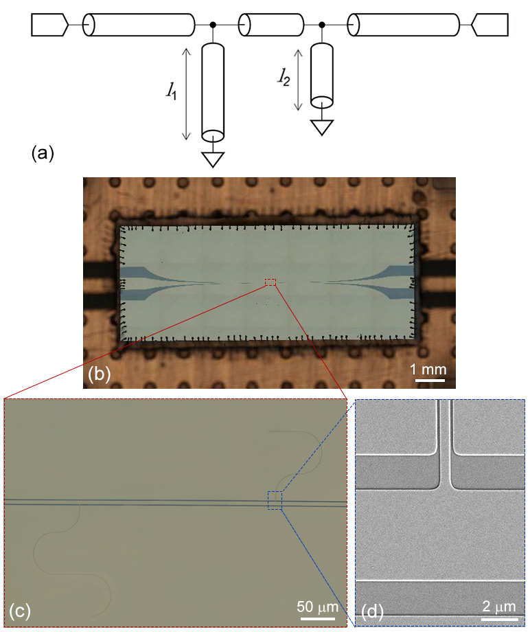
To demonstrate the potential for extreme wavelength compression using our material system, we fabricated the coplanar waveguide (CPW) double resonator device shown in figure 1. The device maintains a characteristic impedance of approximately , with a CPW that transitions from a center conductor width of m and a gap width between the center conductor and the coplanar grounds of m at the edges of the chip – large enough to facilitate wirebonding – to a center conductor width of m and a gap width of m in the center of the chip. The transition maintains a constant fractional change in the center conductor width per unit length. In the center section, two half-wave stub resonators connect between the center conductor of the main CPW and ground. The resonators are in a CPW geometry with a center conductor width of nm and a gap width of nm. The length of the longer resonator is m and the length of the shorter resonator is m. An equivalent circuit model is shown in figure 1a.
The substrate consists of 100 nm of epitaxial (001) STO grown via molecular beam epitaxy (MBE) on a 370 m thick high-resistivity (001) Si ( kcm). The initiation of the heteroepitaxial growth of STO on Si is key to obtaining a crystalline STO filmWarusawithana et al. (2009) and involves a controlled sequence of steps that kinetically suppresses the formation of an amorphous oxide layer on SiWarusawithana et al. (2009); Li et al. (2003) and reduces the tendency for the STO film to form islands.Kourkoutis et al. (2008) Once a thin crystalline STO template was formed with in-plane epitaxial relationship STO [100] parallel to Si [110], the growth conditions were maintained at C substrate temperature and Torr oxygen background pressure to obtain a 260 molecular-layer thick (100 nm) STO film. Throughout the growth, reflection high energy electron diffraction (RHEED) patterns showed good crystalline quality of the film. See the Supplementary Material for additional growth details. Crystal quality was also evaluated using post-growth x-ray diffraction measurements: rocking curve measurements in of the out-of-plane STO 002 reflection showed a full-width at half-maximum of . To minimize oxygen vacancies which could lead to increased dielectric losses, the film was cooled down to below ∘C under an oxygen background pressure of Torr before removing the sample from the MBE chamber.
A nm thick NbN filmMedeiros et al. (2019) was deposited on the STO-Si substrate via reactive magnetron sputtering of niobium in the presence of nitrogen gas on the room temperature substrate. The device was patterned using 125 kV electron beam lithography with ZEP530A (Zeon corp.) positive tone resist. The patterns were developed in o-Xylene at ∘C and were transferred into NbN with reactive ion etching in a CF4 plasma. After etching, the resist residues were removed with N-Methyl-2-pyrrolidone. The measured critical temperature of the device was K and the switching current measured between one end of the CPW center conductor and ground – i.e. measuring the two resonators in parallel – was 813 A at a temperature of 1.5 K.
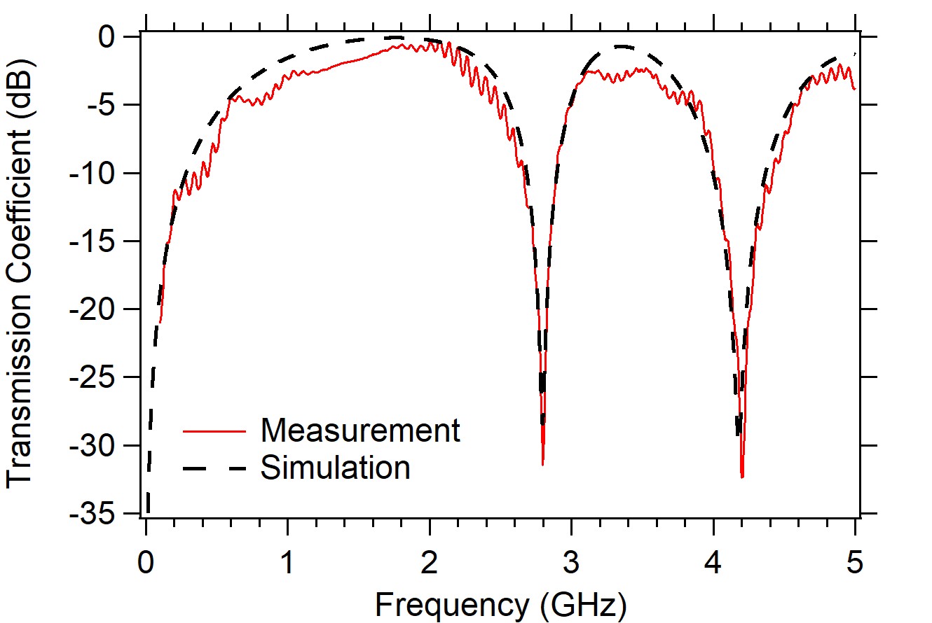
The transmission coefficient of this device measured at a bath temperature K is shown in figure 2. A schematic of the experimental setup can be seen in the Supplementary Material. The signal power at the device is less than dBm, ensuring that we do not excite non-linear effects. The data are normalized by measuring a sample with the same CPW geometry but no resonators. The fundamental half-wave resonances occur at 2.80 GHz and 4.20 GHz, corresponding to a signal wavelength on the resonators that is 178 times smaller than the free space wavelength.
Also shown in figure 2 is a simulation of the device using the AXIEM solver in AWR Microwave Office with an appropriately small mesh size. The dielectric anisotropy of STO is ignored in the simulation, and the superconducting NbN is modeled as a complex sheet impedance with a real part of zero and the imaginary part set to with the simulation frequency and the sheet kinetic inductance.Santavicca et al. (2016) can be determined from the normal-state sheet resistance using
| (1) |
where is Planck’s constant, is the superconducting energy gap, and is Boltzmann’s constant.Annunziata et al. (2010) In the limit that the temperature is much smaller than the superconducting critical temperature , and the previous equation simplifies to . In order to measure without possible error due to substrate conductivity, a NbN film was deposited on a thermally-oxidized Si chip at the same time as the deposition on the STO-Si chip. This sample has per square at K, corresponding to pH per square in the low temperature () limit, which is the value used in the simulation.
The values of the STO dielectric constant and loss tangent are adjusted in the simulation to achieve the best agreement with the data. This leads to a dielectric constant of . The corresponding characteristic impedance of the resonator CPW is 66 , close to the target value of . The CPW gap size could be reduced to bring the impedance closer to the target value. While the STO permittivity is lower than values reported for bulk single crystals, it is comparable to previously reported values for thin-film STO,Li et al. (1998); Xi et al. (1999) likely because additional disorder in the thin film material reduces the polarizability. The loss tangent determined from the simulation was . We note that all other materials in the simulation were assumed to be completely lossless, and hence this value represents an upper bound on the actual loss tangent of the STO. Both resonances have a quality factor which is likely limited by material losses.
The demonstrated loss tangent is sufficiently low for many types of microwave devices but can likely be improved. We believe that the losses may be dominated by finite resistivity of the STO arising from oxygen vacancies. In future work, we plan to investigate further optimization of the STO growth to minimize its conductivity and maximize its permittivity. We also plan to investigate the dependence of the dielectric constant and loss tangent on temperature and electric field.
When performing electromagnetic device simulations, generally one wants to ensure that the simulation mesh is sufficiently small such that further reduction in the mesh size does not change the simulation results. For this material system, we found that satisfying this condition required a considerably smaller mesh size in the vicinity of the CPW gap than is needed for conventional materials. (Further details are provided in the Supplementary Material.) As a result of the fine mesh size, the simulation time and memory requirement become considerable; the simulation results shown in figure 2 took more than 24 hours.
Such a long simulation time poses challenges for iterative device design and optimization. In order to facilitate more rapid device design, we developed an analytical model for CPW transmission lines using this material system. This analytical model uses the established conformal mapping approach for CPW transmission lines made from conventional materialsGevorgian, Linner, and Kollberg (1995); Garg, Bahl, and Bozzi (2013) combined with a model based on BCS theory developed by Clem for the kinetic inductance per unit length of a superconducting CPW.Clem (2013)
First the capacitance per unit length of the CPW geometry is calculated using a Schwarz-Christoffel conformal mapping. This process has been described previouslyGevorgian, Linner, and Kollberg (1995); Garg, Bahl, and Bozzi (2013) and the details are in the Supplementary Material. While single-crystal STO is an anisotropic dielectric, with the largest low-temperature polarizability in the direction of the (110) crystal axis,Sakudo and Unoki (1971) this calculation ignores the anisotropy.
The total inductance per unit length is the sum of the magnetic inductance per unit length and the kinetic inductance per unit length . Considering only magnetic inductance, where is the speed of light in free space and is the effective dielectric constant (calculated as described in the Supplementary Material), and hence can be found from:
| (2) |
For a superconductor with thickness , where is the London penetration depth, the distribution of the current across the width of the wire is no longer governed by but rather by the Pearl length . This is the case for our samples. When the center conductor width , the current distribution in the center conductor is approximately uniform and the kinetic inductance per unit length is, to a good approximation, equal to the sheet kinetic inductance divided by . The sheet kinetic inductance is found as described previously, with a value of pH per square in the low temperature () limit. can then be calculated from
| (3) |
where is the permeability of free space. This yields nm and m.
A procedure for calculating for all center conductor widths was developed by Clem.Clem (2013) In this approach, is found from
| (4) |
where
| (5) |
with where is the CPW center conductor width and is the gap width between the center conductor and ground. The parameter is calculated as described in ClemClem (2013) but has the following useful approximations:
| (6) |
| (7) |
This approach to calculating gives results that are very close to when .
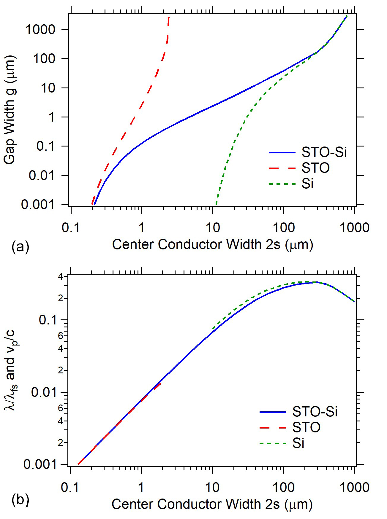
Using this analytical approach with the sample parameters summarized in Table 1, we calculate the value of the gap width that gives a characteristic impedance as a function of the center conductor width . The results of this calculation are shown in figure 3. For comparison, we also show the results for the case with an STO substrate of the same total thickness as well as the case with an Si substrate of the same total thickness. We see that the STO-Si bilayer substrate allows us to achieve a impedance over a much wider range of center conductor widths than either a STO or Si substrate. We found agreement to better than % between the numerical simulations and the analytical calculations provided that a sufficiently fine mesh size was used in the vicinity of the CPW gap. Because of the long times required for accurate simulations, this analytical model can be very useful for initial device design.
| Parameter | Value |
|---|---|
| NbN thickness | nm |
| NbN normal state sheet resistance | /sq |
| NbN critical temperature | 12.0 K |
| NbN sheet kinetic inductance () | pH/sq |
| NbN London penetration depth () | nm |
| NbN Pearl length () | m |
| STO relative permittivity | |
| STO thickness | nm |
| Si relative permittivity | |
| Si thickness | m |
Devices that combine high kinetic inductance superconducting thin films and high permittivity substrates enable the creation of impedance-matched microwave devices in which the signal wavelength and velocity can be reduced by more than two orders of magnitude, as demonstrated by the CPW double-resonator device described in this paper. This extreme wavelength compression facilitates the on-chip integration of many types of distributed microwave devices that would be prohibitively large using conventional material systems, expanding the possibilities for scaling up cryogenic microwave systems.
See the supplementary material for additional details on the STO growth, the experimental setup for device characterization, numerical simulations, and the analytical model.
Acknowledgements.
This work was supported by National Science Foundation grants ECCS-2000778 (UNF) and ECCS-2000743 (MIT). M.C. acknowledges support from the Claude E. Shannon Award.References
- Schoelkopf and Girvin (2008) R. J. Schoelkopf and S. M. Girvin, Nature 451, 664–669 (2008).
- Kjaergaard et al. (2020) M. Kjaergaard, M. E. Schwartz, J. Braumüller, P. Krantz, J. I.-J. Wang, S. Gustavsson, and W. D. Oliver, Ann. Rev. Cond. Mat. Phys. 11, 369–395 (2020).
- Wendin (2017) G. Wendin, Rep. Prog. Phys. 80, 106001 (2017).
- Wollman et al. (2019) E. E. Wollman, V. B. Verma, A. E. Lita, W. H. Farr, M. D. Shaw, R. P. Mirin, and S. W. Nam, Optics Express 27, 35279 (2019).
- Tolpygo (2016) S. K. Tolpygo, Low Temperature Physics 42, 361 (2016).
- Gambetta, Chow, and Steffen (2017) J. M. Gambetta, J. M. Chow, and M. Steffen, npj Quantum Information 3, 2 (2017).
- Hornibrook et al. (2015) J. M. Hornibrook, J. I. Colless, I. D. C. Lamb, S. J. Pauka, H. Lu, A. C. Gossard, J. D. Watson, G. C. Gardner, S. Fallahi, M. J. Manfra, and D. J. Reilly, Phys. Rev. Applied 3, 24010 (2015).
- Brecht et al. (2016) T. Brecht, W. Pfaff, C. Wang, Y. Chu, L. Frunzio, M. H. Devoret, and R. J. Schoelkopf, npj Quantum Information 2, 16002 (2016).
- Seki and Hasegawa (1981) S. Seki and H. Hasegawa, Electron. Lett. 17, 940–941 (1981).
- Chang and Chang (2012) W.-S. Chang and C.-Y. Chang, IEEE Trans. Microwave Theory Tech. 60, 3376–3383 (2012).
- Rosa et al. (2018) A. Rosa, S. Verstuyft, A. Brimont, D. V. Thourhout, and P. Sanchis, Scientific Reports 8, 5672 (2018).
- Annunziata et al. (2010) A. J. Annunziata, D. F. Santavicca, L. Frunzio, G. Catelani, M. J. Rooks, A. Frydman, and D. E. Prober, Nanotechnology 21, 445202 (2010).
- Hazard et al. (2019) T. M. Hazard, A. Gyenis, A. D. Paolo, A. T. Asfaw, S. A. Lyon, A. Blais, and A. A. Houck, Phys. Rev. Lett. 122, 010504 (2019).
- Grünhaupt et al. (2019) L. Grünhaupt, M. Spiecker, D. Gusenkova, N. Maleeva, S. T. Skacel, I. Takmakov, F. Valenti, P. Winkel, H. Rotzinger, W. Wernsdorfer, A. V. Ustinov, and I. M. Pop, Nature Materials 18, 816–819 (2019).
- Santavicca et al. (2016) D. F. Santavicca, J. K. Adams, L. E. Grant, A. N. McCaughan, and K. K. Berggren, J. Appl. Phys. 119, 234302 (2016).
- Colangelo et al. (2021) M. Colangelo, D. Zhu, D. F. Santavicca, B. A. Butters, J. C. Bienfang, and K. K. Berggren, Phys. Rev. Applied 15, 024064 (2021).
- Robertson (2004) J. Robertson, Eur. Phys. J. Appl. Phys. 28, 265–291 (2004).
- Pai et al. (2018) Y.-Y. Pai, A. Tylan-Tyler, P. Irvin, and J. Levy, Rep. Prog. Phys. 81, 036503 (2018).
- Sakudo and Unoki (1971) T. Sakudo and H. Unoki, Phys. Rev. Lett. 26, 851–853 (1971).
- Davidovikj et al. (2017) D. Davidovikj, N. Manca, H. S. J. van der Zant, A. D. Caviglia, and G. A. Steele, Phys. Rev. B 95, 214513 (2017).
- Li et al. (2003) H. Li, X. Hu, Y. Wei, Z. Yu, X. Zhang, R. Droopad, A. A. Demkov, J. Edwards, K. Moore, and W. Ooms, J. Appl. Phys. 93, 4521 (2003).
- Warusawithana et al. (2009) M. P. Warusawithana, C. Cen, C. R. Sleasman, J. C. Woicik, Y. Li, L. F. Kourkoutis, J. A. Klug, H. Li, P. Ryan, L.-P. Wang, M. Bedzyk, D. A. Muller, L.-Q. Chen, J. Levy, and D. G. Schlom, Science 324, 367–370 (2009).
- Guguschev et al. (2015) C. Guguschev, Z. Galazka, D. J. Kok, U. Juda, A. Kwasniewski, and R. Uecker, Cryst. Eng. Comm. 17, 4662 (2015).
- Findikoglu et al. (1995) A. T. Findikoglu, Q. X. Jia, I. H. Campbell, X. D. Wu, D. Reagor, C. B. Mombourquette, and D. McMurry, Appl. Phys. Lett. 66, 3674 (1995).
- M.Adam, D.Fuchs, and R.Schneider (2002) M.Adam, D.Fuchs, and R.Schneider, Physica C: Superconductivity 372–376, 504–507 (2002).
- Kourkoutis et al. (2008) L. F. Kourkoutis, C. S. Hellberg, V. Vaithyanathan, H. Li, M. K. Parker, K. E. Andersen, D. G. Schlom, and D. A. Muller, Phys. Rev. Lett. 100, 036101 (2008).
- Medeiros et al. (2019) O. Medeiros, M. Colangelo, I. Charaev, and K. K. Berggren, J. Vac. Sci. Tech. A 37, 041501 (2019).
- Li et al. (1998) H. C. Li, W. Si, A. D. West, and X. X. Xi, Appl. Phys. Lett. 73, 464 (1998).
- Xi et al. (1999) X. X. Xi, H.-C. Li, W. Si, and A. A. Sirenko, “Nano-crystalline and thin film magnetic oxides,” (Springer, 1999) Chap. Dielectric Properties and Applications of Strontium Titanate Thin Films for Tunable Electronics.
- Gevorgian, Linner, and Kollberg (1995) S. Gevorgian, L. J. P. Linner, and E. L. Kollberg, IEEE Trans. Microwave Theory Tech. 43, 772–779 (1995).
- Garg, Bahl, and Bozzi (2013) R. Garg, I. Bahl, and M. Bozzi, Microstrip Lines and Slotlines, Third Edition (Artech House, Boston, 2013).
- Clem (2013) J. R. Clem, J. Appl. Phys. 113, 013910 (2013).