A scalable network model for electrically tunable ferroelectric domain structure in twistronic bilayers of two-dimensional semiconductors
Abstract
Moiré structures in small-angle-twisted bilayers of two-dimensional (2D) semiconductors with a broken-symmetry interface form arrays of ferroelectric (FE) domains with periodically alternating out-of-plane polarization. Here, we propose a network theory for the tunability of such FE domain structure by applying an electric field perpendicular to the 2D crystal. Using multiscale analysis, we derive a fully parametrized string-theory-like description of the domain wall network (DWN) and show that it undergoes a qualitative change, after the arcs of partial dislocation (PD) like domain walls merge (near the network nodes) into streaks of perfect screw dislocations (PSD), which happens at a threshold displacement field dependent on the DWN period.
Two-dimensional material twistronics, fueled by discoveries of new phenomena in twisted graphene bilayers [1, 2, 3, 4, 5, 6, 7, 8, 9, 10] and trilayers [11, 12, 13, 14, 15, 16], has recently expanded onto a broader range of van der Waals systems [17, 18, 19, 20, 21, 22, 23]. In general, twistronic structures are associated with geometrical moiré patterns: a periodic variation local stacking of the two layers. In long-period moiré patterns, characteristic for small-angle-twisted bilayers, the areas of energetically preferential stacking expand into mesoscale domains [24, 25, 26, 27], embedded into a domain wall network (DWN). In particular, by assembling a homobilayer of two inversion-asymmetric honeycomb monolayers (hBN or transition metal dichalcogenides (TMD)) with parallel orientation of their unit cells, one obtains a triangular array of domains with broken mirror and inversion symmetries [28, 29, 30, 31, 32, 33] and an out-of-plane ferroelectric (FE) polarization [34, 35, 36], which direction alternates between the neighboring XM-stacking domains (metal atoms overlaying chalcogens) and their MX twins (chalcogens over metal atoms) [37, 38].
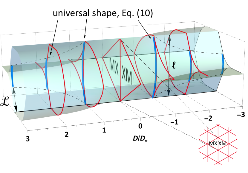
The coupling between the out-of-plane FE polarization and an externally controlled displacement field, , varies the energies of XM and MX, changing the ratio between their areas and leading to the deformation of DWN. Here, we offer a generic theory for the field-tunable FE domain structure in twistronic TMD bilayers, fully quantified with the help of multiscale modelling approach [38, 39, 40, 36] for MX2-bilayers (M=Mo,W; X=S,Se). For weak fields , the continuously deforming domain walls retain their partial dislocation character, however, above the threshold, , pairs of partial dislocations (PD) form streaks of perfect (full) screw dislocations (PSD, of length ) near the network nodes. In Fig. 1, we illustrate how the arcs of XM/MX domain walls with a universal shape merge and split apart upon the variation of , where the threshold field and DWN parameters scale with elastic parameters of a partial dislocation and the DWN period, , as .
The scenario of the DWN transformation in Fig. 1 is a result of the following analysis. First, we use density functional theory (DFT) to quantify the coupling of FE polarization of an asymmetric TMD interface to an external out-of-plane displacement field, . By taking into account the resulting coupling in the competition between the inter-layer adhesion and elastic strain in the layers, which has been used [38] and tested [27] earlier in the studies of mesoscale lattice relaxation in TMD bilayers, we derive an effective theory, formulated in terms of the DWN deformations. Finally, we find an analytical solution for such a ’string-like’ theory, which has a universal form scaling with the ratio.
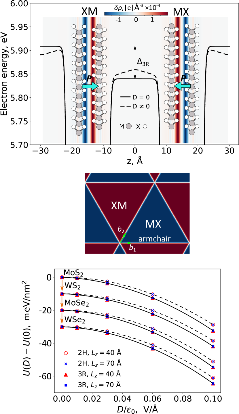
Ab initio modelling of FE bilayers in the out-of-plane electric field. Here, we use two methods to carry out DFT calculations for 3R-bilayers, with the coinciding results. In the first method, we use Quantum ESPRESSO (QE) [41, 42] to construct a supercell with a pair of mirror-reflected (MX and XM) bilayers, separated by a large vacuum gap, as shown in Fig. 2. This choice of the structure eliminates an issue with periodic boundary condition for potential of the FE charges [36]. In the second method we construct a single 3R-bilayer and use Coulomb truncation in the out-of-plane direction [43] with QE and dipole-correction with VASP[44]. An example of the computed charge transfer, , between the layers of an individual bilayer (which integral, , determines the areal density of the FE dipole moment) and a potential drop, , across the double charge layer, is shown in Fig. 2. To mention, the computed values of and are related as , in agreement with the earlier studies of 3D bulk FE materials [45].
The displacement field, accounted for by adding a triangular potential, , to the input pseudo-potentials, produces a shift, of the bilayer energy. The latter includes a linear term, accounting for the FE polarization, and a quadratic downward shift due to the dielectric out-of-plane polarizability of the material:
| (1) |
Here, we parametrise the coupling by a dimensionless parameter and the out-of-plane dielectric polarizability by (where is the unit cell area of a TMD monolayer). The DFT-computed energies of bilayers of four different TMDs are shown in Fig. 2: in this computation, we used two different supercell periods (40 Å and 70 Å, which set the length of the vacuum spacer). Using Eq. (1), we find the polarizability values, which are very close to polarizability, , computed for the inversion-symmetric 2H bilayer111For monolayers and 2H-bilayers we used the Coulomb truncation in the out-of-plane direction[43].. When recalculated per monolayer, these values also agree with the separately computed monolayer polarizability, (, see in Table 1). This confirms that the dielectric response of a wide band gap van der Waals materials is determined by the intra-layer polarization of the constituent atoms 222 Unlike Refs. [55, 56], which use -averaged electric field for computation of dielectric permitivities of bilayers, we express the quadratic amendment to the total energy via out-of-plane displacement field, conserving across every cross-section of the structure. This allows us to avoid uncertainties in , which may appear at averaging of the electric field in crystals with a few out-of-plane unit cells [45]. We find that the polarizability, computed for a TMD monolayer, its 2H and 3R bilayer, and thicker 2H films, linearly scales with with the number of layers. This observation contradicts some earlier DFT studies of dielectric susceptibility of TMDs [55, 56] which claimed a pronounce layer-number-dependence, but agrees with the more recent results [49] published by some of the authors of Refs [55]. . These values enabled us to estimate the -axis dielectric susceptibility of bulk TMD crystals [48, 49, 50], , arriving at the values in the range of , listed in Table 1.
Despite a substantial polarizability of monolayers, the data in Fig. 2 are described well by Eq. (1) with , pointing towards a decoupling of the inter-layer FE charge transfer from the intra-layer dielectric polarizability. Moreover, by comparing the DFT-computed values of the double-layer potential drop to the FE coupling with the displacement field, , in Eq. (2), we find that the linear in energy shift in MX and XM domains (which have opposite out-of-plane FE polarization, , and voltage drop across the double charge layer, ) can be described very well as 333The expression for interaction energy of the FE polarization with displacement field naturally comes when assuming a local dielectric permittivity in a continuum medium approximation. Indeed, suppose the FE charges, with plane-averaged density , are placed in the medium with local dielectric permittivity . From the Poisson equation and electro-neutrality condition , we express the potential drop across the layer of charges as . At the same time, interaction energy of these charges with uniform external out-of-plane displacement field (related to local electric field as ) reads as . After changing variables, , at the last step of that calculation, we arrive at the relation in Eq. (2).
| (2) |
Below, we will use this coupling to model tunability of the DWN by displacement field.
| , | , | , | ||||||
|---|---|---|---|---|---|---|---|---|
| Å3 | Å3 | Å3 | mV | mV | nm-1 | |||
| MoS2 | 89.89 | 89.80 | 44.46 | 6.45 | 1.03 | 68 | 16.4 | 22.152 |
| 89.93 | 89.85 | 44.48 | 6.48 | 1.02 | ||||
| WS2 | 88.43 | 88.37 | 43.95 | 5.95 | 1.00 | 62 | 15 | 22.598 |
| 88.43 | 88.37 | 43.94 | 5.95 | 1.00 | ||||
| MoSe2 | 105.32 | 105.22 | 52.29 | 7.65 | 1.05 | 66 | 15.7 | 20.520 |
| 105.31 | 105.25 | 52.24 | 7.67 | 1.07 | ||||
| WSe2 | 104.37 | 104.33 | 52.03 | 7.39 | 1.04 | 65 | 15.3 | 20.953 |
| 104.32 | 104.28 | 51.97 | 7.32 | 1.07 |
-
For , and we show the values obtained with QE (top row) and - for comparison - with VASP (bottom row). For QE we used full-relativistic ultra-soft pseudo-potentials and a plane-wave cutoff energy of 70 Ry. For VASP, we used PAW full-relativistic pseudo-potentials and 60 Ry cut-off (with a -point grid and a Perdew-Burke-Ernzerhof (PBE)[52] exchange-correlation functional for both QE and VASP).
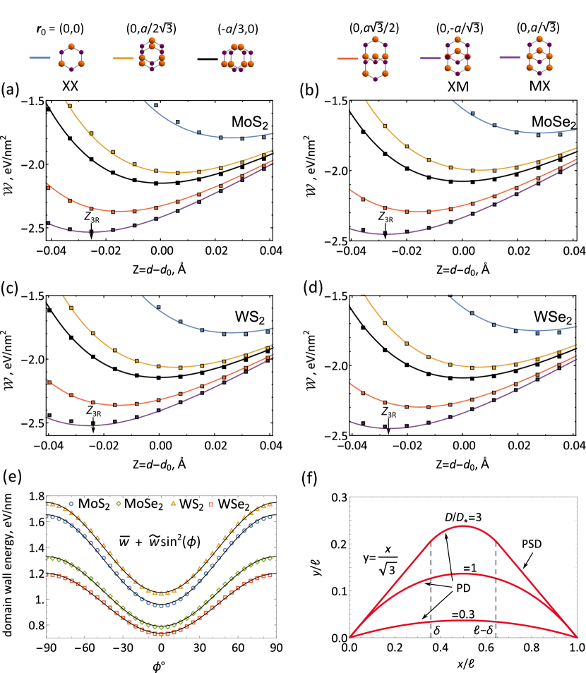
Mesoscale model for lattice reconstruction is formulated in terms of the bilayer energy dependence on local stacking of the two layers and their strain [27, 38, 39], incorporated via an interlayer offset, , which varies across the superlattice, as prescribed by a small-angle, , misalignment between the top (t) and bottom (b) crystals and their elastic deformations, . Locally, stacking determines the interlayer distance, which corresponds to the minimum of the stacking-dependent adhesion energy, , quantified for the four TMDs using DFT modelling and displayed in Fig. 3. For convenience, the inter-layer distance () dependence of the computed is shown as a function of , counted from the minimum (at ) of the offset-averaged adhesion energy, which coincides with (one of stacking configurations shown in Fig. 3). As a result, energy density, characterizing the relaxation functional, reads:
| (3) | ||||
Here, the first term accounts for strain, ( and are the monolayer elastic moduli). The second term describes adhesion energy between top and bottom layers, where determines curvature of the adhesion energy of 3R-stacked bilayers, which characterises frequency of layer breathing mode [38], and is the first star of reciprocal lattice vectors of TMD monolayer, (for details, see Refs. [27, 38, 39]). The last term is responsible for the energy shift due to the external field.
The next steps in the analysis require choosing an optimal interlayer distance between the two monolayer, which depends on the encapsulation environment of the bilayer. For a bilayer in vacuum, or encapsulated into a soft flexible matrix with a weaker adhesion to TMD than the the interlayer adhesion , we find from Eq. (A scalable network model for electrically tunable ferroelectric domain structure in twistronic bilayers of two-dimensional semiconductors) that, locally, . For a strong substrate-TMD coupling, the monolayers would remain flat, and the optimal interlayer distance would be across the entire moiŕe pattern. For either of these two cases, we substitute the corresponding choice of in Eq. (A scalable network model for electrically tunable ferroelectric domain structure in twistronic bilayers of two-dimensional semiconductors), and also into the local voltage drop across the double layer of charge (in the last term in Eq. (A scalable network model for electrically tunable ferroelectric domain structure in twistronic bilayers of two-dimensional semiconductors)) corresponding to the local stacking configuration, which form has been established earlier [36]:
For XM and MX stackings, this gives , which values, taken from the recent ab initio simulations [40, 38], are listed in Table 2.
| , | , | , | , | , | , | , | ||||
|---|---|---|---|---|---|---|---|---|---|---|
| eV/nm2 | eV/nm3 | eV/nm4 | N/m | N/m | nm | nm | eV/nm | eV/nm | eV/nm | |
| MoS2 | 0.189 | 5.634 | 214 | 70.9 | 83.2 | 0.316 | 0.636 | 0.96 | 0.69 | 2.24 |
| WS2 | 0.212 | 6.327 | 213 | 72.5 | 52.5 | 0.315 | 0.638 | 1.05 | 0.69 | 2.45 |
| MoSe2 | 0.1975 | 5.707 | 189 | 49.6 | 42.3 | 0.329 | 0.670 | 0.79 | 0.54 | 1.84 |
| WSe2 | 0.1514 | 4.381 | 190 | 48.4 | 29.7 | 0.328 | 0.671 | 0.74 | 0.46 | 1.69 |
Network model. While the minimization of the energy functional in (A scalable network model for electrically tunable ferroelectric domain structure in twistronic bilayers of two-dimensional semiconductors) enables one to find all mesoscale details of the lattice adjustments of the two crystalline plane of the bilayer, it is more practical to use another method for the analysis of small-angle () twisted bilayers. This is because, in the latter case, most of the areas of the moiré pattern is occupied by the homogeneous MX and XM stacking domains with a characteristic size of nm, whereas the deformations are concentrated inside narrow domain walls, which are only only few nanometres in width [38, 27]. Then, we define the DWN energy,
by subtracting the energy of a uniform MX-stacked bilayer at from in Eq. (A scalable network model for electrically tunable ferroelectric domain structure in twistronic bilayers of two-dimensional semiconductors). This reduces the problem to the analysis of , where we can treat each domain wall as a string, characterised by energy per unit length dependent on a crystallographic orientation of the domain wall axis [38], with - as shown in Fig. 3(e) - a pronounced minimum at the armchair direction in the TMD crystal.
A finite displacement field acts as an external drive for increasing areas of domains with the preferential ferroelectric polarization. This leads to the bending of the partial dislocation (PD) domain walls, hence, increasing their energy due to their elongation and the PD axis deviation from the armchair axis. The exact form on the deformed DWN can be found by solving a ’string theory’ model, expressed in terms of a deflection, , of PD segments from the closest armchair direction, formalised using an energy functional,
| (4) |
Here, the first term in the integral describes the orientation-dependence of the PD energy, , and its stretching, accounted by a factor with standing for an angle between the dislocation axis and the closest armchair direction in the crystal, so that . Two ’stiffness’ parameters, and , were determined using the data from Ref. [38], see Table 2 for their values for various TMDs. The second term in the integral stands for the energy gain from a bigger area of the energetically preferential FE polarization domain. The last two terms in accounts for two PDs merging, near each DWN node, into streaks of PSDs with a length (projected onto and intervals), which energetically preferable orientation is along zigzag axis in the crystal and energy per unit length is (Table 2).
Using variational principle, we obtain an equation for the the shape of each string,
| (5) |
where appears as an additional variable. Note that zero values of at the network nodes requires vanishing of derivative in the middle of interval, i.e. providing a symmetrical shape of the PD, with .
For a small , energetically favourable domains grow due to bending of PDs, with their ends fixed at network nodes, . This elastic stretching has no threshold in and the string form is described by 444At small (when ) approximate solution of Eq. (5) is given by parabola: .,
| (6) |
where is a real root of
| (7) |
Note that and that for .
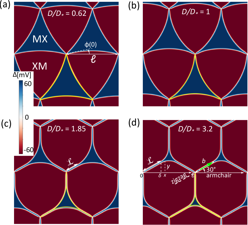
Bending, described by Eq. (6), takes a new qualitative form after each pair of PDs near the network nodes () touch each other, see Fig. 4(j). This condition corresponds to (i.e., ), which, together with Eq. (6) determines a threshold displacement field,
| (8) | ||||
It is important to note that pairs of touching PDs cannot annihilate, as a sum of their Burgers vectors (, , ) corresponds to the Burgers vector () of a PSD, required to maintain an overall twist between two monolayers in the bilayer. This means that they actually form streaks of PSDs, which lengths grow with a further increase of the electric drive, as
| (9) |
The latter scaling law follows from the solution of Eq. (5) on the interval with the boundary conditions, , where is a projection of onto the -axis. Hence, above the threshold, DWN is composed of (A) PSD streaks near each network node aligned with zigzag directions in TMD, and separating the adjacent expanded energetically favourable 3R-domains and (B) PD arcs splitting up at the PSD ends, and , and touching each other at the splitting points.
To find the shape of the remaining PD arcs for any , we rewrite Eq. (5) in dimensionless coordinates, and defined by , ,
Its solution has the same structure for any ,
| (10) | |||
describing the universal shape of partial dislocation arcs, scaled by the ratio , as shown in Fig. 3(f).
Finally, to validate the accuracy of the obtained analytical solution, obtained using the network model, we also performed the mesoscale lattice relaxation for a MoS2 bilayer with a interlayer twist (corresponding to nm), by minimising the full energy functional in Eq. (A scalable network model for electrically tunable ferroelectric domain structure in twistronic bilayers of two-dimensional semiconductors). For this, we analysed the Euler-Lagrange equations for the displacement fields , obtained by applying variational principle to . We solved those numerically, seeking for periodic (with the the period ) solutions on a sufficiently dense grid using interior point method implemented in GEKKO Optimization Suite package [54]. The computed fields were used to obtain the local values of the inter-layer offset, , which we substituted into Eqs. (A scalable network model for electrically tunable ferroelectric domain structure in twistronic bilayers of two-dimensional semiconductors) to find the interlayer distance, , and to map the interlayer potential drop across the domain structure. The results for the latter quantity are shown in Fig. 4 for various values of displacement field, displaying a close agreement with the analytical solution of the network model shown by yellow lines.
To conclude, the developed effective network model gives an efficient description of the long-period domain structure in small-angle-twisted TMD bilayers with ferroelectric interface and its deformation by an out-of-plane electric field. Its analytical solution in Eqs. (6) - (10) gives a simple tool for the interpretation of experimentally measured variations of the domains’ shapes, such as in the recently studied bilayers with ferroelectric properties [30, 29, 31, 32, 33].
Acknowledgments. We thank Andre Geim, Roman Gorbachev, Philip Kim, and David Vanderbilt for useful discussions. This study has been supported by the European Graphene Flagship Core3 Project, EU Quantum Flagship Project 2D-SIPC, and EPSRC grants P/W006502/1, EP/V007033/1, EP/S030719/1. The reported ab initio simulations were performed using EPSRC ARCHER facility and the University of Manchester CSF.
References
- Cao et al. [2018a] Y. Cao, V. Fatemi, S. Fang, K. Watanabe, T. Taniguchi, E. Kaxiras, and P. Jarillo-Herrero, Unconventional superconductivity in magic-angle graphene superlattices, Nature 556, 43 (2018a).
- Cao et al. [2018b] Y. Cao, V. Fatemi, A. Demir, S. Fang, S. L. Tomarken, J. Y. Luo, J. D. Sanchez-Yamagishi, K. Watanabe, T. Taniguchi, E. Kaxiras, and et al, Correlated insulator behaviour at half-filling in magic-angle graphene superlattices, Nature 556, 80 (2018b).
- Yankowitz et al. [2019] M. Yankowitz, S. Chen, H. Polshyn, Y. Zhang, K. Watanabe, T. Taniguchi, D. Graf, A. F. Young, and C. R. Dean, Tuning superconductivity in twisted bilayer graphene, Science 363, 1059 (2019).
- Lu et al. [2019] X. Lu, P. Stepanov, W. Yang, M. Xie, M. A. Aamir, I. Das, C. Urgell, K. Watanabe, T. Taniguchi, G. Zhang, et al., Superconductors, orbital magnets and correlated states in magic-angle bilayer graphene, Nature 574, 653 (2019).
- Sharpe et al. [2019] A. L. Sharpe, E. J. Fox, A. W. Barnard, J. Finney, K. Watanabe, T. Taniguchi, M. Kastner, and D. Goldhaber-Gordon, Emergent ferromagnetism near three-quarters filling in twisted bilayer graphene, Science 365, 605 (2019).
- Cao et al. [2021] Y. Cao, D. Rodan-Legrain, J. M. Park, N. F. Yuan, K. Watanabe, T. Taniguchi, R. M. Fernandes, L. Fu, and P. Jarillo-Herrero, Nematicity and competing orders in superconducting magic-angle graphene, Science 372, 264 (2021).
- Kerelsky et al. [2021] A. Kerelsky, C. Rubio-Verdú, L. Xian, D. M. Kennes, D. Halbertal, N. Finney, L. Song, S. Turkel, L. Wang, K. Watanabe, T. Taniguchi, J. Hone, C. Dean, D. N. Basov, A. Rubio, and A. N. Pasupathy, Moiréless correlations in abca graphene, PNAS 118 (2021).
- Xu et al. [2019] S. G. Xu, A. I. Berdyugin, P. Kumaravadivel, F. Guinea, R. Krishna Kumar, D. A. Bandurin, S. V. Morozov, W. Kuang, B. Tsim, S. Liu, J. H. Edgar, I. V. Grigorieva, V. I. Fal’ko, M. Kim, and A. K. Geim, Giant oscillations in a triangular network of one-dimensional states in marginally twisted graphene, Nature Communications 10, 4008 (2019).
- Gadelha et al. [2021] A. C. Gadelha, D. A. A. Ohlberg, C. Rabelo, E. G. S. Neto, T. L. Vasconcelos, J. L. Campos, J. S. Lemos, V. Ornelas, D. Miranda, R. Nadas, F. C. Santana, K. Watanabe, T. Taniguchi, B. van Troeye, M. Lamparski, V. Meunier, V.-H. Nguyen, D. Paszko, J.-C. Charlier, L. C. Campos, L. G. Cançado, G. Medeiros-Ribeiro, and A. Jorio, Localization of lattice dynamics in low-angle twisted bilayer graphene, Nature 590, 405 (2021).
- Kazmierczak et al. [2021] N. P. Kazmierczak, M. Van Winkle, C. Ophus, K. C. Bustillo, S. Carr, H. G. Brown, J. Ciston, T. Taniguchi, K. Watanabe, and D. K. Bediako, Strain fields in twisted bilayer graphene, Nature Materials 20, 956 (2021).
- Polshyn et al. [2020] H. Polshyn, J. Zhu, M. A. Kumar, Y. Zhang, F. Yang, C. L. Tschirhart, M. Serlin, K. Watanabe, T. Taniguchi, A. H. MacDonald, et al., Electrical switching of magnetic order in an orbital chern insulator, Nature 588, 66 (2020).
- Xu et al. [2021] S. Xu, M. M. Al Ezzi, N. Balakrishnan, A. Garcia-Ruiz, B. Tsim, C. Mullan, J. Barrier, N. Xin, B. A. Piot, T. Taniguchi, K. Watanabe, A. Carvalho, A. Mishchenko, A. K. Geim, V. I. Fal’ko, S. Adam, A. H. C. Neto, K. S. Novoselov, and Y. Shi, Tunable van hove singularities and correlated states in twisted monolayer–bilayer graphene, Nature Physics 17, 619 (2021).
- Chen et al. [2019] G. Chen, L. Jiang, S. Wu, B. Lyu, H. Li, B. L. Chittari, K. Watanabe, T. Taniguchi, Z. Shi, J. Jung, Y. Zhang, and F. Wang, Evidence of a gate-tunable mott insulator in a trilayer graphene moiré superlattice, Nature Physics 15, 237 (2019).
- Shen et al. [2020] C. Shen, Y. Chu, Q. Wu, N. Li, S. Wang, Y. Zhao, J. Tang, J. Liu, J. Tian, K. Watanabe, et al., Correlated states in twisted double bilayer graphene, Nature Physics 16, 520 (2020).
- Chen et al. [2021] S. Chen, M. He, Y.-H. Zhang, V. Hsieh, Z. Fei, K. Watanabe, T. Taniguchi, D. H. Cobden, X. Xu, C. R. Dean, et al., Electrically tunable correlated and topological states in twisted monolayer–bilayer graphene, Nature Physics 17, 374 (2021).
- Park et al. [2021] J. M. Park, Y. Cao, K. Watanabe, T. Taniguchi, and P. Jarillo-Herrero, Tunable strongly coupled superconductivity in magic-angle twisted trilayer graphene, Nature 590, 249 (2021).
- Kunstmann et al. [2018] J. Kunstmann, F. Mooshammer, P. Nagler, A. Chaves, F. Stein, N. Paradiso, G. Plechinger, C. Strunk, C. Schüller, G. Seifert, and et al, Momentum-space indirect interlayer excitons in transition-metal dichalcogenide van der Waals heterostructures, Nature Physics 14, 801 (2018).
- Rivera et al. [2018] P. Rivera, H. Yu, K. L. Seyler, N. P. Wilson, W. Yao, and X. Xu, Interlayer valley excitons in heterobilayers of transition metal dichalcogenides, Nature Nanotechnology 13, 1004 (2018).
- Nayak et al. [2017] P. K. Nayak, Y. Horbatenko, S. Ahn, G. Kim, J.-U. Lee, K. Y. Ma, A.-R. Jang, H. Lim, D. Kim, S. Ryu, and et al, Probing evolution of twist-angle-dependent interlayer excitons in MoSe2/WSe2 van der Waals heterostructures, ACS Nano 11, 4041 (2017).
- Alexeev et al. [2019] E. M. Alexeev, D. A. Ruiz-Tijerina, M. Danovich, M. J. Hamer, D. J. Terry, P. K. Nayak, S. Ahn, S. Pak, J. Lee, J. I. Sohn, and et al, Resonantly hybridized excitons in moiré superlattices in van der Waals heterostructures, Nature 567, 81 (2019).
- McGilly et al. [2020] L. J. McGilly, A. Kerelsky, N. R. Finney, K. Shapovalov, E.-M. Shih, A. Ghiotto, Y. Zeng, S. L. Moore, W. Wu, Y. Bai, K. Watanabe, T. Taniguchi, M. Stengel, L. Zhou, J. Hone, X. Zhu, D. N. Basov, C. Dean, C. E. Dreyer, and A. N. Pasupathy, Visualization of moiré superlattices, Nature Nanotechnology 15, 580 (2020).
- Zhang et al. [2020] Z. Zhang, Y. Wang, K. Watanabe, T. Taniguchi, K. Ueno, E. Tutuc, and B. J. LeRoy, Flat bands in twisted bilayer transition metal dichalcogenides, Nature Physics 16, 1093 (2020).
- Wang et al. [2020] L. Wang, E.-M. Shih, A. Ghiotto, L. Xian, D. A. Rhodes, C. Tan, M. Claassen, D. M. Kennes, Y. Bai, B. Kim, K. Watanabe, T. Taniguchi, X. Zhu, J. Hone, A. Rubio, A. N. Pasupathy, and C. R. Dean, Correlated electronic phases in twisted bilayer transition metal dichalcogenides, Nature Materials 19, 861 (2020).
- Alden et al. [2013] J. S. Alden, A. W. Tsen, P. Y. Huang, R. Hovden, L. Brown, J. Park, D. A. Muller, and P. L. McEuen, Strain solitons and topological defects in bilayer graphene, PNAS 110, 11256 (2013).
- Yoo et al. [2019] H. Yoo, R. Engelke, S. Carr, S. Fang, K. Zhang, P. Cazeaux, S. H. Sung, R. Hovden, A. W. Tsen, T. Taniguchi, and et al, Atomic and electronic reconstruction at the van der Waals interface in twisted bilayer graphene, Nature materials 18, 448 (2019).
- Rosenberger et al. [2020] M. R. Rosenberger, H.-J. Chuang, M. Phillips, V. P. Oleshko, K. M. McCreary, S. V. Sivaram, C. S. Hellberg, and B. T. Jonker, Twist angle-dependent atomic reconstruction and moiré patterns in transition metal dichalcogenide heterostructures, ACS Nano 14, 4550 (2020).
- Weston et al. [2020] A. Weston, Y. Zou, V. Enaldiev, A. Summerfield, N. Clark, V. Zólyomi, A. Graham, C. Yelgel, S. Magorrian, M. Zhou, J. Zultak, D. Hopkinson, A. Barinov, T. H. Bointon, A. Kretinin, N. R. Wilson, P. H. Beton, V. I. Fal’ko, S. J. Haigh, and R. Gorbachev, Atomic reconstruction in twisted bilayers of transition metal dichalcogenides, Nature Nanotechnology 15, 592 (2020).
- Sung et al. [2020] J. Sung, Y. Zhou, G. Scuri, V. Zólyomi, T. I. Andersen, H. Yoo, D. S. Wild, A. Y. Joe, R. J. Gelly, H. Heo, S. J. Magorrian, D. Bérubé, A. M. M. Valdivia, T. Taniguchi, K. Watanabe, M. D. Lukin, P. Kim, V. I. Fal’ko, and H. Park, Broken mirror symmetry in excitonic response of reconstructed domains in twisted MoSe2/MoSe2 bilayers, Nature Nanotechnology 15, 750 (2020).
- Woods et al. [2021] C. Woods, P. Ares, H. Nevison-Andrews, M. Holwill, R. Fabregas, F. Guinea, A. Geim, K. Novoselov, N. Walet, and L. Fumagalli, Charge-polarized interfacial superlattices in marginally twisted hexagonal boron nitride, Nature communications 12, 1 (2021).
- Yasuda et al. [2021] K. Yasuda, X. Wang, K. Watanabe, T. Taniguchi, and P. Jarillo-Herrero, Stacking-engineered ferroelectricity in bilayer boron nitride, Science 372, 1458 (2021).
- Stern et al. [2021] M. V. Stern, Y. Waschitz, W. Cao, I. Nevo, K. Watanabe, T. Taniguchi, E. Sela, M. Urbakh, O. Hod, and M. B. Shalom, Interfacial ferroelectricity by van der Waals sliding, Science 372, 1462 (2021).
- Weston et al. [2021] A. Weston, E. G. Castanon, V. Enaldiev, F. Ferreira, S. Bhattacharjee, S. Xu, H. Corte-Leon, Z. Wu, N. Clark, A. Summerfield, et al., Interfacial ferroelectricity in marginally twisted 2D semiconductors, arXiv:2108.06489 (2021).
- Wang et al. [2021] X. Wang, K. Yasuda, Y. Zhang, S. Liu, K. Watanabe, T. Taniguchi, J. Hone, L. Fu, and P. Jarillo-Herrero, Interfacial ferroelectricity in rhombohedral-stacked bilayer transition metal dichalcogenides, arXiv:2108.07659 (2021).
- Li and Wu [2017] L. Li and M. Wu, Binary compound bilayer and multilayer with vertical polarizations: two-dimensional ferroelectrics, multiferroics, and nanogenerators, ACS Nano 11, 6382 (2017).
- Tong et al. [2020] Q. Tong, M. Chen, F. Xiao, H. Yu, and W. Yao, Interferences of electrostatic moiré potentials and bichromatic superlattices of electrons and excitons in transition metal dichalcogenides, 2D Materials 8, 025007 (2020).
- Ferreira et al. [2021a] F. Ferreira, V. V. Enaldiev, V. I. Fal’ko, and S. J. Magorrian, Weak ferroelectric charge transfer in layer-asymmetric bilayers of 2D semiconductors, Scientific Reports 11, 13422 (2021a).
- Carr et al. [2018] S. Carr, D. Massatt, S. B. Torrisi, P. Cazeaux, M. Luskin, and E. Kaxiras, Relaxation and domain formation in incommensurate two-dimensional heterostructures, Phys. Rev. B 98, 224102 (2018).
- Enaldiev et al. [2020] V. V. Enaldiev, V. Zólyomi, C. Yelgel, S. J. Magorrian, and V. I. Fal’ko, Stacking domains and dislocation networks in marginally twisted bilayers of transition metal dichalcogenides, Phys. Rev. Lett. 124, 206101 (2020).
- Enaldiev et al. [2021] V. V. Enaldiev, F. Ferreira, S. J. Magorrian, and V. I. Fal’ko, Piezoelectric networks and ferroelectric domains in twistronic superlattices in WS2/MoS2 and WSe2/MoSe2 bilayers, 2D Materials 8, 025030 (2021).
- Ferreira et al. [2021b] F. Ferreira, S. J. Magorrian, V. V. Enaldiev, D. A. Ruiz-Tijerina, and V. I. Fal’ko, Band energy landscapes in twisted homobilayers of transition metal dichalcogenides, Applied Physics Letters 118, 241602 (2021b).
- Giannozzi et al. [2009] P. Giannozzi, S. Baroni, N. Bonini, M. Calandra, R. Car, C. Cavazzoni, D. Ceresoli, G. L. Chiarotti, M. Cococcioni, I. Dabo, A. D. Corso, S. de Gironcoli, S. Fabris, G. Fratesi, R. Gebauer, U. Gerstmann, C. Gougoussis, A. Kokalj, M. Lazzeri, L. Martin-Samos, N. Marzari, F. Mauri, R. Mazzarello, S. Paolini, A. Pasquarello, L. Paulatto, C. Sbraccia, S. Scandolo, G. Sclauzero, A. P. Seitsonen, A. Smogunov, P. Umari, and R. M. Wentzcovitch, QUANTUM ESPRESSO: a modular and open-source software project for quantum simulations of materials, Journal of Physics: Condensed Matter 21, 395502 (2009).
- Giannozzi et al. [2017] P. Giannozzi, O. Andreussi, T. Brumme, O. Bunau, M. B. Nardelli, M. Calandra, R. Car, C. Cavazzoni, D. Ceresoli, M. Cococcioni, N. Colonna, I. Carnimeo, A. D. Corso, S. de Gironcoli, P. Delugas, R. A. DiStasio, A. Ferretti, A. Floris, G. Fratesi, G. Fugallo, R. Gebauer, U. Gerstmann, F. Giustino, T. Gorni, J. Jia, M. Kawamura, H.-Y. Ko, A. Kokalj, E. Küçükbenli, M. Lazzeri, M. Marsili, N. Marzari, F. Mauri, N. L. Nguyen, H.-V. Nguyen, A. O. de-la Roza, L. Paulatto, S. Poncé, D. Rocca, R. Sabatini, B. Santra, M. Schlipf, A. P. Seitsonen, A. Smogunov, I. Timrov, T. Thonhauser, P. Umari, N. Vast, X. Wu, and S. Baroni, Advanced capabilities for materials modelling with quantum ESPRESSO, Journal of Physics: Condensed Matter 29, 465901 (2017).
- Sohier et al. [2017] T. Sohier, M. Calandra, and F. Mauri, Density functional perturbation theory for gated two-dimensional heterostructures: Theoretical developments and application to flexural phonons in graphene, Phys. Rev. B 96, 075448 (2017).
- Kresse and Furthmüller [1996] G. Kresse and J. Furthmüller, Efficient iterative schemes for ab initio total-energy calculations using a plane-wave basis set, Physical Review B 54, 11169 (1996).
- Meyer and Vanderbilt [2001] B. Meyer and D. Vanderbilt, Ab initio study of BaTiO3 and PbTiO3 surfaces in external electric fields, Phys. Rev. B 63, 205426 (2001).
- Note [1] For monolayers and 2H-bilayers we used the Coulomb truncation in the out-of-plane direction[43].
- Note [2] Unlike Refs. [55, 56], which use -averaged electric field for computation of dielectric permitivities of bilayers, we express the quadratic amendment to the total energy via out-of-plane displacement field, conserving across every cross-section of the structure. This allows us to avoid uncertainties in , which may appear at averaging of the electric field in crystals with a few out-of-plane unit cells [45]. We find that the polarizability, computed for a TMD monolayer, its 2H and 3R bilayer, and thicker 2H films, linearly scales with with the number of layers. This observation contradicts some earlier DFT studies of dielectric susceptibility of TMDs [55, 56] which claimed a pronounce layer-number-dependence, but agrees with the more recent results [49] published by some of the authors of Refs [55].
- Slizovskiy et al. [2019] S. Slizovskiy, A. Garcia-Ruiz, A. I. Berdyugin, N. Xin, T. Taniguchi, K. Watanabe, A. K. Geim, N. D. Drummond, and V. I. Fal’ko, Out-of-plane dielectric susceptibility of graphene in twistronic and bernal bilayers, arXiv:1912.10067 (2019).
- Tian et al. [2020] T. Tian, D. Scullion, D. Hughes, L. H. Li, C.-J. Shih, J. Coleman, M. Chhowalla, and E. J. G. Santos, Electronic polarizability as the fundamental variable in the dielectric properties of two-dimensional materials, Nano Letters 20, 841 (2020).
- Slizovskiy et al. [2021] S. Slizovskiy, A. Garcia-Ruiz, A. I. Berdyugin, N. Xin, T. Taniguchi, K. Watanabe, A. K. Geim, N. D. Drummond, and V. I. Fal’ko, Out-of-plane dielectric susceptibility of graphene in twistronic and bernal bilayers, Nano Letters 21, 6678 (2021).
- Note [3] The expression for interaction energy of the FE polarization with displacement field naturally comes when assuming a local dielectric permittivity in a continuum medium approximation. Indeed, suppose the FE charges, with plane-averaged density , are placed in the medium with local dielectric permittivity . From the Poisson equation and electro-neutrality condition , we express the potential drop across the layer of charges as . At the same time, interaction energy of these charges with uniform external out-of-plane displacement field (related to local electric field as ) reads as . After changing variables, , at the last step of that calculation, we arrive at the relation in Eq. (2\@@italiccorr).
- Perdew and Zunger [1981] J. P. Perdew and A. Zunger, Self-interaction correction to density-functional approximations for many-electron systems, Phys. Rev. B 23, 5048 (1981).
- Note [4] At small (when ) approximate solution of Eq. (5\@@italiccorr) is given by parabola: .
- Beal et al. [2018] L. D. Beal, D. C. Hill, R. A. Martin, and J. D. Hedengren, Gekko optimization suite, Processes 6, 106 (2018).
- Santos and Kaxiras [2013] E. J. Santos and E. Kaxiras, Electrically driven tuning of the dielectric constant in MoS2 layers, ACS Nano 7, 10741 (2013).
- Laturia et al. [2020] A. Laturia, M. L. Van de Put, and W. G. Vandenberghe, Dielectric properties of hexagonal boron nitride and transition metal dichalcogenides: from monolayer to bulk, npj 2D Materials and Applications 4, 28 (2020).