Supercurrent diode effect and magnetochiral anisotropy in few-layer NbSe2
Abstract
Nonreciprocal transport refers to charge transfer processes that are sensitive to the bias polarity. Until recently, nonreciprocal transport was studied only in dissipative systems, where the nonreciprocal quantity is the resistance. Recent experiments have, however, demonstrated nonreciprocal supercurrent leading to the observation of a supercurrent diode effect in Rashba superconductors, opening the vision of dissipationless electronics. Here we report on a supercurrent diode effect in NbSe2 constrictions obtained by patterning NbSe2 flakes with both even and odd layer number. The observed rectification is driven by valley-Zeeman spin-orbit interaction. We demonstrate a rectification efficiency as large as 60%, considerably larger than the efficiency of devices based on Rashba superconductors. In agreement with recent theory for superconducting transition metal dichalcogenides, we show that the effect is driven by an out-of-plane magnetic field component. Remarkably, we find that the effect becomes field-asymmetric in the presence of an additional in-plane field component transverse to the current direction. Supercurrent diodes offer a further degree of freedom in designing superconducting quantum electronics with the high degree of integrability offered by van der Waals materials.
The archetypal example of a nonreciprocal electronic device is the diode. The term nonreciprocity in this context is used to imply a large difference in resistance between opposite bias polarities. For a conventional semiconductor diode, nonreciprocity follows from the inequivalence of the two crystals forming the junction, which have different types of doping. In homogeneous devices, polarity-dependent resistance is observed when both inversion and time-reversal symmetry are broken simultaneously. As shown by Rikken et al. [1, 2], in noncentrosymmetric conductors nonreciprocal resistance can be phenomenologically described by
| (1) |
where the coefficient refers to the usual magnetoresistance and is the magnetochiral anisotropy (MCA) coefficient. In normal conductors, is typically very small. Its strength is, in fact, determined by the ratio between spin-orbit perturbation and the Fermi energy. Nonreciprocal transport therefore becomes discernible in semiconductors with low Fermi level and large spin-orbit interaction (SOI) [3]. The MCA effect can be greatly amplified in noncentrosymmetric superconductors [4, 5, 6, 7, 8, 6]. Here, the energy scale governing the fluctuation regime close to the critical temperature is not the Fermi energy, but the superconducting gap. Another way to boost MCA for the resistance is to engineer nonreciprocal vortex motion in a superconductor by asymmetric patterning of artificial pinning centers [9].
In the past years, superconductivity-enhanced MCA for the resistance has been studied extensively. There is a satisfactory understanding of the mechanisms producing nonreciprocal resistance and theory predictions successfully describe the experiments [10, 11]. On this basis, some first applications, such as superconducting antenna rectifiers [8] or spin filtering diodes [12], have already been proposed.
Until recently, studies on nonreciprocal transport, even when exploiting superconductivity to enhance MCA, have focused exclusively on resistance. The seminal demonstration of a dissipationless nonreciprocal supercurrent [16] was only recently provided by experiments on synthetic Rashba superconductors based on Nb/V/Ta multilayers [17] and on Josephson junctions [18] with strong Rashba SOI. Such a nonreciprocal supercurrent gives rise to the so-called superconducting diode effect, where the supercurrent can flow only in one direction that can be switched by a magnetic field 111Since the terminology has not settled yet in the literature, it is possible to find the term superconducting diode effect referred to resistance MCA, when this latter is enhanced by superconducting fluctuation near the critical temperature. Here, we refer exclusively to the (dissipationless) supercurrent diode effect..
The MCA for the electrical resistance and that for the superflow are two clearly distinct effects. The latter is characterized by the kinetic inductance, which is uneven in the current, while the resistance is zero. In the experiments reported so far, samples that showed nonreciprocal supercurrent far below also showed nonreciprocal resistance in the fluctuation regime near [17, 18]. This correlation between the two phenomena arises due to the fact that both effects require the same symmetry breaking mechanisms (i.e., time and inversion symmetry). While there is a satisfactory understanding of MCA for the resistance, the theoretical study of magnetochiral effects in supercurrents is just in its infancy [20, 21, 22, 23, 24, 25, 26, 27, 28, 29]. Nonreciprocal supercurrent is better understood in Josephson junctions, where the diode effect can be engineered by Andreev bound states in the normal weak-link. The observation of non-reciprocal supercurrent in Rashba superconductors raises the question about its existence in materials with other types of SOI. Promising candidates are transition metal dichalcogenides (TMDs) that feature valley-Zeeman SOI, where magnetochiral resistance was already measured, while non-reciprocal supercurrent was predicted [30] but not yet observed.
Here, we report on the observation of a pronounced supercurrent diode effect in constrictions of few-layer NbSe2-crystals. Owing to dominant valley-Zeeman SOI, the supercurrent diode behavior is driven by the out-of-plane component of the magnetic field. Unexpectedly, also the in-plane component affects the non-reciprocal supercurrent: we find that it breaks the anti-symmetry of the critical current difference with respect to , boosting the rectification for one direction, and suppressing it for the opposite one.
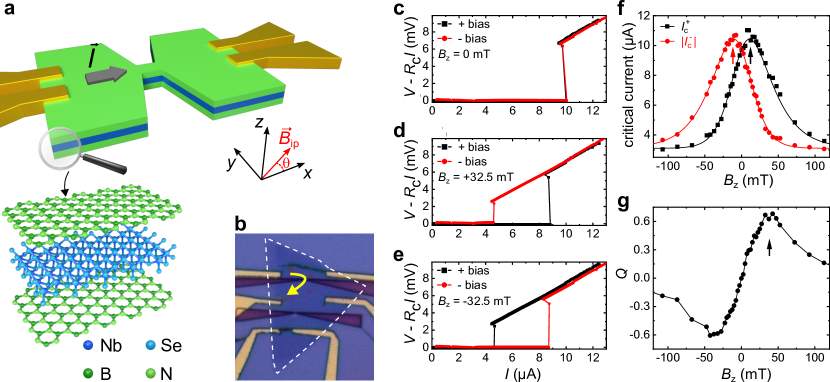
Our samples are fabricated using standard exfoliation methods for TMDs [15, 31, 32, 33]. A scheme of the typical device is depicted in Fig. 1a. The exfoliated NbSe2 crystals considered here are between 2 and 5 layers thick [32]. The flake thickness can be estimated with reasonable accuracy from the optical contrast of the crystal when stamped on standard SiO2/Si substrates. The parity of the layer number and the lattice orientation is determined, a posteriori, by second harmonic generation (SHG) measurements for all samples. NbSe2 crystals are fully encapsulated in hBN [33] and edge contacts are fabricated by electron beam lithography [13]. A 250 nm-long channel of 250 nm width is patterned by electron beam lithography and reactive ion etching. The etched parts appear as dark purple triangles in Fig. 1b. The purpose of the narrow channel is to have a well-defined direction of the current density in the constriction, direction indicated by in Fig. 1a. In what follows, the -direction is assumed to be that of the constriction axis (and thus that of the supercurrent) while the -direction is perpendicular to the sample plane.
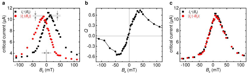
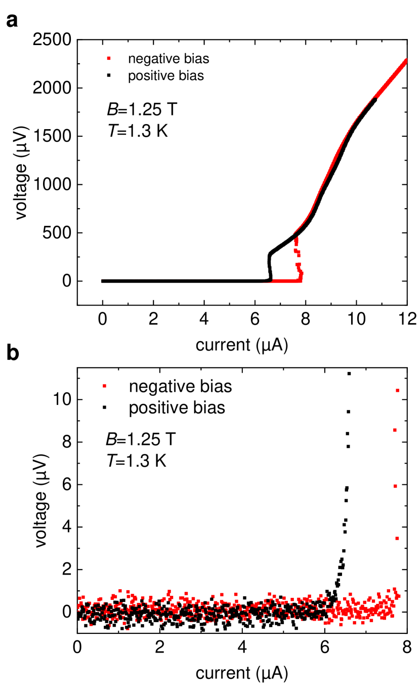
The main measurements of this work (sample F, see below) were performed in a dilution refrigerator equipped with a central superconducting coil controlling the in-plane component of the magnetic field. Additional coils provide a field perpendicular to the sample plane. A piezo-rotator allows for rotation of the sample around an axis normal to the sample plane. Additional measurements (samples B–E and G, see Supplementary Information) were performed in a 4He cryostat with a base temperature of 1.3 K, equipped with a single superconducting coil. Figures 1c-e introduce the supercurrent diode effect as measured in a NbSe2 constriction patterned on sample G. The graphs show three pairs of current-voltage characteristics (IVs) for applied out-of-plane magnetic fields of mT (c), mT (d) and mT (e). Importantly, all the IVs reported here always refer to the zero-to-finite (either positive or negative) bias sweep direction, in order to rule out heating effects. In the three graphs, the black (red) symbols refer to current density in the narrow channel oriented towards the positive (negative) direction. A strong supercurrent diode effect [17, 18] is evident from the comparison of the IVs: there is a marked difference in the critical current for the two supercurrent orientations, the sign of which change when the magnetic field is inverted. The complete field dependence of both (black) and (red) is plotted in Fig. 1f. The current range between and corresponds to the supercurrent diode regime, where current flows without dissipation only in one direction, which can be selected by changing the sign of the magnetic field [17]. As a figure of merit of the supercurrent diode effect one can take the supercurrent rectification efficiency [22], i.e. the difference between and normalized by their average, which is plotted in Fig. 1g versus . For moderate fields, increases almost linearly. The maximum magnitude of is above 60%, much larger than that (%) observed in Ref. [17]. Beyond a certain breakdown field mT the diode effect is gradually suppressed. This behavior is reminiscent of that observed in Rashba superconductors, see e.g. Fig. 2 in Ref. [17] and Fig. 3 in Ref. [18]. Theory models for Rashba superconductors [20, 23] predict a similar suppression, but the threshold field is expected to be of the order of the paramagnetic limit, i.e. much larger than the value observed in our and in literature experiments [17, 18]. Finally, we stress that the observations in Fig. 1f,g do not depend on the field sweep direction, as discussed in the Supplementary Information.
It is important to note that in our case the diode effect can be so strong that, for one of the two bias polarities, the critical current increases by increasing the magnetic field, reaching a maximum at nonzero field. This can be seen, e.g., in Fig. 1f for mT. The remarkable increase of the critical current (the origin of which certainly deserves further study) is important since it eliminates the possibility that the nonreciprocal supercurrent originates from nonreciprocal Joule heating due to, e.g., vortex motion through asymmetric barriers. In the latter case, the diode effect could result from a different rate of vortices traversing the constriction in the two transverse directions. Such different vortex creep rate would imply a different Joule dissipation, a different electron temperature and finally a different critical current for the two bias polarities. In contrast to our observations, the maximum critical current would then be always observed in absence of vortices, i.e., at . The irrelevance of vortices in our experiment is further discussed in the Supplementary Information.
We observed supercurrent rectification in other devices with the same nominal geometry. The supercurrent diode effect was clearly visible in all the samples where supercurrent could be measured, i.e., sample B, D, E, F, and G. Their layer number was determined by combining information from white-light optical and SHG microscopy [34, 35, 36, 37], as discussed in the Supplementary Information. We found a layer number for sample B, D and F, for sample E and for sample G. As for the Ising superconductivity, the supercurrent diode effect is not theoretically expected to occur in NbSe2 when is even, owing to the restored inversion symmetry. However, both Ising superconductivity (see Fig. 4 in Ref. [34]) and the supercurrent diode effect (this work) are experimentally observed for both even and odd . This fact is likely because of the relatively weak electronic coupling between the layers, which effectively renders NbSe2 a collection of monolayers [34].
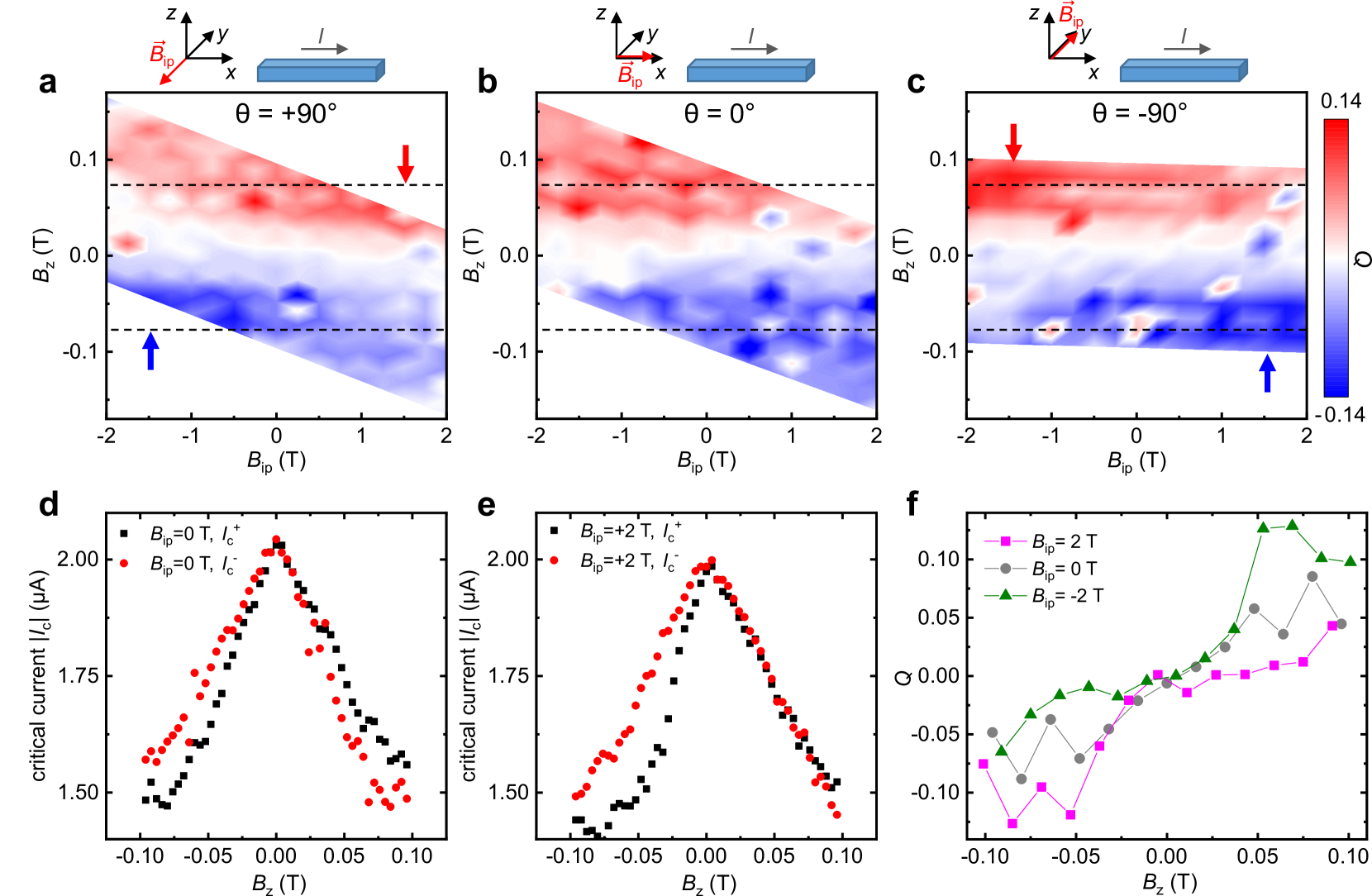
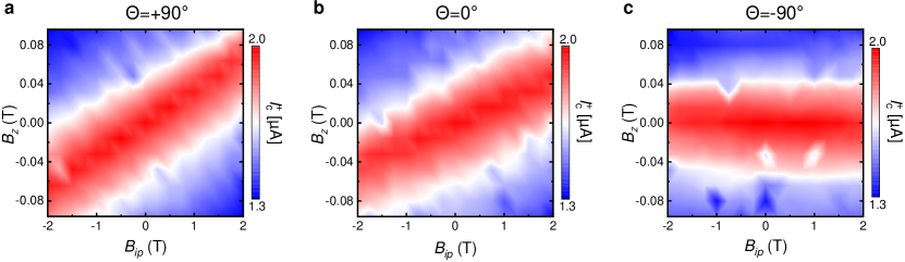
The experimental results shown in Fig. 1 clearly demonstrate that the out-of-plane field is required for the supercurrent diode effect in materials with valley-Zeeman spin-orbit. However, it is interesting to study whether the in-plane field also affects the rectification and, if it does, what the role of the components perpendicular and parallel to the current may be. For this reason, we measured one device, sample F, in a setup equipped with a piezo-rotator. This setup allows us to rotate the sample with respect to the main magnetic field , and therefore to control the angle between and supercurrent , as indicated in Fig. 1a. Additional coils, perpendicular to the main one, provide an independent control of the out-of-plane field . Figures 2a-c show the supercurrent rectification efficiency in sample F, plotted as a function of both the in-plane () and the out-of-plane () magnetic field, for (panel a, transverse to the supercurrent), for (panel b, parallel to the supercurrent), and for (panel c, antiparallel to that in panel a). Owing to sample misalignment, a large in-plane field produces a significant out-of-plane component. This misalignment can be quantified (and accounted for, as in Fig. 2a-c) by looking at the maximum of [or ], as discussed in the Supplementary Material. As a result of this offset adjustment, the data range in the plane appears as a rhomboid.
The most prominent feature in these measurements is the vertical gradient in the color plot, indicating that the rectification efficiency increases monotonically with and is zero when , at least within the experimental data scatter. We have therefore now established experimentally that, as predicted by theory [30], the supercurrent diode effect in TMDs is driven by the out-of-plane field only. In contrast, it is the in-plane field that drives the diode effect in Rashba superconductors. Moreover, unlike what is predicted for superconductors with pure valley-Zeeman SOI [30], we observe that the in-plane field does affect the supercurrent diode effect. More precisely, the in-plane field component perpendicular to the current breaks the (anti)symmetry of as a function of . If then , with no dependence on , see Fig. 2b. Instead, Fig. 2a,c prove that, for finite , , i.e., the diode effect becomes asymmetric in . This effect is apparent, e.g., in Fig. 2a: for the given field and current orientation, the diode effect is enhanced when and are both positive or negative (first and third quadrant of the graph, deep red and deep blue region, indicated by the arrows). On the other hand, it is suppressed when and have opposite signs (second and fourth quadrant, light red and light blue region). At fixed (dashed lines), inverting the sign of corresponds to a transition from enhanced to suppressed diode effect, i.e. from deep blue to light blue for the upper dashed line. Clearly, a sample rotation is equivalent to a sign change in , as it is evident by comparing Fig. 2a and Fig. 2c. It is important to remark that data in Fig. 2a-c are still (anti)symmetric upon simultaneous inversion of both and , i.e., .
To better visualize the impact of the in-plane field, it is instructive to look separately at and as a function of , both with and without in-plane field. The latter case is shown in Fig. 2d. Both and appear as asymmetric, -shaped functions. Their difference in slope for positive and negative produces a supercurrent diode effect increasing monotonically with . We note the similarity of Fig. 2d and Fig. 1f with the corresponding measurements on Rashba Josephson junctions, see Fig. 3e in Ref. [18]. As for Fig. 1g, the whole graph in Fig. 2d is symmetric if both the sign of and the direction of the supercurrent are changed simultaneously, i.e. for and . This symmetry is broken when an in-plane field is applied along the direction perpendicular to the supercurrent. In the case of . shown in Fig. 2e, the difference between the slope of and is reduced for and enhanced for , and vice versa for .
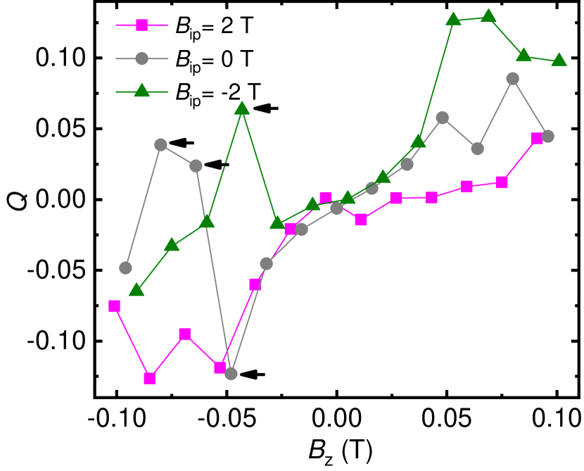
Figure 2f summarizes our main findings: the supercurrent rectification efficiency is plotted as a function of for and for T, 0 T and -2 T. The graph shows that the perturbation due to the in-plane field is evident only for sufficiently high out-of-plane field, i.e., mT. Above that threshold, for , the slope of versus increases strongly for T and decreases for T. The opposite is true for . We also note that at sufficiently large , above approximately 50 mT, the diode effect starts to be suppressed, so that at around mT the different curves in Fig. 2f merge again.
The key result of our observations is that the supercurrent diode effect in NbSe2 is controlled by the out-of-plane field, as predicted by theory for superconducting TMDs [30]. For there is no diode effect, independent of . On the other hand, if has a component perpendicular to the current, then the supercurrent diode effect becomes asymmetric in , i.e., it is enhanced for one out-of-plane field polarity and suppressed for the other. The role of the two polarities is swapped if both the sign of the supercurrent and the sign of are inverted. To the best of our knowledge, there are no predictions to date regarding a possible role of the in-plane field on the supercurrent diode effect in TMDs. On the contrary, for Rashba superconductors it is precisely the in-plane field that controls MCA and the diode effect [17, 18]. It is clear that further studies are needed to elucidate the role of the in-plane field in superconducting TMDs, which might be related to a possible Rashba-like component of the SOI [38, 39]. In NbSe2 such Rashba components can arise, e.g., due to ripples in the crystal [40] formed when stamping NbSe2 on hBN [33], or due to the substrate [41]. The existence of a weak Rashba SOI component in NbSe2 has, for example, been invoked to explain the apparent two-fold anisotropy of the magnetoresistance as a function of in-plane magnetic field [41]. The model proposed in Ref. [41] relies on the presence of -wave components in the pairing function, which might as well play a role in the anisotropy of the diode effect we observe here.
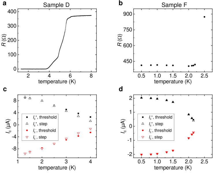
Next, we turn to the temperature dependence of . In the literature, theory predictions regarding the temperature dependence of the rectification efficiency are quite diverse. While some models predict a square-root-like dependence near the critical temperature [22], others suggest a more complex functionality [23]. Figure 3 shows the temperature dependence of the diode effect in samples D, F and G. In the graph we plot , obtained from in the linear regime of low field, where . We choose to display rather than because it represents a linear interpolation of and thus it averages over several data points, therefore showing a reduced scatter compared to for a given .
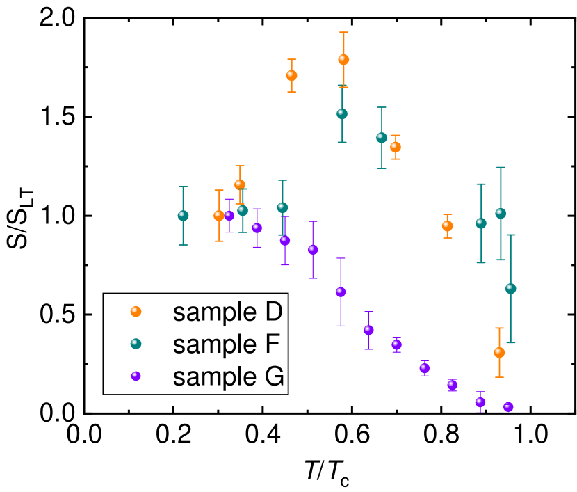
First of all, we observe that the supercurrent diode effect saturates at low temperature. This saturation is compatible with all theory models and similar to the results on Josephson junctions in Rashba superconductors [18]. This result is not obvious, since in the data in Ref. [17] the diode effect is visible only near and it is suppressed for both higher and lower temperatures. We note also that the temperature dependence of the diode effect in sample D and F is nonmonotonic, with a maximum reached near , where, instead, a kink is observed in sample G. A nonmonotonic temperature dependence of the rectification at finite field was also predicted by recent theory [23]. It is possible that the different behavior displayed by samples D, F and G is due to the fact that, in order to obtain a significant rectification, we need to apply a sufficiently strong field. Notice that theory in Ref. [23] predicts that the temperature dependence of the rectification is critically affected by a finite magnetic field.
A comment is in order about features which appear to be sample dependent. While the supercurrent diode effect was observed in every sample we measured (see Supplementary Information for further details), the maximum rectification efficiency is highly scattered among the samples, ranging from 6 to 60%. Also the supercurrent increase with is sample dependent, both in terms of relative increase and maximum supercurrent field . The supercurrent increase seems to be independent from the efficiency of the supercurrent rectification: the former is negligible in sample F, while in sample G no particular feature is observed in at . The nominal differences between the samples are the layer number and the orientation of with respect to the lattice. Both features can be determined by SHG microscopy performed after the transport measurements, as described in the Supplementary Information. We found that neither the layer number nor the supercurrent-to-lattice orientation are correlated with the magnitude of the rectification efficiency. On the other hand, lithography of narrow constrictions by reactive ion etching produces random disorder, in particular at the edges. This randomness, together with the still limited number of studied samples, does not allow us to conclusively assess the role of the lattice orientation. Further investigation is needed in order to elucidate how the supercurrent diode effect is influenced by the direction of current flow with respect to the crystal.
In conclusion, we have demonstrated a supercurrent diode effect in few-layer NbSe2. We show that the effect is controlled by the out-of-plane magnetic field, in contrast to what has been observed in Rashba superconductors, where the effect is driven by the in-plane field component directed perpendicular to the supercurrent. This field component nevertheless plays a role in NbSe2 devices as well, since it suppresses the diode effect for one out-of-plane field polarity and enhances it for the opposite one. Finally, the temperature dependence of the effect shows a saturation at low temperature, a maximum or a kink at around and a suppression near . TMD-based diodes can be crucial components in fully superconducting electronics. Their dissipation-free directional transport makes them suited for logic elements, ultrasensitive detectors, or signal demodulators, which can operate at low temperature with no energy loss. Being just a few atoms thick, their performance could conceivably be controlled electrically by gates, and modified by integrated them into complex van der Waals stacks in combination with other 2D materials.
During the review process we became aware of a related experimental work on supercurrent rectification in NbSe2/CrPS4 heterostructures [42], in NbSe2-based Josephson junctions [43], and on supercurrent rectification in magic-angle twisted bi- [44] and trilayer [45] graphene, and Nb-proximitized NiTe2 [46].
Methods
Sample preparation. NbSe2 crystals were purchased from HQ Graphene. hBN and NbSe2 crystals were exfoliated following two common techniques. One is the technique introduced in Ref. [31], where flakes are exfoliated on a polydimethylsiloxane (PDMS) film placed on a glass slide. Suitable crystals are then stamped onto the sample using a micromanipulator placed under a zoom-lens. The other technique is commonly used for the production of fully hBN-encapsulated graphene devices [15]. In this case, flakes are sequentially picked up by a thick PDMS film coated with polycarbonate (PC). The flake pick-up takes place at 120∘C, while the final release is triggered by melting the PC at 180∘C and by dissolving it in chloroform.
Both the fabrication of the contacts and the design of the constriction require an electron beam lithography step followed by reactive ion etching (RIE). For the RIE, a mixture of 6 sccm O2 and 40 sccm CHF3 is ignited into a plasma with 35 W r.f. forward power at a pressure of 35 mTorr. The RIE step etches through hBN and NbSe2 with an approximate etching rate of 0.45 nm/s. When electrodes have to be produced, immediately after the RIE step a 10 nm-thick layer of Ti and a 100 nm-thick film of Au are deposited. This procedure reflects the well-known recipe for edge contact fabrication in graphene. For sample G the RIE process was substituted by an Argon plasma etching process with 2 kV acceleration voltage and 20 mA plasma current at about mbar. The etching rate is in this case approximately 1 nm per minute.
Transport measurements. Measurements on sample F were performed in a dilution refrigerator with base temperature 30 mK. For electrical measurements we used DC lines with Cu-powder filters. Since one of the four electrodes stopped working after cool-down, we measured the device in a three-terminal configuration. The IV characteristics were thus obtained by subtracting the voltage , where 413 \textOmega is the contact resistance. In the IV curves, the resistive transition of the constriction at the critical current was clearly visible as a sharp step, except very close to the critical temperature and field.
The critical currents for data in Fig. 1 and Fig. 3 were determined from the IVs as the extrapolation on the current axis (abscissas) of the steep voltage increase at the resistive transition. In Fig. 2, owing to the larger amount of data, we used the alternative criterion µV, which is better suited for automatic routines. Nevertheless, the results shown here depend very weakly on the criterion for the critical current. We verified in all samples that the and data obtained with either criteria were nearly the same (see Supplementary Information for further details).
Measurements on the other samples (A–E,G) were performed in a 4He cryostat with only room temperature filtering (-filters). Except for sample G, the sample holder is positioned in such a way that the magnetic field produced by the superconducting coil is approximately in the plane of the sample surface. The misalignment (typically of the order of a few degrees) produces an out-of-plane field of tens of milliteslas per tesla of applied field. In sample G, instead, the sample is perpendicular to the main field, thus the field is applied exclusively out-of-plane.
Second harmonic generation measurements. Optical measurements of second harmonic generation (SHG) were always performed after transport measurements, in order to minimize the risk of photo-oxidation [33]. The co-polarized SHG intensity is measured as a function of the relative angle between laser polarization and crystal orientation [34, 35, 36, 37]. The monochromatic light source used was a pulsed Ti:sapphire laser (80 fs pulse duration, 80 MHz repetition rate, 1 mW power) at 800 nm. Using a microscope objective (40, numerical aperture of 0.6), the light was focused onto the NbSe2 samples placed in the vacuum chamber. The reflected SHG signal at 400 nm was collected with the same objective, filtered by a 680 nm short-pass filter, dispersed in a spectrometer (150 grooves/mm grating) and detected by a CCD camera. A linear polarizer was placed in front of the spectrometer to ensure acquisition of the signal polarized parallel to the laser polarization. A 50:50 non-polarizing beam splitter was used to separate the incident pathway from the signal detection pathway. In between the beam splitter and the objective, an achromatic half-wave plate was placed to change the relative angle between the crystal orientation and the laser polarization. The half-wave plate was rotated using a stepper motor. A 1200 grooves/mm grating was used as a reference sample. In the experiments, we used an exposure time of 1 s per data point.
Data and code availability
The data that support the findings of this study and the code needed to analyze the data are available from the corresponding author upon request.
Acknowledgments
Acknowledgements.
Acknowledgments. We thank Denis Kochan, Marco Aprili and Magdalena Marganska for useful discussions. The work was funded by the Deutsche Forschungsgemeinschaft (DFG, German Research Foundation) – Project-ID 314695032 – SFB 1277 (subprojects B03, B04, B08 and B11), and by the European Union’s Horizon 2020 research and innovation programme under grant agreements No 862660 QUANTUM E-LEAPS.Author contributions
N. Paradiso and C. S. conceived and designed the experiments. L. B., C. Bäuml, and N. Paulik fabricated the samples. L. B., L. F., C. Baumgartner and N.Paradiso, performed the transport experiments; L.B., J. M. L., K.-Q. L., and J. M. B. conceived and performed SHG measurements. K. W. and T. T. grew hBN crystals. All authors contributed to the preparation of manuscript.
Competing interests
The authors declare no competing interests.
Additional Information
Supplementary Materials: Additional measurements on sample G; Measurements on sample B; Summary description of other samples; Second harmonic generation measurements; Role of vortices; Field misalignment; Resistance and critical current versus temperature; Removal of outliers in Fig. 2f.
References
- Rikken et al. [2001] G. L. J. A. Rikken, J. Fölling, and P. Wyder, Electrical magnetochiral anisotropy, Phys. Rev. Lett. 87, 236602 (2001).
- Rikken and Wyder [2005] G. L. J. A. Rikken and P. Wyder, Magnetoelectric anisotropy in diffusive transport, Phys. Rev. Lett. 94, 016601 (2005).
- Ideue et al. [2017] T. Ideue, K. Hamamoto, S. Koshikawa, M. Ezawa, S. Shimizu, Y. Kaneko, Y. Tokura, N. Nagaosa, and Y. Iwasa, Bulk rectification effect in a polar semiconductor, Nature Physics 13, 578 (2017).
- Wakatsuki et al. [2017] R. Wakatsuki, Y. Saito, S. Hoshino, Y. M. Itahashi, T. Ideue, M. Ezawa, Y. Iwasa, and N. Nagaosa, Nonreciprocal charge transport in noncentrosymmetric superconductors, Science Advances 3, e1602390 (2017).
- Yasuda et al. [2019] K. Yasuda, H. Yasuda, T. Liang, R. Yoshimi, A. Tsukazaki, K. S. Takahashi, N. Nagaosa, M. Kawasaki, and Y. Tokura, Nonreciprocal charge transport at topological insulator/superconductor interface, Nature Communications 10, 2734 (2019).
- Itahashi et al. [2020] Y. M. Itahashi, T. Ideue, Y. Saito, S. Shimizu, T. Ouchi, T. Nojima, and Y. Iwasa, Nonreciprocal transport in gate-induced polar superconductor SrTiO3, Science Advances 6, eaay9120 (2020).
- Ideue et al. [2020] T. Ideue, S. Koshikawa, H. Namiki, T. Sasagawa, and Y. Iwasa, Giant nonreciprocal magnetotransport in bulk trigonal superconductor , Phys. Rev. Research 2, 042046 (2020).
- Zhang et al. [2020] E. Zhang, X. Xu, Y.-C. Zou, L. Ai, X. Dong, C. Huang, P. Leng, S. Liu, Y. Zhang, Z. Jia, X. Peng, M. Zhao, Y. Yang, Z. Li, H. Guo, S. J. Haigh, N. Nagaosa, J. Shen, and F. Xiu, Nonreciprocal superconducting NbSe2 antenna, Nature Communications 11, 5634 (2020).
- Lyu et al. [2021] Y.-Y. Lyu, J. Jiang, Y.-L. Wang, Z.-L. Xiao, S. Dong, Q.-H. Chen, M. V. Milošević, H. Wang, R. Divan, J. E. Pearson, P. Wu, F. M. Peeters, and W.-K. Kwok, Superconducting diode effect via conformal-mapped nanoholes, Nature Communications 12, 2703 (2021).
- Hoshino et al. [2018] S. Hoshino, R. Wakatsuki, K. Hamamoto, and N. Nagaosa, Nonreciprocal charge transport in two-dimensional noncentrosymmetric superconductors, Phys. Rev. B 98, 054510 (2018).
- Tokura and Nagaosa [2018] Y. Tokura and N. Nagaosa, Nonreciprocal responses from non-centrosymmetric quantum materials, Nature Communications 9, 3740 (2018).
- Strambini et al. [2021] E. Strambini, M. Spies, N. Ligato, S. Ilic, M. Rouco, C. G. Orellana, M. Ilyn, C. Rogero, F. S. Bergeret, J. S. Moodera, P. Virtanen, T. T. Heikkilä, and F. Giazotto, Rectification in a Eu-chalcogenide-based superconducting diode (2021), arXiv:2109.01061 [cond-mat.supr-con] .
- Bäuml et al. [2021] C. Bäuml, L. Bauriedl, M. Marganska, M. Grifoni, C. Strunk, and N. Paradiso, Supercurrent and Phase Slips in a Ballistic Carbon Nanotube Bundle Embedded into a van der Waals Heterostructure, Nano Letters 21, 8627 (2021).
- Huang et al. [2015] J.-W. Huang, C. Pan, S. Tran, B. Cheng, K. Watanabe, T. Taniguchi, C. N. Lau, and M. Bockrath, Superior current carrying capacity of boron nitride encapsulated carbon nanotubes with zero-dimensional contacts, Nano Letters 15, 6836 (2015).
- Wang et al. [2013] L. Wang, I. Meric, P. Y. Huang, Q. Gao, Y. Gao, H. Tran, T. Taniguchi, K. Watanabe, L. M. Campos, D. A. Muller, J. Guo, P. Kim, J. Hone, K. L. Shepard, and C. R. Dean, One-dimensional electrical contact to a two-dimensional material, Science 342, 614 (2013).
- Hu et al. [2007] J. Hu, C. Wu, and X. Dai, Proposed Design of a Josephson Diode, Phys. Rev. Lett. 99, 067004 (2007).
- Ando et al. [2020] F. Ando, Y. Miyasaka, T. Li, J. Ishizuka, T. Arakawa, Y. Shiota, T. Moriyama, Y. Yanase, and T. Ono, Observation of superconducting diode effect, Nature 584, 373 (2020).
- Baumgartner et al. [2022] C. Baumgartner, L. Fuchs, A. Costa, S. Reinhardt, S. Gronin, G. C. Gardner, T. Lindemann, M. J. Manfra, P. E. Faria Junior, D. Kochan, J. Fabian, N. Paradiso, and C. Strunk, Supercurrent rectification and magnetochiral effects in symmetric Josephson junctions, Nature Nanotechnology 17, 39 (2022).
- Note [1] Since the terminology has not settled yet in the literature, it is possible to find the term superconducting diode effect referred to resistance MCA, when this latter is enhanced by superconducting fluctuation near the critical temperature. Here, we refer exclusively to the (dissipationless) supercurrent diode effect.
- Yuan and Fu [2022] N. F. Q. Yuan and L. Fu, Supercurrent diode effect and finite-momentum superconductors, Proceedings of the National Academy of Sciences 119, e2119548119 (2022), https://www.pnas.org/doi/pdf/10.1073/pnas.2119548119 .
- Daido et al. [2022] A. Daido, Y. Ikeda, and Y. Yanase, Intrinsic superconducting diode effect, Phys. Rev. Lett. 128, 037001 (2022).
- He et al. [2022] J. J. He, Y. Tanaka, and N. Nagaosa, A phenomenological theory of superconductor diodes, New Journal of Physics (2022).
- Ilic and Bergeret [2022] S. Ilic and F. S. Bergeret, Theory of the supercurrent diode effect in Rashba superconductors with arbitrary disorder (2022), arXiv:2108.00209 [cond-mat.supr-con] .
- Halterman et al. [2022] K. Halterman, M. Alidoust, R. Smith, and S. Starr, Supercurrent diode effect, spin torques, and robust zero-energy peak in planar half-metallic trilayers, Phys. Rev. B 105, 104508 (2022).
- Davydova et al. [2022] M. Davydova, S. Prembabu, and L. Fu, Universal Josephson diode effect (2022), arXiv:2201.00831 [cond-mat.supr-con] .
- Zhai et al. [2022] B. Zhai, B. Li, Y. Wen, F. Wu, and J. He, Prediction of Ferroelectric Superconductors with Reversible Superconducting Diode Effect (2022), arXiv:2201.01775 [cond-mat.supr-con] .
- Scammell et al. [2021] H. D. Scammell, J. I. A. Li, and M. S. Scheurer, Theory of zero-field diode effect in twisted trilayer graphene (2021), arXiv:2112.09115 [cond-mat.mes-hall] .
- Zhang et al. [2021] Y. Zhang, Y. Gu, J. Hu, and K. Jiang, General theory of Josephson Diodes (2021), arXiv:2112.08901 [cond-mat.supr-con] .
- Zinkl et al. [2021] B. Zinkl, K. Hamamoto, and M. Sigrist, Symmetry conditions for the superconducting diode effect in chiral superconductors (2021), arXiv:2111.05340 [cond-mat.supr-con] .
- He et al. [2021] J. J. He, Y. Tanaka, and N. Nagaosa, A phenomenological theory of superconductor diodes in presence of magnetochiral anisotropy (2021), arXiv:2106.03575v1 [cond-mat.supr-con] .
- Castellanos-Gomez et al. [2014] A. Castellanos-Gomez, M. Buscema, R. Molenaar, V. Singh, L. Janssen, H. S. J. van der Zant, and G. A. Steele, Deterministic transfer of two-dimensional materials by all-dry viscoelastic stamping, 2D Materials 1, 011002 (2014).
- Paradiso et al. [2019] N. Paradiso, A.-T. Nguyen, K. E. Kloss, and C. Strunk, Phase slip lines in superconducting few-layer NbSe2 crystals, 2D Materials 6, 025039 (2019).
- Holler et al. [2019] J. Holler, L. Bauriedl, T. Korn, A. Seitz, F. Özyigit, M. Eichinger, C. Schüller, K. Watanabe, T. Taniguchi, C. Strunk, and N. Paradiso, Air tightness of hBN encapsulation and its impact on Raman spectroscopy of van der Waals materials, 2D Materials 7, 015012 (2019).
- Xi et al. [2015] X. Xi, Z. Wang, W. Zhao, J.-H. Park, K. T. Law, H. Berger, L. Forró, J. Shan, and K. F. Mak, Ising pairing in superconducting NbSe2 atomic layers, Nature Physics 12, 139 (2015).
- Malard et al. [2013] L. M. Malard, T. V. Alencar, A. P. M. Barboza, K. F. Mak, and A. M. de Paula, Observation of intense second harmonic generation from MoS2 atomic crystals, Phys. Rev. B 87, 201401 (2013).
- Li et al. [2013] Y. Li, Y. Rao, K. F. Mak, Y. You, S. Wang, C. R. Dean, and T. F. Heinz, Probing Symmetry Properties of Few-Layer MoS2 and h-BN by Optical Second-Harmonic Generation, Nano Letters 13, 3329 (2013).
- Lin et al. [2019] K.-Q. Lin, S. Bange, and J. M. Lupton, Quantum interference in second-harmonic generation from monolayer WSe2, Nature Physics 15, 242 (2019).
- Lu et al. [2015] J. M. Lu, O. Zheliuk, I. Leermakers, N. F. Q. Yuan, U. Zeitler, K. T. Law, and J. T. Ye, Evidence for two-dimensional Ising superconductivity in gated MoS2, Science 350, 1353 (2015), https://science.sciencemag.org/content/350/6266/1353.full.pdf .
- He et al. [2018] W.-Y. He, B. T. Zhou, J. J. He, N. F. Q. Yuan, T. Zhang, and K. T. Law, Magnetic field driven nodal topological superconductivity in monolayer transition metal dichalcogenides, Communications Physics 1, 40 (2018).
- Huertas-Hernando et al. [2006] D. Huertas-Hernando, F. Guinea, and A. Brataas, Spin-orbit coupling in curved graphene, fullerenes, nanotubes, and nanotube caps, Phys. Rev. B 74, 155426 (2006).
- Hamill et al. [2021] A. Hamill, B. Heischmidt, E. Sohn, D. Shaffer, K.-T. Tsai, X. Zhang, X. Xi, A. Suslov, H. Berger, L. Forró, F. J. Burnell, J. Shan, K. F. Mak, R. M. Fernandes, K. Wang, and V. S. Pribiag, Two-fold symmetric superconductivity in few-layer NbSe2, Nature Physics 17, 949 (2021).
- Shin et al. [2021] J. Shin, S. Son, J. Yun, G. Park, K. Zhang, Y. J. Shin, J.-G. Park, and D. Kim, Magnetic Proximity-Induced Superconducting Diode Effect and Infinite Magnetoresistance in van der Waals Heterostructure (2021), arXiv:2111.05627 [cond-mat.supr-con] .
- Wu et al. [2021] H. Wu, Y. Wang, P. K. Sivakumar, C. Pasco, S. S. P. Parkin, Y.-J. Zeng, T. McQueen, and M. N. Ali, Realization of the field-free Josephson diode (2021), arXiv:2103.15809 [cond-mat.supr-con] .
- Diez-Merida et al. [2021] J. Diez-Merida, A. Diez-Carlon, S. Y. Yang, Y. M. Xie, X. J. Gao, K. Watanabe, T. Taniguchi, X. Lu, K. T. Law, and D. K. Efetov, Magnetic Josephson Junctions and Superconducting Diodes in Magic Angle Twisted Bilayer Graphene (2021), arXiv:2110.01067 [cond-mat.supr-con] .
- Lin et al. [2021] J.-X. Lin, P. Siriviboon, H. D. Scammell, S. Liu, D. Rhodes, K. Watanabe, T. Taniguchi, J. Hone, M. S. Scheurer, and J. I. A. Li, Zero-field superconducting diode effect in twisted trilayer graphene (2021), arXiv:2112.07841 [cond-mat.mes-hall] .
- Pal et al. [2021] B. Pal, A. Chakraborty, P. K. Sivakumar, M. Davydova, A. K. Gopi, A. K. Pandeya, J. A. Krieger, Y. Zhang, M. Date, S. Ju, N. Yuan, N. B. M. Schröter, L. Fu, and S. S. P. Parkin, Josephson diode effect from Cooper pair momentum in a topological semimetal (2021), arXiv:2112.11285 [cond-mat.supr-con] .
- Note [2] A subtraction of 170 nA to corresponds to an addition of the same amount to .
Supplementary Information: Supercurrent diode effect and magnetochiral anisotropy in few-layer NbSe2
I Additional measurements on sample G
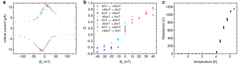
In this section we present additional experimental data from sample G. Figure S1a shows the raw data (namely, without subtraction of mT in and 170 nA in current) used to generate the plot in Fig. 1f of the main text. For each value of , ten IVs for positive bias and ten for negative bias where measured, whose critical current values are displayed in Fig. S1a. A certain distribution in the switching current is visible. Each data point in Fig.1f of the main text is obtained averaging over these points. Without the averaging, the scatter in would produce a larger scatter in , owing to the fact that this latter quantity is obtained from the difference between and .
Figure S1b shows measurements of the rectification efficiency as a function of for different -sweep directions. As for panel a, here we neither subtracted instrumental offsets, nor averaged the data. We notice that, within the data scatter, there is no apparent effect of the sweep direction.
Finally, Fig. S1c shows a curve as extracted from IV characteristics measured in a three-terminal configuration. Each data point is obtained by fitting the low bias part of the IV. The temperature independent value at low temperature ( \textOmega) is the source contact resistance, which is unavoidable in a three-terminal measurement. From the we deduce a K at the constriction. As for the other samples, this value is smaller than the typical for few-layer NbSe2 ( K), owing to the disorder introduced in the constriction by etching.
Offset removal in sample G. In Fig. S2a we show the same data as in Fig. 1f –namely, and for sample G– but, in this case, without removing the field offset (-2.5 mT) and the current offset (170 nA). The graph is nearly indistinguishable from that in Fig. 1f, indicating that the offset has only a minor impact. In particular, the current offset is about 1.5% of the maximum critical current. The resulting curve without offset removal is plotted in Fig. S2b. As a result of the offset, the curve appears slightly shifted (both horizontally and vertically) compared to Fig. 1g of the main text. Note that the offset is relatively small, comparable with the width of the switching current distribution discussed above: its effect becomes visible only in the averaged curves, as the one shown in Fig. 1g or Fig. S2b.
A subtraction of mT and nA from the nominal values of, respectively, and 222A subtraction of 170 nA to corresponds to an addition of the same amount to ., leads to a match of the and curves, that is required by time-reversal symmetry. The overlapping curves are shown Fig. S2c.
II Measurements on sample B
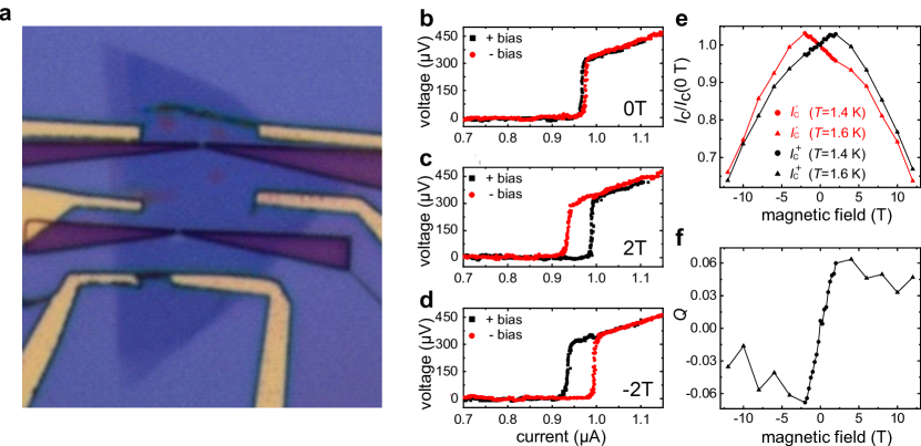
In this section we discuss measurements on sample B. This sample (as well as samples D, E discussed below) was measured in the 1K cryostat with the magnetic field oriented nominally in-plane (and perpendicular to the current direction within the constriction). Owing to a misalignment (of typically a couple of degrees) the field has also a small but decisive component out-of-plane which produces the supercurrent rectification. Clearly, to obtain a field of tens of mT, needs to be several teslas. On the other hand, owing to the characteristics of Ising superconductors, an in-plane field of few teslas has a little effect on the critical current.
Figure S3a shows a magnified version without contour lines of the micrograph in Fig. 1b of the main text. Figures S3b, c and d show IV-characteristics for an applied field of 0 T, 2 T and -2 T, respectively. This field magnitude corresponds roughly to the maximal rectification. Notice that the positive critical current for 2 T is clearly larger that that for 0 T: similar to sample G, sample B (as well as sample D and E, see below) shows an increase of the critical current with the field. for one polarity. Figure S3e shows the dependence of the positive (black) and negative (red) critical current on the magnetic field. Each curve contains points from two different measurements performed with different resolution and at slightly different temperature (high resolution: K, circles; low resolution: K, triangles). For better comparison, the critical current are displayed normalized to the zero field value. Finally Fig. S3f shows the field dependence of the rectification efficiency . Panels b-f are the corresponding ones of panels c-g in the Fig. 1 of the main text.
These measurements show that the qualitative behavior of sample B is similar to that of sample G. Owing to the unknown degree of misalignment, it is not possible to determine neither nor . However, since by experience the misalignment is of the order of a couple of degrees, we estimate to be in the range of several tens of mT, which is also in line with sample G and sample F.
III Summary description of the other samples
In this section we briefly describe other samples investigated within this project which have not yet been discussed so far, namely, samples A, C, D, E. The letter used to label the samples indicated the sequence of their fabrication (sample A first, sample G at last).
Sample A. In this sample, measured in 4-terminal configuration, the central constriction stayed normal all the way down to the base temperature of out 1K cryostat. This was likely caused by an unintentionally more aggressive reactive ion etching step, or by oxidation occurred after the lithographic fabrication of the constriction. Therefore, this sample shall not be further considered here.
Sample C. This sample has a different geometry (1 µm wide and 4 µm-long channel) and a different substrate (ceramic substrate for solid ion gating experiments) compared to all the others. It does not show a well-defined critical current: instead, it displays a series of phase slip lines, which some of the authors have studied in plain few-layer NbSe2 crystals [32]. Owing to the peculiarities of this sample, we shall not consider it further.
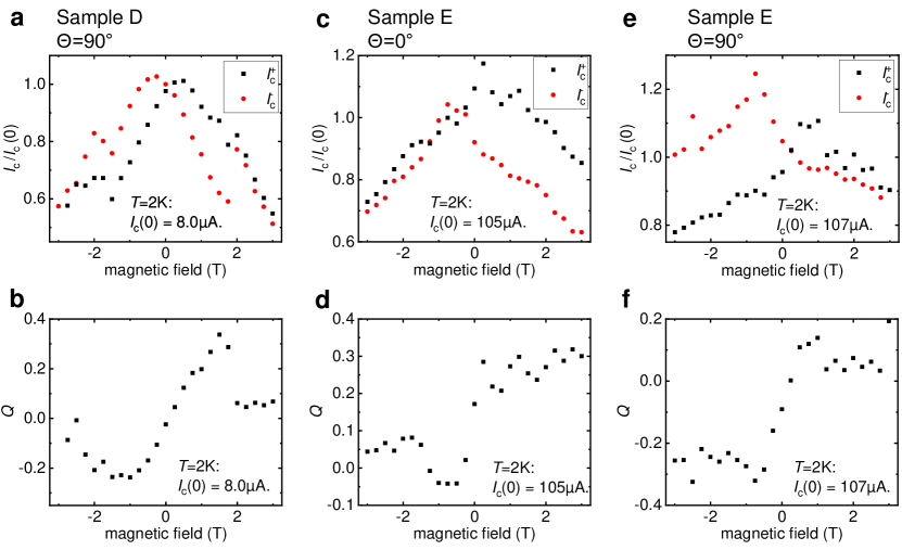
Sample D. This sample (nominally identical to A, B, E, F). The plot of the two critical currents and is similar to that in Fig. 1f of the main text. Similarly the plot of mirrors that in Fig. 1g. Critical current and supercurrent rectification efficiency measurements, reported in Fig. S4a, show a behavior similar to that observed in sample B, c.f. Fig. 1 of the main text. Also in this device the absolute value of the critical current increases with , reaching a maximum for T. This value is smaller than that for sample B (about 2 T), most likely owing to a larger field misalignment in sample D. This sample shows the second-largest rectification efficiency: for T, is as large as 33%, see Fig. S4b.
Sample E. The critical current of this device is very large. The value, well above 100 µA, is close to the critical current for an entire flake and it is clearly incompatible with a width of few hundreds nanometers which is that of the constriction. The most likely interpretation is that, due to some undetected problems during the reactive ion etching step, the etching depth did not exceed that of the top hBN layer, leaving the NbSe2 flake unaffected. As a consequence, the direction of the current is not well-defined as for the other samples. Despite this, we do observe a clear supercurrent diode effect, see Fig. S4c-f. From SHG measurements we deduce that the supercurrent direction within the constriction is nearly parallel (2∘ misalignment) to the armchair direction of the lattice, see next section.
We measured sample E in two cool-downs. In the first cool-down the applied field was mostly directed in-plane and parallel to the nominal constriction direction. In the second, the sample was rotated by so that the field was still mostly directed in-plane, but perpendicular to the nominal constriction direction. The lack of a well-defined constriction makes it difficult to disentangle the effect of the different field components. Possibly because of that, the and the plots appear asymmetric and distorted. It is important to remark that a supercurrent rectification is nevertheless observed, confirming the robustness of the diode effect in NbSe2.
Second harmonic generation measurements
To determine the armchair direction and layer number parity of the NbSe2 crystal, we measure the co-polarized SHG intensity as a function of relative angle between laser polarization and crystal orientation [34, 35, 36, 37] A Ti:sapphire laser (Spectra-Physics, Mai Tai XF, 80 MHz repetition rate, 80 fs pulse duration) at 800 nm was focused onto the NbSe2 samples placed in the vacuum chamber using a microscope objective (Olympus, LUCPLFLN 40) with numerical aperture of 0.6. The reflected SHG signal at 400 nm was collected with the same objective, filtered by a 680 nm short-pass filter (Semrock, FF01-680SP), dispersed in a spectrometer (Princeton Instruments, Acton SP2300) with a 150 grooves/mm grating, and detected by a CCD camera (Princeton Instruments, PIXIS 100). A linear polarizer was placed in front of the spectrometer to ensure acquisition of the signal parallel to the laser polarization. A 50:50 non-polarizing beam splitter was used to separate the incident path and signal detection path. An achromatic half-wave plate was placed between the beam splitter and the objective to change the relative angle between the crystal orientation and the laser polarization. The half-wave plate was rotated in 1∘ increments from 0∘ to 180∘ using a stepper motor, and the SHG intensity was recorded after each step. In general, a laser power of 1 mW and a single exposure time of 1 s were used for each measurement.
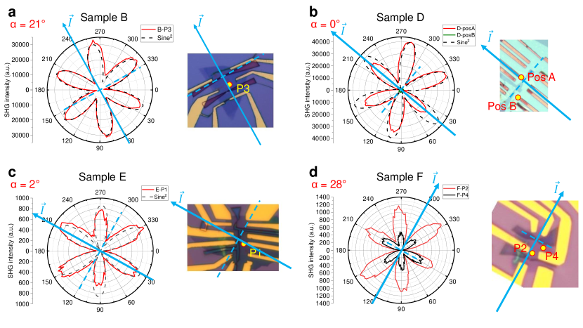
The polar plots in Fig. S5 show the typical six-fold symmetry pattern representing the three-fold symmetry of the transition metal dichalcogenide crystals. The maximum (minimum) intensity direction corresponds to the armchair (zigzag) direction of the crystal. The light blue arrow indicates the axis of the constriction, i.e., the direction of the supercurrent in the transport measurements. The arrow is reproduced on the optical micrograph on the right side of each panel: there, the perpendicular dashed line crosses the arrow exactly at the position where the constriction is located. The yellow dot indicates the position where the corresponding SHG measurement indicated in the graph was performed. In the figure, panel a, b, c, and d refer to sample B, D, E, and F, respectively. The angle between supercurrent and armchair direction is indicated in red on the top left of each panel. Only for sample G, the angle dependence is not reported: owing to its even number of layers, the SHG signal is very small, except at the very edges. This sample is also very homogeneous, therefore it does not feature terraces with odd which could allow us to perform an angle-resolved SHG measurements with a discernible signal. SHG measurements on this sample were nevertheless precious, since they confirmed its parity and demonstrated unambiguously that the supercurrent diode effect can be observed in crystals with both even and odd .
From the combination of optical microscopy and SHG measurements, we deduce that samples B, D, E, F, G consist of 3, 3, 5, 3, and 2 layers, respectively. In fact, optical microscope pictures do not make it always possible an univocal determination of the layer number: a typical optical micrograph is typically compatible with two consecutive values of .The parity determination provided by SHG eliminates the residual uncertainty in .
Concerning the direction of the supercurrent with respect to the underlying lattice, in sample D and in sample E the vector is almost perfectly aligned parallel to the armchair direction while in sample F is nearly parallel to the zig-zag direction. Finally, in sample B the orientation is intermediate, but closer to zig-zag.
We notice that the different magnitude of the supercurrent rectification factor among the samples does not seem to be correlated to the angle . The same applies to the other peculiar phenomenon observed in our experiment, namely, the increase of the critical current with the magnetic field. This effect produces an opposite horizontal shift of the -shaped and curves, see Fig. 1f of the main text and Fig. S4a-c here. The only sample where this effect is negligible (see Fig. 2d of the main text) is F, where is oriented approximately along the zig-zag direction. On the other hand, in sample B the effect is particularly pronounced, despite an angle relatively close to that for sample F.
IV The negligible role of vortices
In 2D Rashba superconductors the supercurrent diode effect is driven by in-plane magnetic field, as shown by experiments [17, 18] and predicted by theory [30]. Therefore, the presence of vortices can be, in principle, eliminated by careful compensation of the out-of-plane component. In contrast, in NbSe2 (and, more generally, in materials with valley-Zeeman spin-orbit interaction) it is precisely the out-of-plane field component that drives the supercurrent nonreciprocity, leading to the unavoidable presence of vortices. These might conceivably introduce spurious nonreciprocity, e.g. in the presence of an asymmetric barrier for entering/leaving the samples at the two edges of the constriction. However, the experimental evidence indicates that the presence of vortices does not play a significant role, owing to the following arguments.
-
1.
We do not observe a measurable dissipation in the IVs until we reach the critical current, and this remains true up to fields at least as large as . As an example, in Fig. S6 we show IV characteristics for sample D (where 4-terminal IV-characteristics are available). In this case, as described above, the field is applied mainly in-plane, with an important out-of-plane component (of the order of several tens of mT). Notice that there is no measurable foot within a voltage scale of 500 nV: at the critical current, the voltage emerges abruptly from the noise floor.
-
2.
If the diode effect were due to the asymmetry in the barrier for vortices entering/leaving the sample, the rectification would be extremely temperature dependent (following the temperature dependence of the penetration depth and thus of the vortex barrier) while approaching . Instead, the -dependence in sample D and F is even nonmonotonic, and in general it does not follow the typical -dependence of .
-
3.
If the vortex barrier played a significant role, one would expect a significant vortex trapping within the constriction, leading to hysteresis in the field sweep. Instead, as shown in Fig. S1b, the -sweep direction is irrelevant.
-
4.
If the diode effect were due to vortices, the in-plane field would not make the effect of asymmetric, as we observed in the experiments. A fortiori, the sign and orientation would be totally irrelevant, in contrast to results shown in Fig. 2 of the main text.
Magnetic field misalignment
As discussed in the main text, the alignment of the magnetic fields with respect to the sample surface is crucial for the interpretation of the data. In fact, the perturbing effect of is noticeable for fields of the order of teslas. On the other hand, a couple of degrees of field misalignment would produce a spurious out-of-plane field of the order of tens of milliteslas, more than sufficient to induce a sizeable diode effect.
The sample misalignment is due to two factors. First, the sample rotation axis might be not perfectly perpendicular to . Second, the sample surface might not be perfectly perpendicular to the rotation axis. Owing to both misalignment effects (each of the order of about 1 or 2 degrees) the angle between and the sample surface varies as a function of with -periodicity. As a consequence, measurements with at fixed will be affected by an offset proportional to , with constant of proportionality being a -periodic function of .
The determination of such an offset (and thus of the misalignment) can be easily achieved by measuring the critical current (either or ) as a function of the nominal and fields. For an Ising superconductor the application of a few teslas in-plane field has little impact on the critical current, while out-of-plane fields of even a few tens of milliteslas have a noticeable effect. Therefore, if we plot, as in Fig. S7, , the offset can be determined from the local maximum. For a given the maximum of must occur when the effective field is zero. This condition allows us to find, for that value of , the additional introduced by . We deduce that , where is the effective out-of-plane field (used in the main text, see Fig. 2a-c), is the nominally applied out-of-plane field, and is a coefficient such that , , and . Approximately, from measurements at other intermediate angles , we found that , with expressed in radians.
Resistance and critical current versus temperature
The graphs in Fig. S8a,b show the zero-bias resistance versus temperature for the constriction in sample D and F, respectively. Measurements on sample D were performed in 4-terminal, by combining an AC (lock-in amplifier) and a DC (digital-to-analog converter) voltage source, and by measuring the output current with a current amplifier and the voltage drop with a differential voltage amplifier. curves are obtained from the zero-bias differential resistance measured with the lock-in amplifier, while the critical current is obtained from the DC IVs. Measurements on sample F were performed in 3-terminal configuration (since one of the 4 contacts did not work), using only DC excitation. data are obtained from the low-bias slope of the IVs, upon subtraction of the constant contact resistance of 413 \textOmega. The temperature for which the resistance emerges from the noise floor of the deep superconducting state is 3.68 K in sample D and 2.2 K in sample F.
The graph in Fig. S8c shows the temperature dependence of the positive and negative critical current. We stress that, as throughout this work, the IVs from which we determine are always swept from zero bias to finite (either positive or negative) bias, in order to eliminate any possible heating effect. The full symbols in Fig. S8c refer to critical current values deduced from the threshold condition µeV. The empty symbols refer to critical current values deduced by extrapolating on the abscissas the steepest portion (corresponding to the critical bias step) of the IV characteristics. Note that, except for very close to , the critical current criterion is immaterial, since the IVs are discontinuous at . Close to , instead, the criterion tends to overestimate the critical current, since a finite resistance (and thus a finite voltage) might appear at low bias due to uncompensated vortices that get depinned, or to vortex-antivortex depairing close to the Berezinskii-Kosterlitz-Thouless (BKT) transition. On the other hand, the alternative criterion (extrapolation on the current axis of the steepest portion of the IV) is difficult to apply near since the step itself becomes highly smeared. In Fig. S8c we plotted only points where the IVs display a sufficiently well-defined voltage step. From the convergence of the open symbols on the -axis ( condition), we deduce a critical temperature K. This value is slightly higher than that ( K) corresponding to the emergence of a finite zero-bias resistance. This discrepancy is probably due to the aforementioned dissipative processes occurring below the mean field .
Figure S8d is the analogue of Fig. S8c for sample F. In this case from the convergence of the empty symbols onto the -axis we deduce K, which is very close to the temperature value ( K) where a finite resistance emerges.
In the main text, we have used as values the ones deduced from the convergence of the curves onto the temperature axis, i.e., the criterion. Therefore we assigned K for sample D and K for sample F.
Outliers in Fig. 2f of the main text
In Fig. 2f of the main text four points (three data points, , and mT for the curve T; one data point mT for the curve T) were strong outliers. To reduce scatter we substituted the outliers with the corresponding points measured for the adjacent value (i.e., T instead of 0 T, T instead of -2 T). Figure S9 shows the original data. The outliers are indicated by arrows. Outliers are also visible in the color plots in Fig. 2a-c. They might may conceivably originate from temperature instabilities during the measurements.