Spatially-resolved electronic structure of stripe domains in IrTe2 through electronic structure microscopy
Abstract
Abstract:
Phase separation in the nanometer- to micrometer-scale is characteristic for correlated materials, for example, high temperature superconductors, colossal magnetoresistance manganites, Mott insulators, etc. Resolving the electronic structure with spatially-resolved information is critical for revealing the fundamental physics of such inhomogeneous systems yet this is challenging experimentally. Here by using nanometer- and micrometer-spot angle-resolved photoemission spectroscopies (NanoARPES and MicroARPES), we reveal the spatially-resolved electronic structure in the stripe phase of IrTe2. Each separated domain shows two-fold symmetric electronic structure with the mirror axis aligned along 3 equivalent directions, and 61 replicas are clearly identified. Moreover, such electronic structure inhomogeneity disappears across the stripe phase transition, suggesting that electronic phase with broken symmetry induced by the 61 modulation is directly related to the stripe phase transition of IrTe2. Our work demonstrates the capability of NanoARPES and MicroARPES in elucidating the fundamental physics of phase-separated materials.
State Key Laboratory of Low-Dimensional Quantum Physics and Department of Physics, Tsinghua University, Beijing 100084, P. R. China
Synchrotron SOLEIL, Université Paris-Saclay, L’Orme des Merisiers, Saint Aubin-BP 48, 91192 Gif-sur-Yvette Cedex, France
Madrid Institute of Materials Science (ICMM), Spanish Scientific Research Council (CSIC), Cantoblanco, E-28049 Madrid, Spain
Department of Mechanical Engineering and Tsinghua-Foxconn Nanotechnology Research Center, Tsinghua University, Beijing 100084, P. R. China
Frontier Science Center for Quantum Information, Beijing 100084, P. R. China
∗ Email: syzhou@mail.tsinghua.edu.cn
Introduction
By focusing the beam size down to a few m or even 100 nm scale by a Fresnel zone plate[1, 2, 3] (for synchrotron light source) or a lens[4] (for laser source), nanometer- and micrometer-spot angle-resolved photoemission spectroscopies (NanoARPES[1, 2, 3] and MicroARPES[4], Fig. 1a) provide two important advantages over conventional ARPES which has a typical beam size of 50-100 m. Firstly, it allows to measure the electronic structure of small samples, which has been demonstrated in atomically thin flakes[5, 6, 7] or samples with mixed crystal orientations[8, 9]. Secondly and more importantly, for phase-separated materials which consist of multiple domains with distinct electronic structures[10, 11, 12, 13, 14], the newly added spatial-resolving capability provides new opportunities to reveal the intrinsic electronic structure of individual domain and the evolution of the phase separation across the phase transition. Such information cannot be obtained by conventional ARPES, which is, however, indispensable for understanding the fundamental physics of phase-separated materials. Recently, NanoARPES and MicroARPES have been applied to probe the electronic structure of individual domain in CeSb[15] and Fe-based superconductors[16, 17, 18, 19] by utilizing the spectroscopic capability of ARPES. Combining the advantages of both microscopic and spectroscopic capabilities of NanoARPES and MicroARPES will allow for direct visualization of separated domains with spatially-resolved information and the evolution of domains across the phase transition, thereby further elucidating the complex physics of phase-separated materials.
IrTe2 exhibits an intriguing stripe phase with separated domains at low temperature, where the electronic structure in the stripe phase has remained elusive. Upon cooling, it undergoes a first order phase transition from trigonal (1T with Pm1 symmetry, see Fig. 1b) to triclinic structure (P) around 280 K, accompanied by complex stripe phase[20] with periods of (3n+2)1(3n+2) (n = 1,2,3,…) in the bulk[20, 21] and (3n+2)1 on the surface[22, 23]. Recent scanning tunnelling microscopy and ARPES study on strained IrTe2 shows 61 phase can be stabilized by strain[24]. Suppressing the stripe phase by doping or intercalation[20, 25] leads to emergence of superconductivity. To understand the stripe phase, different scenarios have been proposed including Fermi surface nesting[20] or saddle point[26] induced charge density wave, crystal field effect[27], dimerization[28, 29], local bonding[30, 31] and lattice deformation[32]. Obtaining the electronic structure of the stripe phase is critical for disentangling the puzzling physics. Despite extensive investigations, previous ARPES measurements on IrTe2[33, 26, 32, 34, 35, 36, 37, 38] have been obtained by averaging over different domains, and the intrinsic electronic structure of each individual stripe domain and its temperature evolution across the phase transition remain elusive.
Here, by using NanoARPES and MicroARPES, we resolve the separated domains and electronic structure of individual stripe domain in IrTe2. Each separated domain shows two-fold symmetric electronic structure with the mirror axis aligned along 3 equivalent directions, and 61 reconstructions are clearly identified both in the Fermi surface map and the dispersion, suggesting 61 stripe phase. Moreover, such electronic structure inhomogeneity disappears across the stripe phase transition, suggesting that electronic phase with broken symmetry induced by the 61 modulation is directly related to the stripe phase transition of IrTe2. Our work demonstrates the power of NanoARPES and MicroARPES in elucidating the physics across the phase transition.
Results and discussion
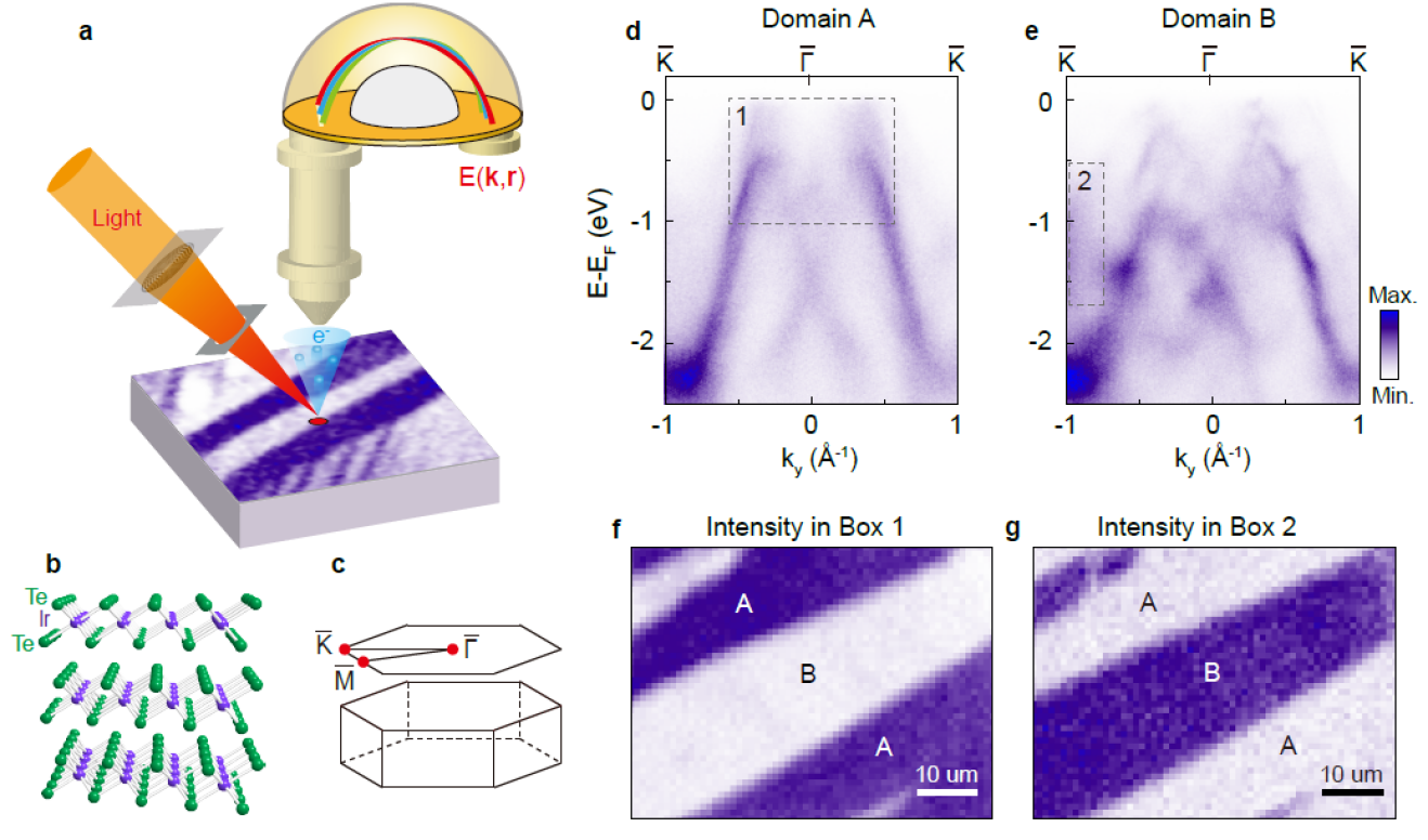
Spatially-resolved electronic structures of different domains. Figure 1d,e shows two representative NanoARPES spectra measured along the - direction (Fig. 1c) of IrTe2 at 80 K from two domains A and B, and they are strikingly different. While the dispersion in domain A is relatively simple with strong intensity at energies from -2.5 to -0.5 eV, the dispersion in domain B shows weak intensity starting from -1 eV to the Fermi energy (EF) with many weaker bands near EF. In addition, compared to domain A, there is an additional band near the point (marked by box 2 in Fig. 1e). Spatially-resolved intensity maps (Fig. 1f,g) integrated over box 1 and 2 allow to directly visualize the spatial distribution of these two types of domains with size of a few to tens of micrometers. Since the sample is a high quality single crystal with a well-defined crystal orientation, the observation of separated domains with different electronic structures therefore suggests that IrTe2 is an intrinsically inhomogeneous material.
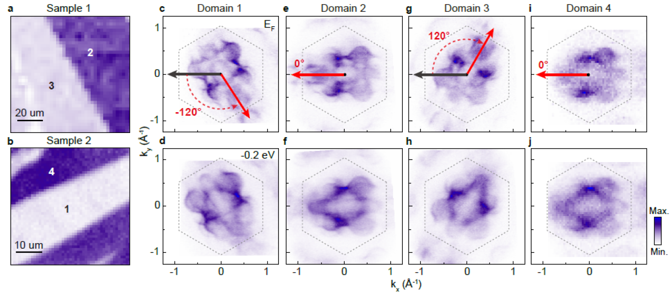
To further investigate the electronic structure of these separated domains, we map out the full three-dimensional electronic dispersions for each domain. Figure 2a,b shows the spatially-resolved intensity maps measured on two representative samples where separated domains are clearly observed. Figure 2c-j shows the intensity maps at and -0.2 eV from four different domains. All these intensity maps clearly reveal the two-fold symmetry of the electronic structure with the symmetry axis aligned along three equivalent - directions at angles of 0∘, 120∘ and -120∘ (indicated by red solid arrows), which is in sharp contrast to previous ARPES measurements[33, 26, 32, 34, 35, 36, 37, 38] where spatial averaging gives rise to apparently three-fold symmetric electronic structure. Therefore, the strikingly different dispersions in Fig. 1 originate from different orientations of the mirror symmetry axes. Here, the observation of two-fold symmetric electronic structure in a three-fold symmetric crystal confirms the broken symmetry in the stripe phase, and the space- and momentum-resolving capability allows to reveal the intrinsic electronic structure of each individual domain.
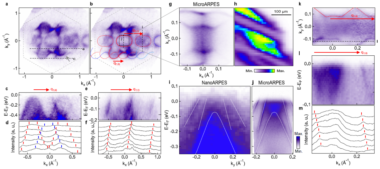
With the capability to resolve the electronic structure of each individual domain, we can now investigate the intrinsic electronic structure and the nature of the stripe phase. The two-fold symmetric Fermi surface map (Fig. 3a) shows replica oval pockets around the point translated by a scattering wave vectors of 1/3 a∗ (Fig. 3b) where a∗ is the reciprocal lattice vector. More replica pockets can be distinguished away from the point translated by 1/6 a∗ which fit well with the extra weak bands as indicated by the gray arrow in Fig. 3a. The replica pockets are also identified in the dispersion images shown in Fig. 3c, e and can be observed more clearly in the momentum distribution curves (MDCs) shown in Fig. 3d, f. We note that fine features are observed inside the replica oval pocket translated by 1/3 a∗ from . These features are absent in the oval pocket at , yet their existence can be confirmed by zooming in the intensity map (Fig. 3g) near point using our home-built MicroARPES system with a laser source at 6.2 eV (compared to 100 eV used in synchrotron based NanoARPES measurements) with better energy and momentum resolution. A comparison of NanoARPES and MicroARPES dispersion images (Fig. 3i,j) measured along two equivalent momentum directions displaced by 1/3 a∗ as indicated by dotted lines in Fig. 3b shows a good agreement yet with sharper peaks for MicroARPES, further confirming the electronic reconstruction with a scattering vector of 1/3 a∗. The spatially-resolved intensity map measured by MicroARPES in Fig. 3h also shows separated domains with domain size up to hundred micrometers. The electronic reconstruction of 1/6 a∗ is also observed in the zoom-in Fermi surface (Fig. 3k, also see Supplementary Figure 8 and Supplementary Note 4), dispersion image (Fig. 3l) and corresponding MDCs (Fig. 3m) in the MicroARPES data. We have performed fine spatial scan on 5 different samples using MicroARPES where the domain size varies, however, the dispersions of individual domain remain the same (see Supplementary Figure 1, 2, 7 and Supplementary Note 1), suggesting that the measured dispersions are independent of the domain size. By combining NanoARPES and MicroARPES measurements, we reveal the electronic reconstructions of 1/6 and 1/3 a∗, which suggests that the two-fold symmetric electronic structure is likely associated with the 61 reconstruction in the stripe phase. We note that in principle 51 or 81 would also be compatible with the two-fold symmetric Fermi surface, however signatures of 51 or 81 replicas have not been resolved experimentally, suggesting that those domains do not have significant contribution to the dispersions.
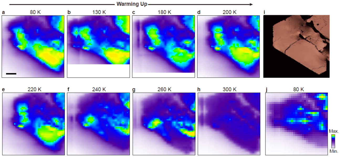
Temperature evolution of the spatially-resolved intensity map. To confirm that such spatial inhomogeneity is directly related to the stripe phase transition, we perform temperature-dependent MicroARPES measurement. Figure 4a-h shows spatially-resolved intensity maps measured at temperatures from 80 K to 300 K. Separated domains on the order of tens to hundreds of micrometers with different intensity contrast are clearly observed below the stripe transition temperature. Remarkably, above the stripe phase transition temperature, the spatial intensity map becomes much more homogeneous at 300 K (Fig. 4h) similar to its optical image. After cooling back to 80 K, the spatial inhomogeneity appears again but with different distribution, suggesting that its distribution is related to history (Fig. 4j). The observation of the stripe domains and its disappearance at high temperature provides direct evidence that the inhomogeneous electronic structure is an intrinsic property of the low temperature stripe phase.
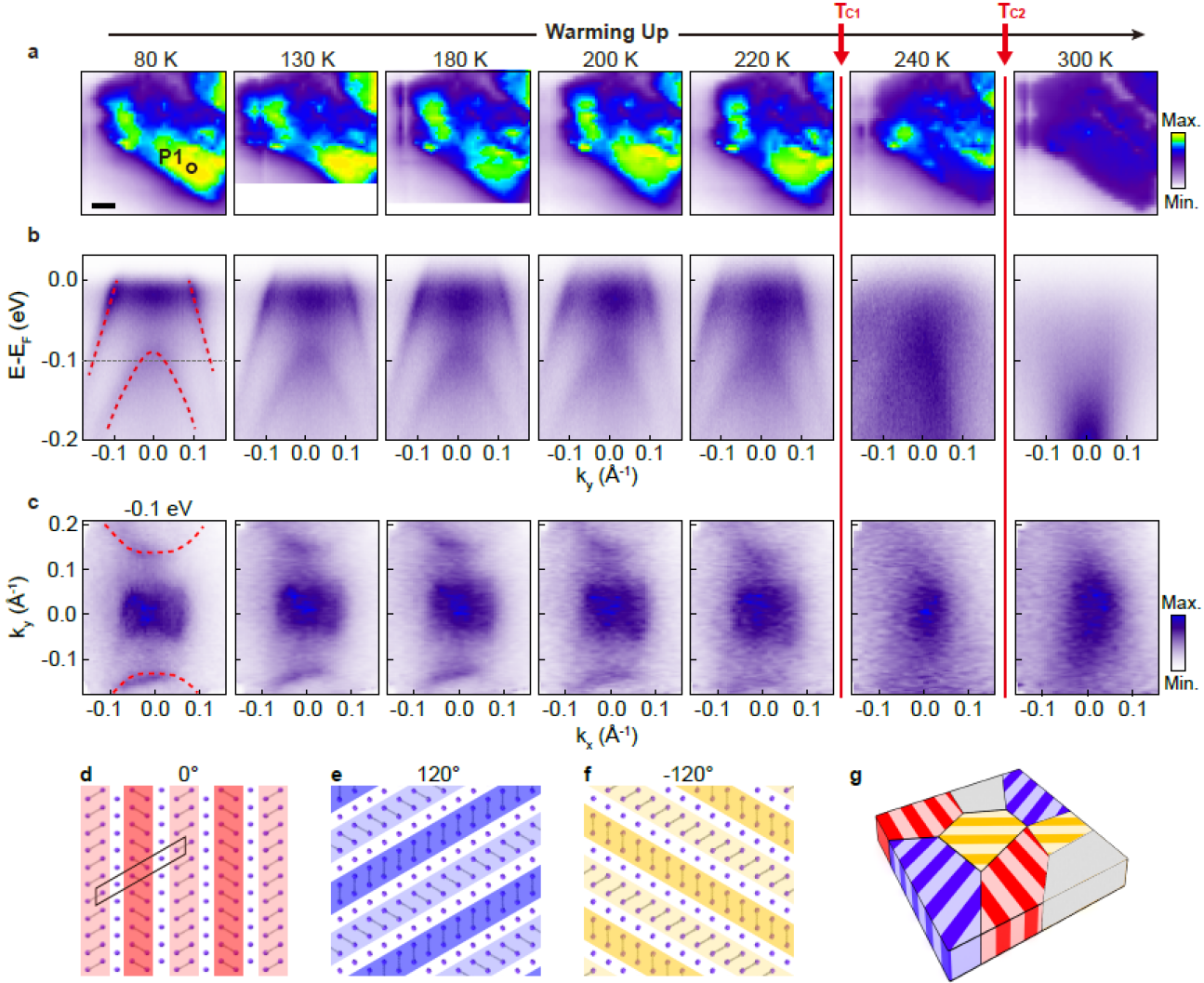
Figure 5a-c further shows the temperature evolution of the dispersion and intensity map measured in a single domain. Sharp dispersions near the point are observed at low temperature and they disappear at 240 K and above. As was discussed above, the sharp dispersions are associated with the 61 reconstruction, and their disappearance indicates a phase transition from 61 to other reconstructions at Tc1[23]. Further warming leads to another transition at Tc2 near 300 K, which corresponds to the transition to 11 phase. Similar evolution of the Fermi surface maps and dispersions is also observed for other domains but with a rotation angle of 120∘ (see Supplementary Figure 3 and Supplementary Note 2). In addition, broad dispersions and Fermi surface maps are also observed in some other locations (see Supplementary Figure 4), suggesting that there are also other regions in addition to the 61 stripe, which is possibly caused by the small percentage of coexisting 81 domain as revealed in LEED measurement shown in Supplementary Figure 5. Therefore, temperature dependent MicroARPES measurements show that the spatial inhomogeneity is directly related to the different orientations of the stripe phases, and there is a coexistence of both 61 stripe domains with different stripe orientations (Fig. 5d-g) and other mixed domains (gray area in Fig. 5g) as schematically shown in Fig. 5g.
Conclusion
In summary, the energy-, momentum- and space-resolving capability of NanoARPES and MicroARPES allows to visualize the separated domains and reveal the intrinsic and inhomogeneous electronic structure in the stripe phase of IrTe2. Replica bands with 1/6 a∗ wave vector (or 61 modulation) are identified in the dispersion which resembles the 61 reconstruction of the high temperature electronic state (see Supplementary Figure 6 and Supplementary Note 3). We note that the period of the phase is strongly related to the Ir-Ir dimer concentration, and different dimer concentration leads to complex (3n+2)1 stripe period. At the highest dimer concentration[39, 21], this corresponds to the 61 electronic ground state (Fig. 5d-f). Here by directly revealing the electronic structure of each individual domain using NanoARPES and MicroARPES, we show that the 61 stripe phase is indeed the electronic ground state and the 61 modulation is directly related to the stripe phase transition of IrTe2. Our work resolves the puzzle in the electronic structure of the stripe phase of IrTe2, and we envision that the application of NanoARPES and MicroARPES to other phase-separated systems can yield important information on the intrinsic underlying physics.
0.1 Sample growth.
High quality IrTe2 single crystal was grown by self-flux method. Ir pellet (99.95%, Alfa Aesar) and Te ingot (99.99%, Alfa Aesar) in an atomic ratio of 5:95 were mixed together and sealed in an evacuated silica ampoule. The mixture was heated up to 900 ∘C first and kept for several hours, then to 1150 ∘C and kept for two days, finally cooled down to 920 ∘C in several hours with a low rate. Liquid Te was separated from IrTe2 single crystal by centrifugation.
0.2 ARPES measurement.
MicroARPES measurements have been performed in the home laboratory at Tsinghua University with fourth harmonic generation light source. The photon energy is set to 6.2 eV with -polarization. The energy resolution was set to 15 meV. The beam size is 15 m. The sample was measured in a working vacuum at greater than Torr. Surface sensitive NanoARPES measurements were performed at the beamline ANTARES of the synchrotron SOLEIL[3] at France with a beam size of 150 nm. The photon energy is 100 eV. The energy and angular resolution were set to 25 meV and 0.1 deg, respectively.
References
References
- [1] Dudin, P. et al. Angle-resolved photoemission spectroscopy and imaging with a submicrometre probe at the SPECTROMICROSCOPY-3.2L beamline of Elettra. J. Synchrotron Radiat. 17, 445–450 (2010).
- [2] Bostwick, A., Rotenberg, E., Avila, J. & Asensio, M. C. Zooming in on electronic structure: NanoARPES at SOLEIL and ALS. Synchrotron Radiat. News 25, 19–25 (2012).
- [3] Avila, J. & Asensio, M. C. First NanoARPES user facility available at SOLEIL: An innovative and powerful tool for studying advanced materials. Synchrotron Radiat. News 27, 24–30 (2014).
- [4] Schwirr, E. et al. Applications for ultimate spatial resolution in LASER based -ARPES: a FeSe case study. AIP Conf. Proc. 2054, 040017 (2019).
- [5] Wilson, N. R. et al. Determination of band offsets, hybridization, and exciton binding in 2D semiconductor heterostructures. Sci. Adv. 3, 1601832 (2017).
- [6] Zhang, H. et al. Resolving deep quantum-well states in atomically thin 2H-MoTe2 flakes by nanospot angle-resolved photoemission spectroscopy. Nano Lett. 18, 4664–4668 (2018).
- [7] Katoch, J. et al. Giant spin-splitting and gap renormalization driven by trions in single-layer WS2/h-BN heterostructures. Nat. Phys. 14, 355–359 (2018).
- [8] Bao, C. et al. Stacking-dependent electronic structure of trilayer graphene resolved by nanospot angle-resolved photoemission spectroscopy. Nano Lett. 17, 1564–1568 (2017).
- [9] Yao, W. et al. Quasicrystalline 30∘ twisted bilayer graphene as an incommensurate superlattice with strong interlayer coupling. Proc. Natl. Acad. Sci. 115, 6928–6933 (2018).
- [10] Uehara, M., Mori, S., Chen, C. & Cheong, S. Percolate phase separation underlies colossal magnetoresistance in mixed-valence manganites. Nature 399, 560 (1999).
- [11] Pan, S. H. et al. Microscopic electronic inhomogeneity in the high-Tc superconductor Bi2Sr2CaCu2O8+x. Nature 413, 282 (2001).
- [12] Dagotto, E. Complexity in strongly correlated electronic systems. Science 309, 257 (2005).
- [13] Qazilbash, M. et al. Mott transition in VO2 revealed by infrared spectroscopy and nano-imaging. Science 318, 1750 (2007).
- [14] Lai, K. et al. Mesoscopic percolating resistance network in a strained manganite thin film. Science 329, 190 (2010).
- [15] Kuroda, K. et al. Devil’s staircase transition of the electronic structures in CeSb. Nat. Commun. 11, 2888 (2020).
- [16] Watson, M. D. et al. Probing the reconstructed Fermi surface of antiferromagnetic BaFe2As2 in one domain. npj Quantum Materials 4, 36 (2019).
- [17] Ma, J. et al. Spatial nematic fluctuation in BaFe2(As1-xPx)2 revealed by spatially and angle-resolved photoemission spectroscopy. Phys. Rev. B 101, 094515 (2020).
- [18] Rhodes, L. C., Watson, M. D., Haghighirad, A. A., Evtushinsky, D. V. & Kim, T. K. Revealing the single electron pocket of FeSe in a single orthorhombic domain. Phys. Rev. B 101, 235128 (2020).
- [19] Chen, Y. et al. Visualization of the electronic phase separation in superconducting KxFe2-ySe2. Nano Research 14, 823–828 (2021).
- [20] Yang, J. J. et al. Charge-orbital density wave and superconductivity in the strong spin-orbit coupled IrTe2:Pd. Phys. Rev. Lett. 108, 116402 (2012).
- [21] Pascut, G. L. et al. Series of alternating states with unpolarized and spin-polarized bands in dimerized IrTe2. Phys. Rev. B 90, 195122 (2014).
- [22] Hsu, P.-J. et al. Hysteretic melting transition of a soliton lattice in a commensurate charge modulation. Phys. Rev. Lett. 111, 266401 (2013).
- [23] Chen, C. et al. Surface phases of the transition-metal dichalcogenide IrTe2. Phys. Rev. B 95, 094118 (2017).
- [24] Nicholson, C. W. et al. Uniaxial strain-induced phase transition in the 2D topological semimetal IrTe2. Commun. Mater. 2, 1–8 (2021).
- [25] Kamitani, M. et al. Superconductivity in CuxIrTe2 driven by interlayer hybridization. Phys. Rev. B 87, 180501 (2013).
- [26] Qian, T. et al. Structural phase transition associated with van Hove singularity in 5d transition metal compound IrTe2. New J. Phys. 16, 123038 (2014).
- [27] Ootsuki, D. et al. Orbital degeneracy and peierls instability in the triangular-lattice superconductor Ir1-xPtxTe2. Phys. Rev. B 86, 014519 (2012).
- [28] Pascut, G. L. et al. Dimerization-induced cross-layer quasi-two-dimensionality in metallic IrTe2. Phys. Rev. Lett. 112, 086402 (2014).
- [29] Eom, M. J. et al. Dimerization-induced Fermi-surface reconstruction in IrTe2. Phys. Rev. Lett. 113, 266406 (2014).
- [30] Cao, H. et al. Origin of the phase transition in IrTe2: Structural modulation and local bonding instability. Phys. Rev. B 88, 115122 (2013).
- [31] Saleh, G. & Artyukhin, S. First-principles theory of phase transitions in IrTe2. J. Phys. Chem. Lett. 11, 2127–2132 (2020).
- [32] Kim, K. et al. Origin of first-order-type electronic and structural transitions in IrTe2. Phys. Rev. Lett. 114, 136401 (2015).
- [33] Ootsuki, D. et al. Electronic structure reconstruction by orbital symmetry breaking in IrTe2. J. Phys. Soc. Jpn. 82, 093704 (2013).
- [34] Lee, H. et al. Electronic reconstruction on dimerized IrTe2. Europhys. Lett. 120, 47003 (2017).
- [35] Ootsuki, D. et al. A novel one-dimensional electronic state at IrTe2 surface. J. Phys. Soc. Jpn. 86, 123704 (2017).
- [36] Interplay between spin-orbit interaction and stripe-type charge-orbital order of IrTe2. J. Phys. Chem. Solids 270–274 (2018).
- [37] Monney, C. et al. Robustness of the charge-ordered phases in IrTe2 against photoexcitation. Phys. Rev. B 97, 2 (2018).
- [38] Rumo, M. et al. Examining the surface phase diagram of IrTe2 with photoemission. Phys. Rev. B 101, 235120 (2020).
- [39] Li, Q. et al. Bond competition and phase evolution on the IrTe2 surface. Nat. Commun. 5, 5358 (2014).
This work is supported by National Natural Science Foundation of China (Grants No. 11725418 and 11427903), the National Key R&D Program of China (Grants No. 2020YFA0308800, 2016YFA0301004), Tsinghua University Initiative Scientific Research Program and Tohoku-Tsinghua Collaborative Research Fund, and Beijing Advanced Innovation Center for Future Chip (ICFC). We acknowledge SOLEIL for provision of synchrotron radiation facilities.
Shuyun Z. conceived the research project. C.B. and Hongyun Z. performed the NanoARPES measurements and analyzed the data. C.B., Q.L., Shaohua Z., L.L., K.D. and W.Y. performed the Laser-based Micro-ARPES measurements and analyzed the data. Haoxiong Z., K.Z. and Y.W. grew and characterized the samples. C.C., J.A. and M.C.A. provided support for the NanoARPES experiments. C.B. and Shuyun Z. wrote the manuscript, and all authors commented on the manuscript.
All other authors declare no competing interests.
The data that supports the findings of this study are available within the article.