Distinguishing thermal from non-thermal (“hot”) carriers in illuminated molecular junctions
Abstract
The search for the signature of non-thermal (so-called “hot”) electrons in illuminated plasmonic nanostructures requires detailed understanding of the non-equilibrium electron distribution under illumination, as well as a careful design of the experimental system employed to distinguish non-thermal electrons from thermal ones. Here, we provide a theory for using plasmonic molecular junctions to achieve this goal. We show how non-thermal electrons can be measured directly and separately from the unavoidable thermal response, and discuss the relevance of our theory to recent experiments.
Keywords:plasmonics, electron non-equilibrium, molecular junctions, hot carriers.
keywords:
plasmonics, electron non-equilibrium, molecular junctions, thermo-electric effects, thermometryChem-BGU]Department of Chemistry, Ben-Gurion University of the Negev, Be’er Sheva, Israel 8410501 SECE-BGU] School of Electrical and Computer Engineering, Ben-Gurion University of the Negev, Be’er Sheva, Israel 8410501 SECE-BGU] School of Electrical and Computer Engineering, Ben-Gurion University of the Negev, Be’er Sheva, Israel 8410501
1 Introduction
When a plasmonic nanostructure is continuously illuminated, two things happen simultaneously. First, the system unavoidably heats up, and second, non-thermal (so-called “hot”) carriers (NTCs) are being generated. The latter effect leads to an electron (and hole) distribution that deviates from the equilibrium (Fermi-Dirac) distribution 1, 2. There has been growing interest in understanding the interplay between these two processes; non-thermal carriers were suggested to be beneficial for various applications, including, notably, photodetection 3, 4, 5, 6, 7 and plasmon-driven chemistry 8, 9, 10, 11, 12, 13, 14. However, the latter application is very sensitive to the temperature of the system. Thus, distinguishing between NTCs and thermal effects is crucial for understanding how (and if at all) NTCs can be used to, e.g., catalyse certain reactions.
Various indirect ways were proposed to determine the non-thermal electron population. These include primarily the study of the ultrafast dynamics of the metal permittivity via transient reflectivity measurements 15, 16, 17, 18, 19 and of the photoemission 20, 21, 22, 23 following illumination by an ultrashort pulse. Under such conditions, a relatively large number of high energy non-thermal electrons are being generated, but it is not clear when and how to separate those from mere heating. In contrast, under continuous wave illumination, it is clear that the information about heating is characterized by Fermi-like distribution of carriers close to the Fermi level, whereas the NTCs reside further away from the Fermi level in nearly-flat “shoulders”, see Ref. [ 2, 24]. However, the practical separation between thermal and non-thermal carriers is very challenging, because the number of the high excess-energy non-thermal electrons is many orders of magnitude smaller compared to the number of thermal (i.e., low excess energy) carriers. Thus, the various attempts made to directly quantify the contributions of these two types of charge carriers (e.g., to chemical reaction rates in the context of plasmon-assisted photocatalysis), frequently fail 25, 26, 27, 28, because the control thermocatalysis (light off) experiments must reproduce exactly the temperature profile of the photocatalysis (light on) experiments 26, 14, a task which is nearly impossible (although progress has been made in this direction 29, 30, 31, 32, 33, 34).
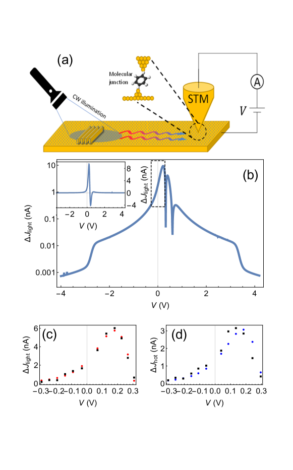
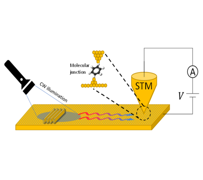
In an attempt to circumvent this problem, Reddy, Wang and co-authors 35 (referred to as RW20 hereafter) recently suggested measuring directly the NTC distribution by coupling a plasmonic Au film to a molecular junction (schematically described in Fig. 1(a), adapted from RW20). By measuring the I-V curves through the molecular junction (MJ) under illumination and in the dark, these authors assess directly the effect of illumination on the electronic distribution in the illuminated Au electrode.
The theoretical foundations to describe the non-thermal electron distribution as well as the current through such a plasmonic MJ were laid in Ref. [ 1]. We recently extended the first part of the model of Ref. [ 1] to provide a complete model of the electron non-equilibrium under CW illumination 2, 24. Here, we extend the second part of the theory of Ref. [ 1], namely, transport through a MJ coupled to two electrodes, by combining the standard Landauer theory of transport through MJs 36, 37 and the analytic form for the electron non-equilibrium distribution of an illuminated metal 24, and suggest a scheme that can be used to measure the non-thermal electron distribution in the presence of strong heating and even large thermal gradients (i.e., regardless of the temperature distribution). Using this formulation we shed new light on the experimental results of Reddy, Wang et al., 35 demonstrating that it is possible that they indeed were able to distinguish (probably for the first time) non-thermal electrons from thermal ones, but not in the way interpreted in the original manuscript. Specifically, we show that the signature of non-thermal electrons is weak in some of the key measurements of RW20, which can be explained alternatively via a purely thermal model. However, we point out that the signature of non-thermal electrons is dominant in some other experiments that have been performed by the authors of RW20.
2 Results and Discussion
2.1 General Theory
Current through a molecular junction is typically described by the Landauer formula 36, 37, which relates the total current to the electronic transmission function and the electrodes’ electron distribution functions, ; here, is the electron charge, is Planck’s constant, and represent the electron distribution of the top/bottom electrodes (representing the STM tip and the Au slab, respectively); see Fig. 1(a). At equilibrium, , where is the thermal (Fermi-Dirac) distribution, the (electron) temperature, the chemical potential and the Boltzmann constant. The transmission function is typically described by a Lorentzian, , where is the energy of the frontier molecular orbital and is the level broadening (this is the so-called wideband approximation 36, 37). Notably, the Landauer formula implicitly assumes that the electron and temperature distributions on the electrodes is uniform. We point that this approach ignores the direct effect of illumination on the electrons in the molecule, which is justified because the illumination is off-resonance with the molecular HOMO-LUMO gap (and also with which may affect transport 38), and hence the effect is negligible. It also disregards electron interactions in the molecule, which may shift the resonance position, but steal lead to Lorentzian-like transmission 39, 40. These approximations were also used in, e.g., RW20.
With equal distributions on the two electrodes, the current vanishes. As bias voltage is applied, the chemical potentials shift such that and current flows through the junction(we hereafter treat voltage in units of electron-volt). Current can also be driven by a temperature difference (i.e., setting ), generating a thermo-electric effect 36, 37, 41.
For the current to give an indication on the non-thermal electron distribution, it needs to be generated using optical illumination in an asymmetric manner, such that electric field felt by the electrodes is substantially different, and as a result, 42, 43, 44, 45. The MJ geometry enables this naturally; indeed, electromagnetic and thermal simulations of a generic MJ geometry reveals significant differences in the local fields and temperature across the MJ, see SI section 3.1. To evaluate this effect, we follow Ref. [ 24] (specifically its Appendix A), where it was shown that under continuous illumination (i.e., by monochromatic light at frequency ), the electron distribution in a Drude metal is (to an excellent approximation)111We point that while other formulations of the electron non-equilibrium exist, their limitations (see discussion in Ref. [ 2, 24]) make them unsuitable for separating thermal from non-thermal effects.
| (1) |
where measures the population of non-thermal carriers, or more precisely the deviation of the distribution function from its equilibrium form, and is given by
| (2) |
Here, is the local electric field intensity and is a constant that depends on the (imaginary part of the) metal permittivity at the laser frequency , and electron density but not on (see SI Section 3.1)222Note that the expression for in the original derivation 24 had a small typo; it was corrected in an errata, and noted in Ref. [ 46]. ; is the collision rate, for which we adopt the Fermi liquid theory, being the scattering constant 47. The importance of high energy non-thermal (i.e., “hot”) carriers, via the change in the distribution due to hot carriers, can be simply quantified by evaluating , namely, the value of at an energy 1eV above the Fermi energy, which captures the deviation from a thermal distribution at high energies. Notably, the solution for the non-equilibrium distribution (1) is also obtained under the assumption of uniform (or averaged) field.
Evaluating the current through an asymmetrically illuminated MJ can now be easily done by setting (assuming that the bottom electrode is grounded35) and plugging these distributions into the Landauer formula for the current. To isolate the contribution of illumination, we follow the authors of Ref. [ 35] who subtracted from the current under illumination the current in the dark (both as a function of voltage). In this case, the contribution to the current from illumination is simply
| (3) |
Eq. (3) implies that the current is determined by the electric field and electron temperature rise induced by the illumination at both electrodes. We use numerical simulations to evaluate these quantities, and then we evaluate for various molecular and illumination conditions. We show below that, depending on the properties of the molecular system, has a dominant feature coming from either the temperature difference or the NTC contribution.
2.2 Results - nearly-resonant molecules
We start with addressing a ”nearly-resonant” molecule, i.e., a molecule for which the orbital energy is close to the electrodes’ Fermi level (generally, it can represent either the HOMO or LUMO levels in the molecule, depending on the molecular moiety). In Fig. 1(b), we plot (the log of the absolute value of) as a function of voltage for a molecular junction, taking relevant parameters for a typical MJ, eV and meV; the relatively small value of makes this molecule ”nearly-resonant” (with respect to the electrodes’ Fermi level). We take (which corresponds to the value we calculate from microscopic consideration, see SI Section 3) and eV (corresponding to nm wavelength); note that the chosen wavelength is sufficiently longer than the eV threshold for interband transitions 48, thus, validating the use of the analytic solution for Drude metals (Eqs. (1)-(2)). We further set K, and assume that the illuminated slab under the STM tip is heated by K (i.e., K). These parameters are close to those presented in RW20. We also assume (as in RW20) that the STM tip itself is not heated ().
In this case, since the non-thermal part of the distribution is negligible for realistic values of voltage bias ( in RW20), the contribution of the light to the current is given by35
| (4) | |||||
is plotted in Fig. 1(b), showing two prominent features. The first is that the strongest current occurs at low voltages, close to ; this is due to a thermal effect (coming from the heating of the slab under illumination), centered a width around the orbital resonance 41, 36. Specifically, the absolute value of has only a minor effect on the results of Fig. 1(b); it is the difference between the temperature of the bottom electrode upon illumination and its temperature in the dark which is responsible for the large changes near . In that regard, this thermal feature is not a “thermo-electric” effect, meaning that increasing the tip temperature (and hence, modifying the temperature difference between the electrodes) has a negligible effect on the current difference . The second feature is the onset of non-thermal electron “shoulders” 2 in , which extend into the high-V regime, where the thermal effect becomes small. Fig. 1(b) shows ”spikes” or dips in . These are simply changes of sign in which appear as spikes in the log-plot, and do not have any special physical meaning (see the inset to Fig. 1(b), which shows the same data on a linear scale).
Armed with these insights from Fig. 1(b) (mainly that at low bias voltages thermal effects are dominant for a nearly-resonant molecule), we used Eq. (3) to fit the measured values of of RW20 for their L1 molecule (a charge-transfer complex of quaterthiophene (T4) and tetracyanoethylene (TCNE) with terminal thiophenes containing gold-binding methyl sulfides; data extracted from the supplementary material (Fig. S16A in RW20)). We use data from two sets of measurements in RW20, using Au slabs with thicknesses and nm. We set as free parameters both the molecular parameters and and the local temperature in the Au slab segment directly under the STM tip, , where is the ambient temperature and is the excess temperature of the slab above ambient; we again assume that the top electrode remains unheated. We simultaneously fit both data sets with the same and , leaving only to vary between experiments.
In Fig. 1(c)-(d) we plot the experimental data and a best fit to Eq. (3) (black squares) with common parameters eV and eV, with K and K for the and nm slabs (red and blue circles, respectively). These fits indicate that a thermal origin for the experimental results is plausible. Importantly, associating with a thermal effect naturally explains the two energy scales appearing in the data (the position of the peak and the linewidth ), which, in contrast, cannot be associated with any feature of NTCs (e.g., in Eq. (2)). Note that while these same results were interpreted in RW20 as the “hot” carrier contribution, no direct fit between theory and experiment was presented in RW20. In fact, while it is customary to refer to “hot” electrons in the energy range close to the Fermi energy, the match of our Drude-based analysis to the measured data confirms that in this energy range, there is predominantly only thermal electrons, i.e., electrons that are characterized by a Fermi-Dirac distribution (with a temperature potentially higher than ambient) whereas the number of true non-thermal electrons is much smaller (proportional to )333An exception to this statement may occur in the presence of interband transitions, and due to the minute deviation of the distribution from equilibrium discussed in Fig. 2(a) of Ref. [ 2]. . However, we also note that the signature of true non-thermal electrons would have been visible for higher voltages, via the pronounced lower current peak at energies above , compare the solid and dashed lines in Fig. 1(b); unfortunately, this regime was not accessible experimentally.
Finally, we note that our best fit parameters mentioned above yield a rather small temperature rise in the Au slab below the STM tip (K). In SI Section 3.2, we explain why these values, as well as the negligible heating assumed in both RW20 and our analysis, are likely to match numerical thermal simulations of the experimental system for the (hard-to-simulate) several micron-wide STM tip, as indeed were supposedly used in RW20. Moreover, we show in SI section 2 that the data of RW20 can be fitted even to different slab temperatures.
Despite the compelling match of the fit and our simulations and analysis, a few words of caution are in order. Our fits seem to be somewhat inconsistent with some of the data presented in RW20. For instance, the fitted values for and are different from those obtained in RW20 (although the estimates in RW20 are also inconsistent with some of their data, see SI Section 1), but are consistent with earlier measurements of a similar junction 49. Our results also show a discrepancy with the control experiments performed in RW20, where current in the dark was measured at increased temperatures (RW20, Fig. S12), and showed essentially no sign of being temperature sensitive. On the other hand, these control experiments are inconsistent with the formalism and parameters used within RW20. Indeed, plugging the RW20 parameters into a calculation of the current reveals a strong dependence on temperature (for the same parameters of RW20 Fig. S12), yet no such temperature dependence was measured; see SI Section 3.3 for further discussion.
2.3 Off-resonance molecule
The difficulty in distinguishing the thermo-electric and non-thermal electron contributions to stems from the two following points: (i) one cannot measure directly the sample temperature under the STM tip, and (ii) because of the relatively small (the nearly-resonant nature of the molecule), and the fact that thermal current response is limited to a width around the molecular orbital 41, 36, the thermal effect is most important for low (hence realistic) voltages, i.e., for molecular resonances around the Fermi level.
Overcoming the first point is very challenging. However, overcoming the second point is actually quite easy. In a molecular junction where the molecular orbital energy is far from the Fermi level but in resonance with the illumination energy (i.e., ), low voltage measurements of will only show the non-thermal part of the distribution. This is because, as is evident from Eq. (1) and the Landauer formula, the non-thermal features extend to a distance from the molecular resonance, and will thus be prominent at low voltages.
In this case, since the thermal contribution is negligible, the contribution of the illumination to the current is given by
| (5) |
where are derived (using Eq. (2)) from the local field on the bottom/top electrodes. Note that in Eq. (5) only electrons are considered, i.e., the correction to the distribution corresponding to holes () is disregarded, since holes will shift the distributions further away from the resonance and will not contribute to .
In Fig. 2 we plot (the log of) as a function of bias voltage (as in Fig. 1(b)) for the case of eV, at resonance with (all other parameters are the same as for L1, solid line), for . It is clear that now the thermal feature only appears at high (hence, inaccessible) voltages, while at low voltages, the non-thermal electron “shoulder” provides the prominent contribution to the current. For comparison, the dashed line shows for (i.e., no non-thermal electrons), demonstrating the orders-of-magnitude larger contribution of non-thermal electrons at low voltages. Importantly, there are also qualitative differences with respect to a nearly-resonant molecule like L1, most prominent is the fact that does not change sign, a feature which can be easily recognized experimentally (indeed, see below).
A somewhat similar experiment was, in fact, conducted in RW20, using a MJ with a 1,4-benzenediisonitrile molecule (dubbed L2 in RW20). This molecule has a LUMO level which is far from the Fermi level, eV 50, and thus is somewhat similar to the situation described above. In the SI to RW20 (Fig. S18), the authors plot vs. the bias voltage. We use these data to fit Eq. (3), and find that for this molecular energy indeed the thermal contribution is negligible for that range of voltages, and that the data can be fitted very well (within the experimental error) with the contribution coming solely from the non-thermal part of the distribution. This is shown in the inset to Fig. 2 where the experimental data (blue points) and the theoretical points (black squares) are shown. The molecular parameters eV and eV are taken from Ref. [ 50], and the only fit parameters are and .
To reduce the number of fit parameters further, we have conducted numerical simulations of the electric field under the experimental conditions (see SI Section 3.1). These simulations show that the field in the tip is actually larger than the field in the slab by a factor of , due to the plasmonic enhancement around the tip.
In the inset to Fig. 2 we plot the experimental data of RW20 (blue points, along with the experimental error bars), and the theoretical as a function of bias voltage, where (and keeping ) is found to provide the best fit value. This fit between data and theory provides further experimental corroboration to Eq. (3), providing what is, to the best of our knowledge, the first direct measurement of the steady-state non-thermal contribution to the electron distribution. These values for match the calculated values for the electric field (see SI Section 3.1) and are in good correlation with reported “hot” electron efficiencies in plasmon-assisted photocatalysis experiments 29, 51, 32.
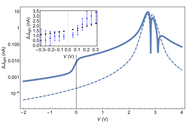
However, somewhat unintuitively, the experimental data of the L2 molecule in RW20 can also be explained by simple heating. Indeed, by setting the ’s to be zero and assuming K we obtain a fit essentially similar to that shown in the inset of Fig. 2; note that this is not a contradiction with Fig. 2, because the energy of molecule L2 obtained from the fit is much lower (i.e., not as far from resonance) compared with the value used for the illustration of Fig. 2; in that respect, the experiment in RW20 involves an intermediate case, whereby the molecular energy is only partially off-resonance. One is thus facing a situation where both NTCs and thermal effects can reproduce the experimental data.
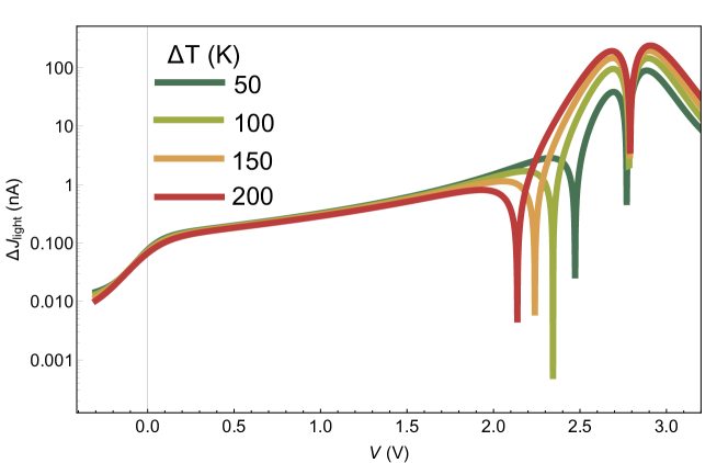
Fortunately, unlike the situation in plasmon-assisted photocatalysis experiments (e.g., Ref. [ 25]), the MJ setup offers a simple way to further discriminate between the two effects, by simply measuring (for the off-resonance molecule) as a function of the ambient temperature. The reason is that while the thermal contribution would be strongly influenced by the temperature, the NTCs would not (see Eq. (1) and Ref. [ 24]. In order to demonstrate this, in Fig. 3, we plot as a function of bias voltage for K, and as can be seen, the low-voltage NTC contribution to is essentially unchanged. Another way to overcome the situation is to choose a molecular junction which has frontier orbitals which are even further away from the Fermi level of the electrodes, such as Au-benzenedithiol-Au junctions, where the HOMO level is eV away form the Fermi level 52. Under such circumstances, the thermal effect is expected to contribute only a tiny fraction of the NTC contribution to .
3 Summary
In conclusion, we have shown that our analytical prediction of the electron distribution under continuous wave illumination can be used to interpret recent experiments (RW20). This sheds new light on these experiments, and demonstrates that they seem to measure directly the NTC contribution to the distribution function, however, surprisingly, not as they originally interpreted their data. We suggest further experiments that can be analyzed within our theory, and the necessary improvements to state-of-the-art theories for the electron non-equilibrium distribution and current through a MJ, thus, providing a direct route to solving one of the outstanding questions in plasmonic systems, namely, the form of the electron distribution under continuous illumination. Finally, the methodology presented here can be used for as a starting point for a theoretical treatment of other experiments where nano-scale transport is coupled to plasmonic effects 53, 54, 55, 56, 54, 57.
Supplementary Information includes additional transport calculation details, fit parameters and thermal calculations. This material is available free of charge via the internet at http://pubs.acs.org.
References
- Kornbluth et al. 2013 Kornbluth, M.; Nitzan, A.; Seidman, T. Light-induced electronic non-equilibrium in plasmonic particles. J. Chem. Phys. 2013, 138, 174707
- Dubi and Sivan 2019 Dubi, Y.; Sivan, Y. “Hot electrons” in Metallic Nanostructures - Non-Thermal Carriers or Heating? Light: Sci. Appl. 2019, 8, 89
- Goykhman et al. 2011 Goykhman, I.; Desiatov, B.; Khurgin, J.; Shappir, J.; Levy, U. Locally Oxidized Silicon Surface-Plasmon Schottky Detector for Telecom Regime. Nano Lett. 2011, 11, 2219–2224
- Goykhman et al. 2012 Goykhman, I.; Desiatov, B.; Khurgin, J.; Shappir, J.; Levy, U. Waveguide based compact silicon Schottky photodetector with enhanced responsivity in the telecom spectral band. Opt. Exp. 2012, 20, 28594
- Mubeen et al. 2013 Mubeen, S.; Lee, J.; Singh, N.; Kraemer, S.; Stucky, G. D.; Moskovits, M. An autonomous photosynthetic device in which all charge carriers derive from surface plasmons. Nat. Nanotech. 2013, 8, 247–251
- Li and Valentine 2016 Li, W.; Valentine, J. Harvesting the Loss: Surface Plasmon-Based Hot Electron Photodetection. Nanophotonics 2016, 6, 177–191
- Tagliabue et al. 2018 Tagliabue, G.; Jermyn, A. S.; Sundararaman, R.; Welch, A. J.; DuChene, J. S.; Pala, R.; Davoyan, A. R.; Narang, P.; Atwater, H. A. Quantifying the Role of Surface Plasmon Excitation and Hot Carrier Transport in Plasmonic Devices. Nat. Commun. 2018, 9, 3394
- Baffou and Quidant 2014 Baffou, G.; Quidant, R. Nanoplasmonics for chemistry. Chem. Soc. Rev. 2014, 43, 3898
- Robert et al. 2016 Robert, H. M. L.; Kundrat, F.; na, E. B.-U.; Rigneault, H.; Monneret, S.; Quidant, R.; Polleux, J.; Baffou, G. Light-Assisted Solvothermal Chemistry Using Plasmonic Nanoparticles. ACS Omega 2016, 1, 2–8
- Clavero 2014 Clavero, C. Plasmon-induced hot-electron generation at nanoparticle/metal-oxide interfaces for photovoltaic and photocatalytic devices. Nat. Photonics 2014, 8, 95–103
- Wei et al. 2018 Wei, Q.; Wu, S.; Sun, Y. Quantum-Sized Metal Catalysts for Hot-Electron-Driven Chemical Transformation. Advanced Materials 2018, 30, 1802082
- Jain 2019 Jain, P. K. Taking the Heat Off of Plasmonic Chemistry. J. Phys. Chem. 2019, 123, 24347–24351
- Baffou et al. 2020 Baffou, G.; Bordacchini, I.; Baldi, A.; Quidant, R. Simple Experimental Procedures to Discern Photothermal Processes in Plasmon-Driven Chemistry. Light: Sci. Appl. 2020, 9, 108
- Sivan and Dubi 2020 Sivan, Y.; Dubi, Y. Recent Developments in Plasmon-Assisted Photocatalysis - a Personal Perspective. Appl. Phys. Lett. 2020, 117, 130501
- Groeneveld et al. 1995 Groeneveld, R. H. M.; Sprik, R.; Lagendijk, A. Femtosecond spectroscopy of electron-electron and electron-phonon energy relaxation in Ag and Au. Phys. Rev. B 1995, 51, 11433–11445
- Fatti et al. 2000 Fatti, N. D.; Voisin, C.; Achermann, M.; Tzortzakis, S.; Christofilos, D.; Valleé, F. Nonequilibrium electron dynamics in noble metals. Phys. Rev. B 2000, 61, 16956–16966
- Valle et al. 2012 Valle, G. D.; Conforti, M.; Longhi, S.; Cerullo, G.; Brida, D. Real-time optical mapping of the dynamics of nonthermal electrons in thin gold films. Phys. Rev. B 2012, 86, 155139
- Masia et al. 2012 Masia, F.; Langbein, W.; Borri, P. Measurement of the dynamics of plasmons inside individual gold nanoparticles using a femtosecond phase-resolved microscope. Phys. Rev. B 2012, 85, 235403
- Stoll et al. 2014 Stoll, T.; Maioli, P.; Crut, A.; Fatti, N. D.; Vallée, F. Advances in femto-nano-optics: ultrafast nonlinearity of metal nanoparticles. Eur. Phys. J. B 2014, 87, 260
- Bauer and Aeschlimann 2002 Bauer, M.; Aeschlimann, M. Dynamics of excited electrons in metals thin films and nanostructures. J. Electron. Spectroscop. Relat. Phenomen. 2002, 124, 225–243
- Bauer et al. 2015 Bauer, M.; Marienfeld, A.; Aeschlimann, M. Hot electron lifetimes in metals probed by time-resolved two-photon photoemission. Progress in Surface Science 2015, 90, 319–376
- Vogelsang et al. 2015 Vogelsang, J.; Robin, J.; Nagy, B. J.; Dombi, P.; Rosenkranz, D.; Schiek, M.; Gross, P.; Lienau, C. Ultrafast Electron Emission from a Sharp Metal Nanotaper Driven by Adiabatic Nanofocusing of Surface Plasmons. Nano Lett. 2015, 15, 4685–4691
- Reutzel et al. 2019 Reutzel, M.; Li, A.; Gumhalter, B.; Petek, H. Nonlinear Plasmonic Photoelectron Response of Ag(111). Phys. Rev. Lett. 2019, 123, 017404
- Sivan et al. 2019 Sivan, Y.; Un, I. W.; Dubi, Y. Assistance of Plasmonic Nanostructures to Photocatalysis - Just a Regular Heat Source. Faraday Discuss. 2019, 214, 215–233
- Sivan et al. 2019 Sivan, Y.; Baraban, J.; Un, I. W.; Dubi, Y. Comment on “Quantifying Hot Carrier and Thermal Contributions in Plasmonic Photocatalysis”. Science 2019, 364, eaaw9367
- Sivan et al. 2020 Sivan, Y.; Un, I. W.; Dubi, Y. Thermal Effects - an Alternative Mechanism for Plasmonic-Assisted Photo-catalysis. Chem. Sci. 2020, 11, 5017–5027
- Dubi et al. 2021 Dubi, Y.; Un, I. W.; Baraban, J.; Sivan, Y. Matters Arising in “Plasmon-driven carbon–fluorine (C(sp3)–F) bond activation with mechanistic insights into hot-carrier-mediated pathways”. 2021, Arxiv: 2105.06382, https://arxiv.org/abs/2105.06382
- Sivan et al. 2020 Sivan, Y.; Baraban, J.; Dubi, Y. Experimental Practices Required to Isolate Thermal Effects in Plasmonic Photo-catalysis - Lessons from Recent Experiments. OSA Continuum 2020, 3, 483–497
- Kamarudheen et al. 2018 Kamarudheen, R.; Castellanos, G. W.; Kamp, L. P. J.; Clercx, H. J. H.; Baldi, A. Quantifying Photothermal and Hot Charge Carrier Effects in Plasmon-Driven Nanoparticle Syntheses. ACS Nano 2018, 12, 8447–8455
- Yu and Jain 2019 Yu, S.; Jain, P. K. Plasmonic photosynthesis of C1–C3 hydrocarbons from carbon dioxide assisted by an ionic liquid. Nat. Commun. 2019, 10, 2022
- Li et al. 2019 Li, X.; Everitt, H. O.; Liu, J. Confirming nonthermal plasmonic effects enhance CO2 methanation on Rh/TiO2 catalysts. Nano Res. 2019, 19, 1706–1711
- Welch et al. 2019 Welch, A. J.; DuChene, J. S.; Tagliabue, G.; Davoyan, A.; Cheng, W.-H.; Atwater, H. A. Nanoporous Gold as a Highly Selective and Active Carbon Dioxide Reduction Catalyst. ACS Appl. Energy Mater. 2019, 2, 164–170
- Xu et al. 2020 Xu, X.; Dutta, A.; Khurgin, J.; Wei, A.; Shalaev, V. M.; Boltasseva, A. TiN@TiO2 Core–Shell Nanoparticles as Plasmon-Enhanced Photosensitizers: The Role of Hot Electron Injection. Laser Photonics Rev. 2020, 14, 1900376
- Tiburski et al. 2021 Tiburski, C.; Boje, A.; Nilsson, S.; Say, Z.; Fritzsche, J.; Ström, H.; Hellman, A.; Langhammer, C. Light-Off in Plasmon-Mediated Photocatalysis. ACS Nano 2021,
- Reddy et al. 2020 Reddy, H.; Wang, K.; Kudyshev, Z.; Zhu, L.; Yan, S.; Vezzoli, A.; Higgins, S. J.; Gavini, V.; Boltasseva, A.; Reddy, P., et al. Determining plasmonic hot-carrier energy distributions via single-molecule transport measurements. Science 2020, 369, 423–426
- Cuevas and Scheer 2010 Cuevas, J. C.; Scheer, E. Molecular electronics: an introduction to theory and experiment; World Scientific: Singapore, 2010
- Di Ventra 2008 Di Ventra, M. Electrical transport in nanoscale systems; Cambridge University Press: Cambridge, UK, 2008
- Zhou et al. 2018 Zhou, J.; Wang, K.; Xu, B.; Dubi, Y. Photoconductance from exciton binding in molecular junctions. Journal of the American Chemical Society 2018, 140, 70–73
- Evers et al. 2020 Evers, F.; Korytár, R.; Tewari, S.; van Ruitenbeek, J. M. Advances and challenges in single-molecule electron transport. Rev. Mod. Phys. 2020, 92, 035001
- Thoss and Evers 2018 Thoss, M.; Evers, F. Perspective: Theory of quantum transport in molecular junctions. The Journal of chemical physics 2018, 148, 030901
- Dubi and Di Ventra 2011 Dubi, Y.; Di Ventra, M. Colloquium: Heat flow and thermoelectricity in atomic and molecular junctions. Reviews of Modern Physics 2011, 83, 131
- Vadai et al. 2013 Vadai, M.; Nachman, N.; Ben-Zion, M.; Burkle, M.; Pauly, F.; Cuevas, J. C.; Selzer, Y. Plasmon-induced conductance enhancement in single-molecule junctions. The Journal of Physical Chemistry Letters 2013, 4, 2811–2816
- Arielly et al. 2011 Arielly, R.; Ofarim, A.; Noy, G.; Selzer, Y. Accurate determination of plasmonic fields in molecular junctions by current rectification at optical frequencies. Nano letters 2011, 11, 2968–2972
- Wang and Nijhuis 2016 Wang, T.; Nijhuis, C. A. Molecular electronic plasmonics. Applied Materials Today 2016, 3, 73–86
- Banerjee et al. 2010 Banerjee, P.; Conklin, D.; Nanayakkara, S.; Park, T.-H.; Therien, M. J.; Bonnell, D. A. Plasmon-induced electrical conduction in molecular devices. ACS nano 2010, 4, 1019–1025
- Sivan and Dubi 2021 Sivan, Y.; Dubi, Y. Theory of “Hot” Photoluminescence from Drude Metals. ACS Nano 2021, 15, 8724–8732
- Coleman 2015 Coleman, P. Introduction to many body physics; Cambridge University Press: Cambridge, UK, 2015
- Guerrisi et al. 1975 Guerrisi, M.; Rosei, R.; Winsemius, P. Splitting of the interband absorption edge in Au. Phys. Rev. B 1975, 12, 557–563
- Wang et al. 2019 Wang, K.; Vezzoli, A.; Grace, I. M.; McLaughlin, M.; Nichols, R. J.; Xu, B.; Lambert, C. J.; Higgins, S. J. Charge transfer complexation boosts molecular conductance through Fermi level pinning. Chemical science 2019, 10, 2396–2403
- Lee et al. 2013 Lee, W.; Kim, K.; Jeong, W.; Zotti, L. A.; Pauly, F.; Cuevas, J. C.; Reddy, P. Heat dissipation in atomic-scale junctions. Nature 2013, 498, 209–212
- Kim et al. 2018 Kim, Y.; Smith, J. G.; Jain, P. K. Harvesting multiple electron–hole pairs generated through plasmonic excitation of Au nanoparticles. Nat. Chemistry 2018, 18, 763
- Reddy et al. 2007 Reddy, P.; Jang, S.-Y.; Segalman, R. A.; Majumdar, A. Thermoelectricity in molecular junctions. Science 2007, 315, 1568–1571
- Evans and Natelson 2019 Evans, C. I.; Natelson, D. Remote excitation of hot electrons via propagating surface plasmons. The Journal of Physical Chemistry C 2019, 123, 10057–10064
- Agreda et al. 2019 Agreda, A.; Sharma, D. K.; Viarbitskaya, S.; Hernandez, R.; Cluzel, B.; Demichel, O.; Weeber, J.-C.; des Francs, G. C.; Kumar, G. V. P.; Bouhelier, A. Spatial Distribution of the Nonlinear Photoluminescence in Au Nanowires. ACS Photonics 2019, 6, 1240–1247
- Cui et al. 2020 Cui, L.; Zhu, Y.; Abbasi, M.; Ahmadivand, A.; Gerislioglu, B.; Nordlander, P.; Natelson, D. Electrically Driven Hot-Carrier Generation and Above-Threshold Light Emission in Plasmonic Tunnel Junctions. Nano Letters 2020, 20, 6067–6075
- Cui et al. 2021 Cui, L.; Zhu, Y.; Nordlander, P.; Di Ventra, M.; Natelson, D. Thousand-fold Increase in Plasmonic Light Emission via Combined Electronic and Optical Excitations. Nano Letters 2021, 21, 2658–2665
- Agreda et al. 2020 Agreda, A.; Viarbitskaya, S.; Smetanin, I. V.; Uskov, A. V.; des Francs, G. C.; Bouhelier, A. Electrostatic Control over Optically Pumped Hot Electrons in Optical Gap Antennas. ACS Photonics 2020, 7, 2153–2162