Coherent Spin Preparation of Indium Donor Qubits in Single ZnO Nanowires
Abstract
Shallow donors in ZnO are promising candidates for photon-mediated quantum technologies. Utilizing the indium donor, we show that favorable donor-bound exciton optical and electron spin properties are retained in isolated ZnO nanowires. The inhomogeneous optical linewidth of single nanowires (60 GHz) is within a factor of 2 of bulk single-crystalline ZnO. Spin initialization via optical pumping is demonstrated and coherent population trapping is observed. The two-photon absorption width approaches the theoretical limit expected due to the hyperfine interaction between the indium nuclear spin and the donor-bound electron.
Shallow donor spin qubits, composed of an electron bound to a donor ion, are one of the simplest solid-state qubit systems and have the potential for ultra-long qubit coherence times. For example, donors in silicon have demonstrated qubit coherence times from seconds [1] to minutes [2]. Unlike silicon, shallow neutral donors (D0) in direct bandgap semiconductors exhibit efficient optical coupling to donor-bound excitons (D0X). This coupling allows for the transfer of quantum information between the electron spin state and a photon, hence enabling photon-based applications in quantum communication [3] and computation [4]. The direct bandgap semiconductor ZnO is a particularly attractive host due to its large exciton binding energy [5], low spin-orbit coupling [6] and potential for a nuclear spin-free host with Zn isotope purification. Al, Ga, and In substituting for Zn are common shallow donors in ZnO, with In having the largest binding energy of the three [5].
Most quantum applications utilizing such optically-active donors will require the isolation of single donors [7, 4] and nanoscale device integration [8, 9]. However, obtaining good spin and optical properties for donors in nanostructures may be challenging; the extended effective-mass wave function of the donor and the resulting shallow donor binding energy leave the donor sensitive to surface noise [10, 11]. Here, we show the promise of utilizing a bottom-up technique to isolate a small ensemble of In donors. We demonstrate that the inhomogeneous In D0X linewidth in ensembles of nanowires (20 GHz) is comparable to the bulk single-crystalline D0X linewidth (15-25 GHz). Dropcasting to isolate single nanowires only increases the linewidth to 60 GHz. These narrow optical linewidths enable the optical probing of the spin properties of the donor ground-state. In single nanowires, we demonstrate spin initialization into both ground spin states via optical pumping [12, 13] and preparation of a coherent superposition spin state via coherent population trapping [14, 15, 16, 17]. The measured 1 GHz two-photon absorption width approaches the limit expected due to the hyperfine interaction of the ground-state electron with the In spin-9/2 nuclear spin [18, 19].
ZnO nanowire samples are grown on a c-plane sapphire (0001) substrate via metal organic chemical vapor deposition (MOCVD) as described in [20]. Nanowires are typically 100-200 nm in diameter, 1-4 µm long, and grow in a dense ensemble. The ZnO crystal c-axis [0001] points along the long axis of the nanowire. A scanning electron micrograph (SEM) image of the nanowire ensemble is shown in inset (i) of Fig. 1c and in the supplementary material [21]. To isolate single nanowires, the ensemble sample is sonicated in ethanol to detach the nanowires from the sapphire substrate. The nanowires are then dropcast from the solution onto a SiO2 substrate. An SEM image of a single dropcast nanowire is shown in inset (ii) of Fig. 1c. Isolation of single nanowires is achieved via scanning optical microscopy with representative laser reflection and photoluminescence images shown in Fig. 1b.
The nanowires are n-type due to unintentional doping during growth. In and Ga D0X lines are both present in the photoluminescence spectra (Fig. 1c); here, we focus on In due to its larger donor binding energy and higher concentration. The In donor concentration is estimated to have an upper limit of 1016 cm-3 from nanoprobe resistivity measurements on similar samples.
Samples are mounted in a helium immersion cryostat with a superconducting magnet. Measurements are performed at 5.2 K. The magnetic field is aligned to the optical axis (). Ensemble measurements are performed with the optical axis parallel to the crystal axis (). Because the single dropcast nanowires lie horizontally on the substrate, single nanowire measurements are performed with the optical axis (and magnetic field axis) perpendicular to the crystal axis (). We utilize a confocal microscope with a lateral point spread function of 1 µm. In the ensemble sample, this corresponds to approximately five nanowires on a floor of partially nucleated nanostructures (Fig. 1c inset (i)). In the single nanowire samples, we estimate that ensembles of a couple hundred indium donors are simultaneously addressed.
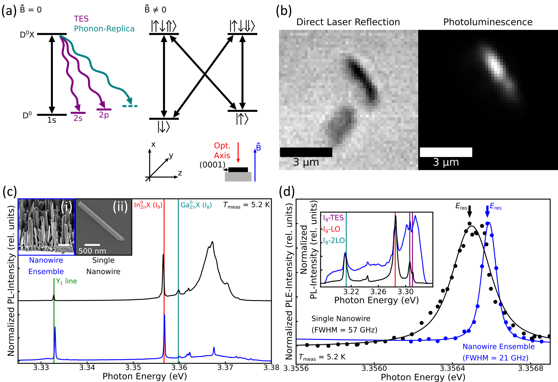
The energy level diagram of the In donor system is shown in Fig. 1a. The magnetic field lifts the spin degeneracy of the D0 and the D0X states due to the electron and hole Zeeman effects [22, 23, 21], respectively. This leads to four D0-D0X transitions with nominally two polarized in each and ; however, these polarization rules are relaxed when coupling into the end of a nanowire. Moreover, the system may relax via several lower energy transitions such as the longitudinal-optical (LO) phonon replicas and the two electron satellite (TES) transitions (corresponding to relaxation to an excited hydrogenic D0 orbital) [5].

Photoluminescence spectra of both the ensemble and single nanowire samples are shown in Fig. 1c. The In D0X transition is observed at 3.3567 eV. In addition to the In, Ga and Y-line donor-bound exciton features [5], the broad surface exciton is observed between 3.365-3.370 eV [24, 25, 26, 27]. The inset in Fig. 1d shows the In D0X TES and LO-phonon replicas under resonant In D0X excitation. A striking contrast can be observed between the two samples. In the ensemble sample, the TES and LO-phonon replicas are on a large background which is uncorrelated with the In D0X transition. This background may be related to the thin 2-dimensional layer of ZnO on the ensemble substrate as well as to the observed non-uniformity of individual nanowires. For single nanowire measurements, nanowires are screened for sharp In D0X transitions and low non-specific background in the TES/LO-phonon replica region [21].
The In D0X linewidth can be spectrometer-resolution limited. To obtain higher-resolution spectra, we perform photoluminescence excitation spectroscopy (PLE). In PLE measurements, D0X TES and LO-phonon replicas are monitored while tuning the excitation laser wavelength over the In D0X transitions. For the nanowire ensembles, the non-specific background is subtracted and only the LO-phonon replicas are monitored. The excitation power is 200 nW (7.2 µW) for the ensemble (single) nanowires. We are able to use a lower excitation power for the ensemble nanowires, because of the larger volume of material within our measurement spot and the increased collection efficiency from the top of the nanowires due to wave-guiding (see supplementary material [21]). As shown in Fig. 1d, in nanowire ensembles, PLE linewidths of 20 GHz are measured. These are comparable to the narrowest linewidths (15-25 GHz) measured in our lab on bulk single-crystalline ZnO for Ga D0X transitions at 5 K [21]. In single nanowires, linewidths as narrow as 57 GHz are observed. We attribute the increase in linewidth to additional strain caused by the dropcasting process as well as spectral diffusion and several homogeneous broadening mechanisms we will discuss further below. Due to the high non-specific background in the ensemble TES/LO-phonon replica region as well as the ability to isolate fewer donors in the isolated nanowires, we focus on single nanowire measurements for the remainder of this work.
In order to utilize the D0 system for quantum applications, the spin degeneracy of the D0 and D0X states must be lifted. A magnetic field may be used to split the ground state as determined by the electron -factor (). The splitting of the excited state is then solely determined by the hole -factor (), because the excited state electrons form a spin singlet. As shown in Fig. 2a, when a magnetic field is applied perpendicular to the crystal -axis, the sum of and is measured to be in a single nanowire. This is consistent with reported values for (1.9-2.0) and the lowest values reported for (0.1-0.3) [22, 23]. As described later in the text, we use high-resolution PLE to further confirm a of 1.90 and therefore a lower bound for of 0.07.
When a magnetic field is applied to the donor system, the spin degeneracy is lifted and donor spin initialization can be performed by resonant optical pumping [12, 13]. For example, to optically pump the system into the state, a resonant laser may be applied to the transition. Because the D0X state can relax into either D0 spin state [23], after several cycles, the spin is initialized to the state. Fig. 2b shows three PLE spectra which confirm that optical pumping can be achieved in a single nanowire. First, we perform a single-laser scan over the D0X transitions at 7 T (black data). Due to the small observed hole splitting, we expect the two transitions sharing the same electron spin ground-state level will not be resolved. For these single-laser, steady-state measurements, we also expect the PLE intensity to be significantly weaker at 7 T than it was at 0 T due to optical pumping. For the pair of transitions involving the state, the signal lies below the noise floor. To confirm that the overall low signal is due to optical pumping, we perform two-laser spectroscopy. A resonant pump laser is applied on the transition while a second probe laser is scanned over all the In D0X transitions (red data). In this two-laser PLE, the pump laser is able to re-pump population from to so that the transition signal is recovered. A similar phenomenon can be observed by placing the pump laser on the transition and recovering the transition signal (blue data). The 7 T two-laser linewidth of 55 GHz corresponds to the spectral diffusion and homogeneously broadened linewidth of the donor subpopulation that is optically pumped. This is within the uncertainty of the 57 GHz 0 T single nanowire PLE linewidth (Fig. 1d) which includes static inhomogeneous broadening from the entire donor ensemble. The similarity between the 0 T single-laser and the 7 T two-laser linewidths suggest broadening mechanisms, such as power broadening [28], laser-induced temperature broadening, and spectral diffusion that is fast compared to our measurement time (20 s) [29, 30, 31], are the dominant line broadening mechanisms in all of the single nanowire spectra. All of these mechanisms may be exacerbated by the higher powers used for single nanowire measurements relative to the ensemble nanowire measurements.
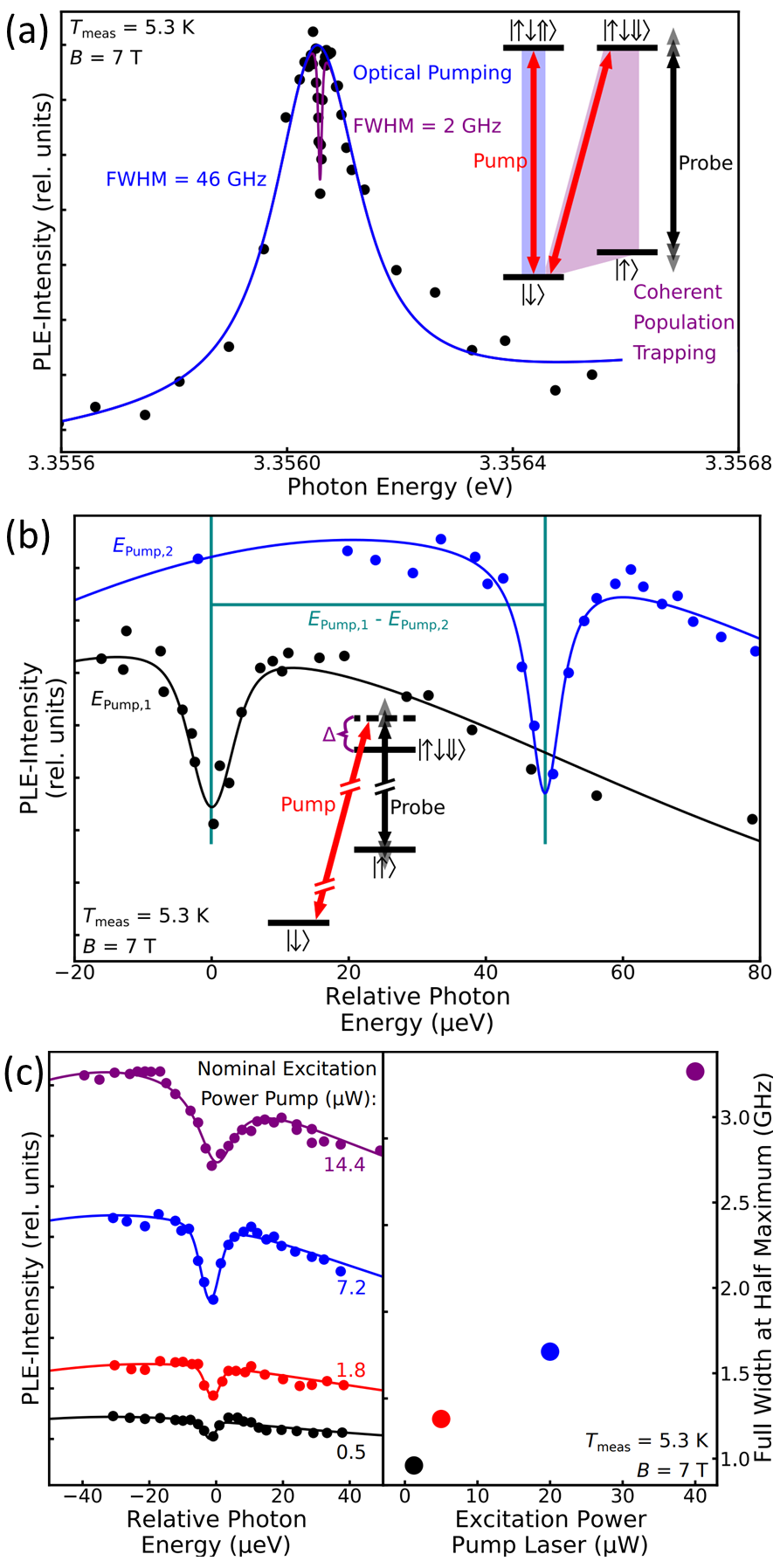
High-resolution two-laser scans, shown in Fig. 3a, reveal a sharp 2 GHz wide dip on the PLE peak that is the result of coherent population trapping (CPT). In CPT, the system enters a dark state when the two transitions of a system are simultaneously pumped [14, 15, 16, 17]. For example, the system can be formed between the two electron ground states and a single excited D0X state. In our experiments, because the Zeeman splitting between the D0X states is small relative to the two-laser linewidth (Fig. 2b), the pump laser is able to excite both and simultaneously; therefore, as shown in the inset to Fig. 3a, a system is formed by the pump laser driving and the probe laser on .
To confirm that the dip is related to CPT, we detune the pump laser energy by from and measure the shift of the dip (Fig. 3b). We observe a one-to-one correlation between and the spectral position of the dip [21]. As expected, the separation between the pump energies and the dip energies (0.76-0.77 meV) is consistent with a of 1.90 [23], confirming a lower bound for of 0.07. Moreover, Fig. 3c shows that reducing the pump laser power reduces the dip linewidth and contrast as expected in CPT [14, 32]. The smallest linewidth (1 GHz) approaches the linewidth expected due to the spin-9/2 In nuclear-electron hyperfine interaction, where the In line splits into 10 hyperfine lines separated by 100 MHz each [18, 19]. Moreover, considering spectral diffusion as a broadening mechanism for the two-laser peak (Fig. 2b), the narrowness of the CPT dip (1 GHz) compared to the two-laser peak (55 GHz) rules out ground-state spectral diffusion; therefore, excited-state spectral diffusion is the dominant spectral diffusion mechanism.
In summary, In donors in single ZnO nanowires preserve several important properties for utilizing donor spins in direct band gap materials as qubits. Photoluminescence excitation linewidths comparable to bulk show that even in the proximity of surfaces, high optical homogeneity is retained. Optical spin initialization and coherent population trapping are essential steps towards the spin control needed to prepare arbitrary qubit states. We expect higher collection efficiencies and cleaner selection rules can be achieved by moving towards single nanowires in a vertical geometry [21]. This would allow us to use lower excitation powers, minimizing the observed linewidth broadening and surface exciton. Additionally, there are several avenues to continue toward the single donor limit, including increasing the purity of the ZnO precursor materials or the study of two lattice-site donor defects, like the tin complex [33], that have lower probabilities of formation.
I Supporting Information
SEMs of ensemble nanowires, photoluminescence spectra of additional nanowires, description of background correction, 0 T photoluminescence spectra of the TES/LO-phonon replica region with resonant excitation, comparison of 0 T PLE on various samples, magnetic field dependent spectra to measure the g-factor in ensemble nanowires, photoluminescence spectra of the TES/LO-phonon replica region at 7 T with 2-laser resonant excitation, optical pumping demonstration of the nanowire ensemble and an additional nanowire, low-resolution 2-laser PLE measurements with varying pump wavelength, CPT measurements on an additional nanowire, CPT measurements on the main text nanowire with additional pump wavelengths, and simulation of light-guiding in a nanowire.
II Acknowledgements
We would like to thank Yusuke Kozuka for the bulk ZnO samples used for comparison, Ethan Hansen for assistance in performing PLE and PL measurements on ZnO nanowire ensembles, and Xiayu Linpeng for fruitful discussions. The support of the Natural Sciences and Engineering Research Council of Canada is gratefully acknowledged. This material is based upon work primarily supported by the Army Research Office MURI Grant on Ab Initio Solid-State Quantum Materials: Design, Production and Characterization at the Atomic Scale (18057522). Bulk measurements were supported by National Science Foundation under Grant No. 1150647.
References
- Tyryshkin et al. [2012] Alexei M. Tyryshkin, Shinichi Tojo, John J.L. Morton, Helge Riemann, Nikolai V. Abrosimov, Peter Becker, Hans Joachim Pohl, Thomas Schenkel, Michael L.W. Thewalt, Kohei M. Itoh, and S. A. Lyon, “Electron spin coherence exceeding seconds in high-purity silicon,” Nature Materials 11, 143–147 (2012).
- Saeedi et al. [2013] Kamyar Saeedi, Stephanie Simmons, Jeff Z Salvail, Phillip Dluhy, Helge Riemann, Nikolai V Abrosimov, Peter Becker, Hans-Joachim Pohl, John J L Morton, and Mike L W Thewalt, “Room-temperature quantum bit storage exceeding 39 minutes using ionized donors in silicon-28,” Science 342, 830–833 (2013).
- Wehner et al. [2018] Stephanie Wehner, David Elkouss, and Ronald Hanson, “Quantum internet: A vision for the road ahead,” Science 362 (2018), 10.1126/science.aam9288.
- Benjamin et al. [2009] Simon C. Benjamin, Brendon W. Lovett, and Jason M. Smith, “Prospects for measurement-based quantum computing with solid state spins,” Laser & Photonics Reviews 3, 556–574 (2009).
- Meyer et al. [2004] Bruno K. Meyer, H. Alves, D. M. Hofmann, W. Kriegseis, D. Forster, F. Bertram, J. Christen, A. Hoffmann, M. Straßburg, M. Dworzak, U. Haboeck, and A. V. Rodina, “Bound exciton and donor-acceptor pair recombinations in ZnO,” Physica Status Solidi (B) 241, 231–260 (2004).
- Khaetskii and Nazarov [2001] Alexander V. Khaetskii and Yuli V. Nazarov, “Spin-flip transitions between Zeeman sublevels in semiconductor quantum dots,” Phys. Rev. B 64, 125316 (2001).
- Ladd et al. [2010] T. D. Ladd, F. Jelezko, R. Laflamme, Y. Nakamura, C. Monroe, and J. L. O’Brien, “Quantum computers,” Nature 464, 45–53 (2010).
- Schmidgall et al. [2018] Emma R. Schmidgall, Srivatsa Chakravarthi, Michael Gould, Ian R. Christen, Karine Hestroffer, Fariba Hatami, and Kai Mei C. Fu, “Frequency control of single quantum emitters in integrated photonic circuits,” Nano Letters 18, 1175–1179 (2018).
- Schröder et al. [2016] Tim Schröder, Sara L. Mouradian, Jiabao Zheng, Matthew E. Trusheim, Michael Walsh, Edward H. Chen, Luozhou Li, Igal Bayn, and Dirk Englund, “Quantum nanophotonics in diamond [invited],” Journal of the Optical Society of America B 33, B65–B83 (2016).
- Kane [1998] B E Kane, “A silicon-based nuclear spin quantum computer,” Nature 393, 133–137 (1998).
- Ramdas and Rodriguez [1981] A K Ramdas and S Rodriguez, “Spectroscopy of the solid-state analogues of the hydrogen atom: donors and acceptors in semiconductors,” Reports on Progress in Physics 44, 1297–1387 (1981).
- Linpeng et al. [2016] Xiayu Linpeng, Todd Karin, M V Durnev, Russell Barbour, M M Glazov, E Ya Sherman, S P Watkins, Satoru Seto, and Kai-Mei C Fu, “Longitudinal spin relaxation of donor-bound electrons in direct band-gap semiconductors,” Physical Review B 94, 125401–125420 (2016).
- Sleiter et al. [2013] Darin J. Sleiter, Kaoru Sanaka, Y. M. Kim, Klaus Lischka, Alexander Pawlis, and Yoshihisa Yamamoto, “Optical pumping of a single electron spin bound to a fluorine donor in a ZnSe nanostructure,” Nano Letters 13, 116–120 (2013).
- Fu et al. [2005] Kai Mei C Fu, Charles Santori, Colin Stanley, M C Holland, and Yoshihisa Yamamoto, “Coherent population trapping of electron spins in a high-purity n-type GaAs semiconductor,” Physical Review Letters 95, 187405–187409 (2005).
- Santori et al. [2006] Charles Santori, Philippe Tamarat, Philipp Neumann, Jörg Wrachtrup, David Fattal, Raymond G. Beausoleil, James Rabeau, Paolo Olivero, Andrew D. Greentree, Steven Prawer, Fedor Jelezko, and Philip Hemmer, “Coherent population trapping of single spins in diamond under optical excitation,” Physical Review Letters 97, 247401–247405 (2006).
- Gray et al. [1978] H R Gray, R M Whitley, and C R Stroud, “Coherent trapping of atomic populations,” Optics Letters 3, 218–220 (1978).
- Xu et al. [2008] Xiaodong Xu, Bo Sun, Paul R. Berman, Duncan G. Steel, Allan S. Bracker, Dan Gammon, and L. J. Sham, “Coherent population trapping of an electron spin in a single negatively charged quantum dot,” Nature Physics 4, 692–695 (2008).
- Gonzalez et al. [1982] C. Gonzalez, D. Block, R. T. Cox, and A. Hervé, “Magnetic resonance studies of shallow donors in zinc oxide,” Journal of Crystal Growth 59, 357–362 (1982).
- Block et al. [1982] D Block, A Hervé, and R T Cox, “Optically detected magnetic resonance and optically detected endor of shallow indium donors in ZnO,” Physical Review B 25, 6049–6052 (1982).
- Kumar et al. [2013] E Senthil Kumar, F Mohammadbeigi, S Alagha, Z W Deng, I P Anderson, T Wintschel, and S P Watkins, “Optical evidence for donor behavior of Sb in ZnO nanowires,” Applied Physics Letters 102, 132105 (2013).
- [21] See Supplementary Material.
- Ding et al. [2009] L. Ding, B. K. Li, H. T. He, W. K. Ge, J. N. Wang, J. Q. Ning, X. M. Dai, C. C. Ling, and S. J. Xu, “Classification of bound exciton complexes in bulk ZnO by magnetophotoluminescence spectroscopy,” Journal of Applied Physics 105, 053511 (2009).
- Wagner et al. [2009] Markus R. Wagner, Jan Hindrik Schulze, Ronny Kirste, Munise Cobet, Axel Hoffmann, Christian Rauch, Anna V. Rodina, Bruno K. Meyer, Uwe Röder, and Klaus Thonke, “ valence band symmetry related hole fine splitting of bound excitons in ZnO observed in magneto-optical studies,” Physical Review B 80, 205203–205209 (2009).
- Wischmeier et al. [2006] L. Wischmeier, T. Voss, I. Rückmann, J. Gutowski, A. C. Mofor, A. Bakin, and A. Waag, “Dynamics of surface-excitonic emission in ZnO nanowires,” Physical Review B 74, 195333–195342 (2006).
- Biswas et al. [2011] Mahua Biswas, Yun Suk Jung, Hong Koo Kim, Kumarappan Kumar, Gregory J. Hughes, S. Newcomb, Martin O. Henry, and Enda McGlynn, “Microscopic origins of the surface exciton photoluminescence peak in ZnO nanostructures,” Physical Review B 83, 235320–235330 (2011).
- Grabowska et al. [2005] J. Grabowska, A. Meaney, K. K. Nanda, J. P. Mosnier, M. O. Henry, J. R. Duclère, and E. McGlynn, “Surface excitonic emission and quenching effects in ZnO nanowire/nanowall systems: Limiting effects on device potential,” Physical Review B 71, 115439–115446 (2005).
- Travnikov et al. [1989] V.V. Travnikov, A. Freiberg, and S.F. Savikhin, “Surface excitons in ZnO crystals,” Journal of Physics: Condensed Matter 1, 847–854 (1989).
- Reimer et al. [2016] M. E. Reimer, G. Bulgarini, A. Fognini, R. W. Heeres, B. J. Witek, M. A.M. Versteegh, A. Rubino, T. Braun, M. Kamp, S. Höfling, D. Dalacu, J. Lapointe, P. J. Poole, and V. Zwiller, “Overcoming power broadening of the quantum dot emission in a pure wurtzite nanowire,” Physical Review B 93, 195316 (2016).
- Holmes et al. [2015] M. Holmes, S. Kako, K. Choi, M. Arita, and Y. Arakawa, “Spectral diffusion and its influence on the emission linewidths of site-controlled GaN nanowire quantum dots,” Physical Review B 92, 115447–115454 (2015).
- Empedocles and Bawendi [1999] S. A. Empedocles and M. G. Bawendi, “Influence of spectral diffusion on the line shapes of single CdSe nanocrystallite quantum dots,” Journal of Physical Chemistry B 103, 1826–1830 (1999).
- MacQuarrie et al. [2021] Evan MacQuarrie, Camille Chartrand, Daniel Higginbottom, Kevin Morse, Valentin Karasyuk, Sjoerd Roorda, and Stephanie Simmons, “Generating T centres in photonic silicon-on-insulator material by ion implantation,” New Journal of Physics 23, 103008 (2021).
- Linpeng et al. [2021] Xiayu Linpeng, Todd Karin, Mikhail V. Durnev, Mikhail M. Glazov, Rüdiger Schott, Andreas D. Wieck, Arne Ludwig, and Kai Mei C. Fu, “Optical spin control and coherence properties of acceptor bound holes in strained GaAs,” Physical Review B 103, 115412–115422 (2021).
- Kumar et al. [2016] E. Senthil Kumar, F. Mohammadbeigi, L. A. Boatner, and S. P. Watkins, “High-resolution photoluminescence spectroscopy of Sn-doped ZnO single crystals,” Journal of Luminescence 176, 47–51 (2016).