Formation of graphene nanoribbons on the macrofacets of vicinal -SiC(0001) surfaces
Abstract
Thermal decomposition of vicinal -SiC(0001) surfaces with off-angles toward the direction results in the appearance of pairs of macroterraces and macrofacets covered with graphene, as follows. A carpet-like carbon layer grows on the surface, covering both the macroterraces and macrofacets; it forms buffer layer on the former ones, whereas its partial periodic bonding with the SiC steps on the latter ones generates a pseudo-graphene nanoribbon (pseudo-GNR) array. The nanoribbons have a width of 2 nm and are aligned in the direction with a spatial periodicity of 3.3 nm. Here, the Raman spectroscopy analysis of the pseudo-GNR array showed the absence of the 2D peak and the polarization dependence of the and peaks, which is typical of the armchair edge nanoribbon.
I Introduction
Graphene is a two-dimensional material with exotic electronic properties and very high carrier mobility, which makes it an interesting candidate for next-generation electronics a1 ; a2 . Application in traditional logic switching devices, however, requires the existence of a band gap that normal graphene lacks. Therefore, methods for opening a gap in the graphene band structure have been investigated. For example, cutting graphene into graphene nanoribbons (GNRs) with armchair edges can generate a substantial energy gap, but the ribbon width must be accurately controlled a3 ; a4 . Lithographyb1 and unzipping carbon nanotubesb2 are traditional top-down approaches to fabricate GNRs, while bottom-up approaches include GNR synthesis from molecular precursorsb3 ; b4 . Both strategies present some drawbacks, though; the top-down approaches struggle with accurate control of width and edge quality, while the bottom-up ones require specific metal substrates (i.e., the requirement of post-growth transfer procedure) and suffer in the ribbon alignment.
Today, GNR growth on semiconductor SiC substrates is attracting attention as a new bottom-up method. Through molecular beam epitaxy, an array of GNRs having nm width can be grown on the nanoperiodic structure c1 ; c2 formed on a vicinal SiC substrate c3 ; the resulting GNRs are periodic with nm spatial interval and exhibit a band gap of 0.14 eV, as observed via angle-resolved photoemission spectroscopy (ARPES). Graphene grown on a trench or mesa structures premade on SiC(0001) surfaces has also been studiedd1 ; d2 ; d3 ; d4 ; d6 ; d5 . The edge structure of GNRs grown on trench sidewall is controlled by trench orientation; specifically, the GNRs having zigzag edges grown on the sidewall along the direction of -SiC(0001) surfaces show the characteristics of ballistic conduction d1 ; d2 . Furthermore, both the zigzag-edge GNRs grown on the sidewall of -SiC(0001) surfacesd3 and the armchair-edge ones grown on -SiC(0001) surfacesd4 exhibit band gaps.
We previously have studied the formation and growth mechanism of graphene on terrace-facet periodic structures (reported as macrostep formation on vicinal SiC(0001) surfacese1 ; e2 ). Step bunching during thermal decomposition results in the formation of macroterraces and macrofacets with a period of several hundred nanomaters. Ienaga et al. f1 investigated bilayer graphene formed on macrofacets and observed the periodic modulation of electron-phonon coupling in the top graphene layer via scanning tunneling spectroscopy. This result suggests that the bottom carbon layer is not continuous graphene but an array of GNRs.
In the present work, we grew uniform single graphitic layer on macrofacets (hereafter defined as facet-graphene) and studied its structure and physical properties. This facet-graphene was attached periodically to the underlying substrate structures, and this repetition of freestanding portions of the carbon layer and those bonded to the substrate formed a pseudo-GNR array. Its Raman spectrum revealed features that are characteristic of armchair-edge GNRs and a width of several nanomaters.
II Experimental
A -SiC(0001) substrate with a miscut angle toward the direction was used to grow the GNR array. Such a large miscut angle was used to ensure a large facet/terrace area ratio, which is important for surace characterization via macroprobe methods such as low-energy electron diffraction (LEED) and ARPES; besides, the resulting low facet angle with respect to the surface is more accessible for scanning probe methods. First, the samples were cleaned and etched via high temperature annealing (C) in a hydrogen flow under atmospheric pressure. After confirming through atomic force microscopy (AFM) the surface morphology and the absence of polishing damage, we proceeded with surface thermal decomposition in an Ar atmosphere at ambient pressure and C; this treatment led to step bunching, resulting in a periodic surface morphology consisting of (0001) macroterraces and macrofacets (typically -inclined with respect to (0001)). The samples were then analyzed by AFM, LEED, scanning tunneling microscopy (STM), and microRaman spectroscopy.
III Results and Discussion
The AFM observation of the sample surace after thermal decomposition (Fig 1(a)) showed pairs of macroterraces and macrofacets, which had individual widths ranging from tens to nm, along the direction. The corresponding cross-sectional profile (Fig. 1(b)) revealed that the macrofacets formed an angle with respect to the (0001) macroterraces.
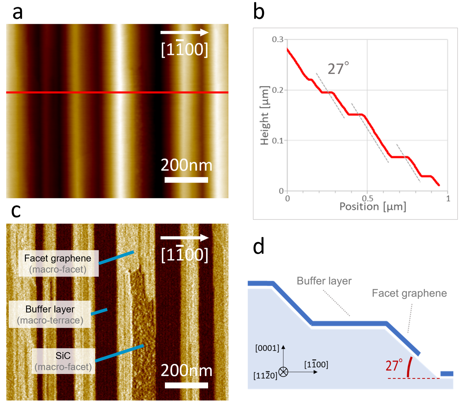
In the AFM phase image (Fig. 1(c)) of the same area, three types of regions of different contract could be clearly distinguished: dark areas on the macroterraces represent insulating buffer layer (hereafter denoted as 6R3)g1 ; g2 , and bright and grainy mid-tone areas, respectively paved and unpaved by graphene, on the macrofacets. The facet angle, as shown in cross-section (Fig. 1(d)) is related to the most energetically stable configuration, as reported in previous studiesd6 ; f1 . We will focus on the facet structures in the following paragraphs.
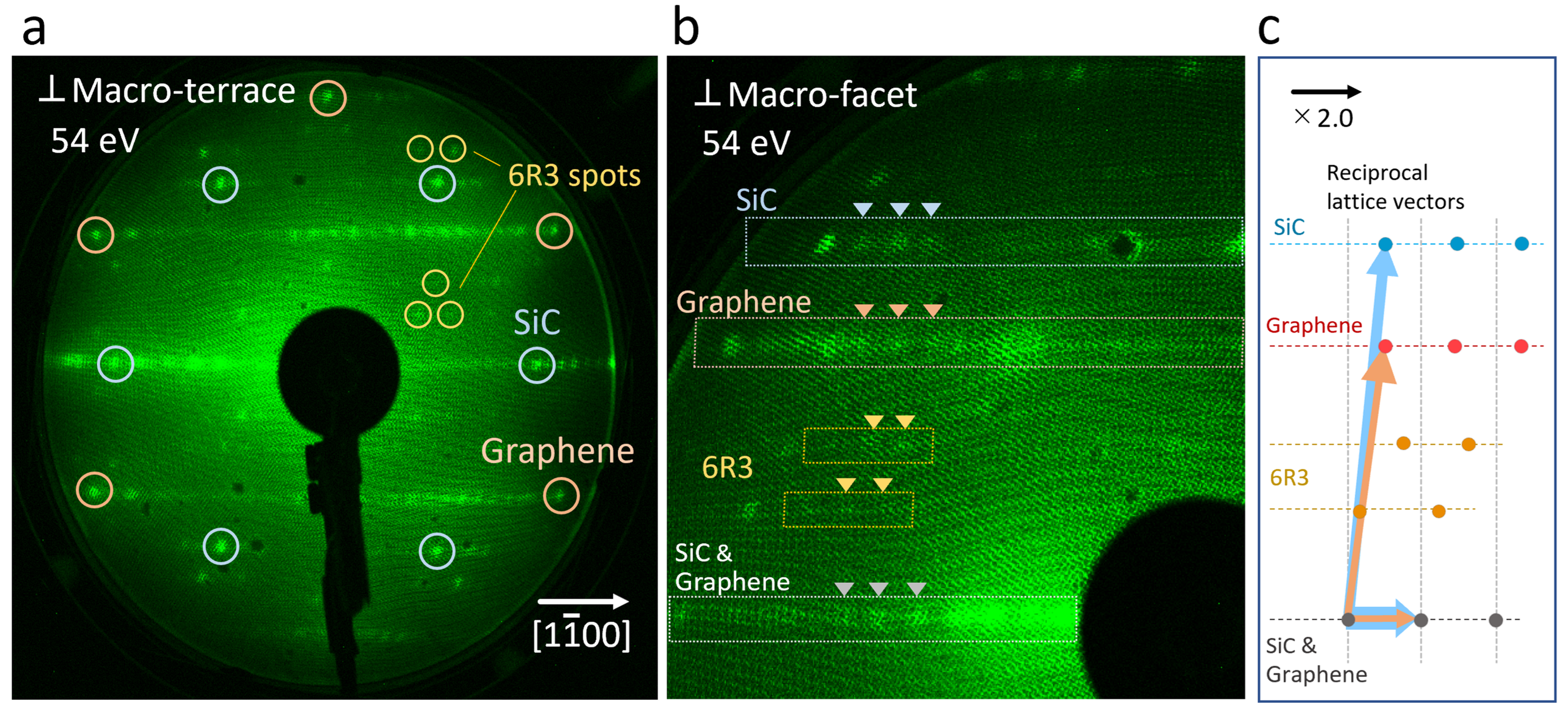
The LEED measurements were performed at two different incident beam directions, that is, normal to the macroterraces and macrofacets. In the first case (Fig. 2(a)), besides the typical spots of epitaxial graphene and SiC(0001) substrate and the satellite spots of the 6R3 buffer layer, chain like super-spots aligned along the direction were observed. When the electron energy was changed, these super-spots moved not only toward the center of the LEED pattern, as other major spots did, but also slid along the direction; this indicates that they came from the macrofacets and not from the macroterrace area. Indeed, when the sample was rotated , that is, when the beam was normal to the macrofacets, the movement of these super-spots with varying of the electron energy became focused toward the pattern center (Fig. 2(b)). In that case, the chain-like super-spots were observed around not only the main graphene spots but also the SiC and 6R3 reflexes. As will be discussed below, this was due to the moiré pattern between facet-graphene and SiC lattice along the direction. All the super-spots were equidistant and indicated a real-space periodicity of nm. Fig. 2(c) shows a diagram of the reciprocal cells corresponding to the observed periodic structures on the macrofacets.

Then, the macrofacets were studied by STM. An STM topographic image measured at a bias voltage of V (filled states) showed a bright and dark striped pattern along the direction (Fig. 3(a)). As shown by its cross-sectional height profile (Fig. 3(b)), the overall periodicity was nm, which coincides with the calculated spacing of the SiC LEED super-spots shown in (Fig. 2). The valley (darker) regions exhibited a fine structure with dot-like features lining up in the direction at an interval of nm, which is about six times the SiC lattice constant and coincides with the period of the 6R3 structure on SiC(0001) surfaces in the direction LEED-1 . Therefore, we assume that this is a one-dimensional moiré pattern between graphene and SiC lattice on macrofacets, similar to the 6R3 buffer layer. The LEED super-spots being lined up along the 6R3 spots in Fig. 2(b) also support this feature. Fig.3(c) shows the STM topographic image of the area outlined by the red frame in (a), taken at a lower bias voltage ( V), where the dot-like features in a valley can be observed more clearly; they formed a triple raw with a line spacing of nm, whose origin is discussed below.
Based on the AFM and STM results, we built a structure model of the macrofacet surface, having an angle of (Fig. 3(d)), which consists of miniterraces paired with and minifacets, corresponding to the ridges and valleys, respectively, in the STM image. The overall period is nm. These two characteristic minifacet angles arose because in -SiC(0001) a stacking sequence of Si-C bilayers is switched every three of them, resulting in locally different facet angles relative to (0001). In the minifacets, each row of carbon and silicon atoms is separated by 0.51-nm intervals, which is consistent with the dot-raw spacing observed in the STM image in Fig. 3(c).
We further investigated the stability of each minifacet under monolayer graphene. The and minifacets contain two and one dangling bonds per carbon atom, respectively, and thus are correspondingly more and less reactive to graphene. As a result, the graphene on each minifacet can exhibit different characteristics in both bonding configurations and electronic structure; these differences were indeed highlighted by the STM image shown in Fig. 3(c). A buffer-like graphitic layer was formed on the minifacets while quasi-freestanding graphene, in the form of nanoribbons, grew on the ones. In the following discussion, we define the bright and dark regions in Fig. 3(a) as pseudo-GNRs and buffer layer ribbons (BLRs), respectively; the term pseudo-GNRs (hereafter abbreviated just as GNRs), which continuously connect to BLRs, is used in contrast to isolated GNRs.
The samples were successively investigated via micro-Raman spectroscopy. Given the difficulty in extracting the Raman spectrum of the facet-graphene alone due to the limited spatial resolution ( m) of the equipment used, we prepared and analyzed two samples: one with a carbon layer covering the whole surface, i.e., both the macroterraces (in the form of the buffer layerRa-a1 ; Ra-a2 ) and macrofacets, and the other with a carbon layer only on the macroterraces (obtained at a reduced growth time) (Fig. 4(b)). Fig. 4(a) shows the measured spectra of both samples and the one of the facet-graphene alone, obtained by subtracting the blue spectrum from the red one. A Raman spectrum of graphene usually shows the , , and peaks. In this study, the peak, which is originated from the double resonance two-phonon inelastic scatteringRa-a5 , was absent. In the case of a narrow GNR, however, double inelastic scattering is much less probable than elastic scattering by the edges, rendering peak almost negligible and peak relatively high. This phenomenon has also been observed in other GNRs Ra-a3 ; Ra-a4 . Thus, the absence of the peak suggests the presence of narrow GNRs. In the and regions, three peaks components could be recognized (Fig. 4(a)).
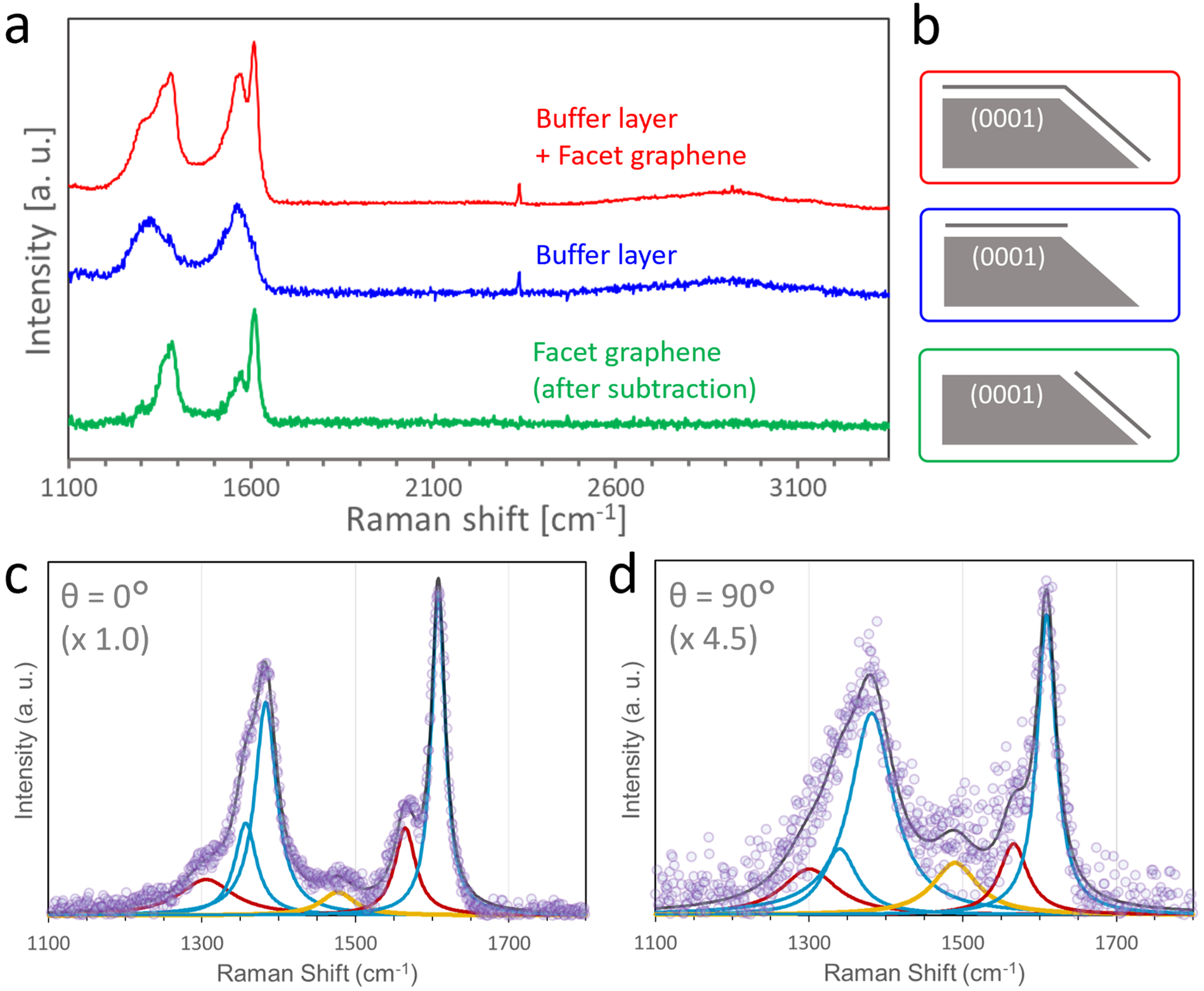
To better understand the spectral features, higher-resolution spectra were also measured at and , that is, with light polarization parallel and perpendicular to the GNR edges, respectively (Figs. 4(c,d)), revealing the light polarization dependence of the Raman spectra of the facet-graphene. The experimental spectra were fitted with six Lorentzian peaks, which were categorized into three origins: GNRs, BLRs, and an unknown component. The peaks having BLR origin were identified since their positions approximately matched the peaks in the 6R3 buffer layer on (0001) macroterraces observed in the blue spectrum in Fig. 4(a); they were attributed to a carbon sheet with bondings of BLRs (similarly to the 6R3 structure). The origin of the yellow peak at cm-1 was difficult to identify, but it may be associated with the edge-mode Ra-b3 . The curve with GNR origin consisted of three peaks: one peak at cm-1 and two peaks at cm-1. The latter ones were probably due to either the bulk- and edge-phonon contributions or the phonon energy difference depending on the scattering schemes for the -band transition. The peak was at a higher wavenumber compared with that for pristine graphene ( cm-1) reported by Lee et al.Ra-d1 We could not determine the cause of this blue shift, but it may be due to compressive strain, hole doping, or band gap openingRa-d1 ; Ra-d2 ; Ra-d3 . Band gap opening is the most plausible cause since our GNRs were nm wide and of the armchair-edge type, which results in a band gap larger than eV, based on the calculations Ra-d4 .
Finally, the polarization dependence shown in Fig. 4(c,d) indicates that the spectra at each angle were similar in shape but an intensity reduced by . This is a typical feature of armchair-edge grapheneRa-b1 ; Ra-b2 . All the Raman spectroscopy results described above confirm the formation of quasi GNR arrays on the macrofacets.
IV Conclusions
We studied graphitization phenomena on the macrofacets formed during thermal decomposition of vicinal -SiC(0001) surfaces with a relatively large miscut angle () toward the direction. The macrofacets were inclined by with respect to the (0001) macroterraces because of macrostep bunching and graphitization. Monolayer carbon was formed on the macrofacet surface and sectioned by GNR and BNR areas due to periodically striped surface structures. An array of aligned GNRs, each one having a width of nm and being lined up with a nm period, was identified.
The Raman spectrum of facet-graphene revealed the polarization dependence of the and peaks and the absence of the peak, confirming the existence of armchair-edge GNRs with narrow width. The GNRs were separated by BLRs, which implies that they were electronically isolated. The growth of a uniform pseudo GNR array on a semiconductor substrate via simple annealing is promising for applications in next-generation electronics.
References
- (1) A.K. Geim and K.S. Novoselov, The rise of graphene, Nature Mater. 6, 183 (2007).
- (2) K.S. Novoselov, Z. Jiang, Y. Zhang, S.V. Morozov, H.L. Stormer, U. Zeitler, J.C. Maan, G.S. Boebinger, P. Kim, and A.K. Geim, Room-temperature quantum hall effect in graphene, Science 315, 1379 (2007).
- (3) K. Nakada, M. Fujita, G. Dresselhaus, and M.S. Dresselhaus, Edge state in graphene ribbons: Nanometer size effect and edge shape dependence, Phys. Rev. B 54, 17954 (1996).
- (4) K. Wakabayashi, M. Fujita, H. Ajiki, and M. Sigrist, Electronic and magnetic properties of nanographite ribbons, Phys. Rev. B 59, 8271 (1999).
- (5) M.Y. Han, B. Özyilmaz, Y. Zhang, and P. Kim, Energy band-gap engineering of graphene nanoribbons, Phys. Rev. Lett. 98, 206805 (2007).
- (6) L. Jiao, L. Zhang, X. Wang, G. Diankov, and H. Dai, Narrow graphene nanoribbons from carbon nanotubes, Nature 458, 877 (2009).
- (7) L. Talirz et al., On-surface synthesis and characterization of 9-atom wide armchair graphene nanoribbons, ACS Nano 11, 1380 (2017).
- (8) J. Cai et al., Atomically precise bottom-up fabrication of graphene nanoribbons, Nature 466, 470 (2010).
- (9) H. Nakagawa, S. Tanaka, and I. Suemune, Self-ordering of nanofacets on vicinal SiC surfaces, Phys. Rev. Lett. 91, 226107 (2007).
- (10) M. Fujii and S. Tanaka, Ordering distance of surface nanofacets on vicinal 4H-SiC(0001), Phys. Rev. Lett. 99, 016102 (2007).
- (11) T. Kajiwara, Y. Nakamori, A. Visikovskiy, T. Iimori, F. Komori, K. Nakatsuji, K. Mase, and S. Tanaka, Graphene nanoribbons on vicinal SiC surfaces by molecular beam epitaxy, Phys. Rev. B 87, 121407(R) (2013).
- (12) J. Baringhaus, F. Edler and C. Tegenkamp, Edge-states in graphene nanoribbons: a combined spectroscopy and transport study, J. Phys.: Condens. Matter 25, 392001 (2013).
- (13) J. Baringhaus et al., Exceptional ballistic transport in epitaxial graphene nanoribbons, Nature 506, 349 (2014).
- (14) A.L. Miettinen, M.S. Nevius, W. Ko, M. Kolmer, A.-P. Li, M.N. Nair, B. Kierren, L. Moreau, E.H. Conrad, and A. Tejeda, Edge states and ballistic transport in zigzag graphene ribbons: The role of SiC polytypes, Phys. Rev. B 100, 045425 (2019).
- (15) A.A. Zakharov, N.A. Vinogradov, J. Aprojanz, T.T.N. Nguyen, C. Tegenkamp, C. Struzzi, T. Iakimov, R. Yakimova, and V. Jokubavicius, Wafer scale growth and characterization of edge specific graphene nanoribbons for nanoelectronics, ACS Appl. Nano Mater. 2, 156 (2019).
- (16) I. Palacio et al., Atomic structure of epitaxial graphene sidewall nanoribbons: Flat graphene, miniribbons, and the confinement gap, Nano Lett. 15, 182 (2015).
- (17) M.S. Nevius, F. Wang, C. Mathieu, N. Barrett, A. Sala, T.O. Mentes, A. Locatelli, and E.H. Conrad, The bottom-up growth of edge specific graphene nanoribbons, Nano Lett. 14, 6080 (2014).
- (18) T. Kimoto, A. Itoh, and H. Matsunami, Step bunching in chemical vapor deposition of 6H- and 4H-SiC on vicinal SiC(0001) faces, Appl. Phys. Lett. 66, 3645 (1995).
- (19) T. Kimoto, A. Itoh, and H. Matsunami, Step bunching mechanism in chemical vapor deposition of 6H- and 4H-SiC(0001), J. Appl. Phys. 81, 3494 (1997).
- (20) K. Ienaga et al., Modulation of electron-phonon coupling in one-dimensionally nanorippled graphene on a macrofacet of 6H-SiC, Nano Lett. 17, 3527 (2017).
- (21) K.V. Emtsev, F. Speck, T. Seyller, L. Ley, and J.D. Riley, Interaction, growth, and ordering of epitaxial graphene on SiC0001 surfaces: A comparative photoelectron spectroscopy study, Phys. Rev. B 77 (2008) 155303.
- (22) S. Kim, J. Ihm, H.J. Choi, and Y.-W. Son, Origin of anomalous electronic structures of epitaxial graphene on silicon carbide, Phys. Rev. Lett. 100 (2008) 176802.
- (23) F. Varchon, P. Mallet, J.-Y. Veuillen, and L. Magaud, Ripples in epitaxial graphene on the Si-terminated SiC(0001) surface, Phys. Rev. B 77 (2008) 235412.
- (24) F. Fromm, M.H. Oliveira Jr., A. Molina-Sànchez, M. Hundhausen, J.M.J. Lopes, H. Riechert, L. Wirtz, and T. Seyller, Contribution of the buffer layer to the Raman spectrum of epitaxial graphene on SiC(0001), New J. Phys. 15 (2013) 043031.
- (25) W. Strupinski, K. Grodecki, P. Caban, P. Ciepielewski, I. Jozwik-Biala, and J.M. Baranowski, Formation mechanism of graphene buffer layer on SiC(0001), Carbon 81 (2015) 63.
- (26) L.G. Cancado, M.A. Pimenta, R. Saito, A. Jorio, L.O. Ladeira, A. Grueneis, A.G. Souza-Filho, G. Dresselhaus, and M.S. Dresselhaus, Stokes and anti-Stokes double resonance Raman scattering in two-dimensional graphite, Phys. Rev. B 66 (2002) 035415.
- (27) R. Yang, Z. Shi, L. Zhang, D. Shi, and G. Zhang, Observation of Raman G-peak split for graphene nanoribbons with hydrogen-terminated zigzag edges, Nano Lett. 11 (2011) 4083.
- (28) A.N. Sokolov et al., Direct growth of aligned graphitic nanoribbons from a DNA template by chemical vapour deposition, Nat. Commun 4 (2013) 2402.
- (29) R. Saito, M. Furukawa, G. Dresselhaus, and M.S. Dresselhaus, Raman spectra of graphene ribbons, J. Phys.: Condens. Matter 22 (2010) 334203.
- (30) J.E. Lee, G. Ahn, J. Shim, Y.S. Lee, and S. Ryu, Optical separation of mechanical strain from charge doping in graphene, Nat. Commun. 3 (2012) 1024.
- (31) K. Sasaki, K. Kato, Y. Tokura, S. Suzuki, and T. Sogawa, Decay and frequency shift of both intervalley and intravalley phonons in graphene: Dirac-cone migration, Phys. Rev. B 86 (2012) 201403(R).
- (32) R. Gillen, M. Mohr, C. Thomsen, and J. Maultzsch, Vibrational properties of graphene nanoribbons by first-principles calculations, Phys. Rev. B 80 (2009) 155418
- (33) Y.-W. Son, M.L. Cohen, and S.G. Louie, Energy gaps in graphene nanoribbons, Phys. Rev. Lett. 97 (2006) 216803.
- (34) K. Sasaki, R. Saito, K. Wakabayashi, and T. Enoki, Identifying the orientation of edge of graphene using G band Raman spectra, J. Phys. Soc. Jpn. 79 (2010) 044603.
- (35) L.G. Cançado, M.A. Pimenta, B.R.A. Neves, M.S.S. Dantas, and A. Jorio, Influence of the atomic structure on the Raman spectra of graphite edges, Phys. Rev. Lett. 93 (2004) 247401.