Doping \ceMAPbBr3 hybrid perovskites with CdSe/CdZnS quantum dots: from emissive thin-films to hybrid single-photon sources
Abstract
We report the first doping of crystalline methylammonium lead bromide (\ceMAPbBr3) perovskite thin-films with CdSe/CdZnS core/shell quantum dots (QDs), using a soft-chemistry method that preserves their high quantum yield and other remarkable fluorescence properties. Our approach produces \ceMAPbBr3 films of 100 nm thickness doped at volume ratios between 0.025 and 5 % with colloidal CdSe/CdZnS QDs whose organic ligands are exchanged with halide ions to allow for close contact between the QDs and the perovskite matrix. Ensemble photoluminescence (PL) measurements demonstrate the retained emission of the QDs after incorporation into the \ceMAPbBr3 matrix. Ensemble photoluminescence excitation (PLE) spectra exhibit signatures of wavelength-dependent coupling between the CdSe/CdZnS QDs and the \ceMAPbBr3 matrix, i. e., a transfer of excitation energy from matrix to QD or from QD to matrix. Spatially-resolved PL experiments reveal a strong correlation between the positions of QDs and an enhancement of the PL signal of the matrix. Fluorescence lifetime imaging (FLIM) of the doped films furthermore show that the emission lifetime of \ceMAPbBr3 is slower in the vicinity of QDs, which, in combination with the increased PL signal of the matrix, suggests that QDs can act as local nucleation seeds that improve the crystallinity of \ceMAPbBr3, thus boosting its emission quantum yield. Confocal PL-antibunching measurements provide clear evidence of single-photon emission from individual QDs in perovskite. Finally, the analysis of blinking statistics indicates an improvement of the photostability of individual QDs in perovskite as compared to bare CdSe/CdZnS QDs. At high CdSe/CdZnS QD doping levels, this work opens thus the route to hybrid solar concentrators for visible-light harvesting and hybrid-based LEDs. Finally, low-doping content would lead to hybrid single-photon sources embedded in field-effect devices for single charge control to serve as an alternative to solid-state quantum dots and open the route to build nanophotonic devices with high-quantum-yield CdSe-based colloidal QDs.
keywords:
hybrid perovskites, colloidal quantum dots, single photon sources, nanocrystals, thin films1 INTRODUCTION
Research on hybrid perovskites for photovoltaics has been booming since 2009, evolving from the first reported efficiency of 3.8 % for a solar cell using perovskites as photo-active materials 1 to an efficiency of 28 in 20192. Since then, the literature and potential applications of hybrid perovskites have grown exponentially3, 4, 5, 6. In addition to their remarkable optical and transport properties, this success of hybrid halide perovskites is explained by them being easy to process and allowing to create multi-scale compounds (from bulk7 to thin-films8 and quantum dots (QDs) 9), as well as by their compatibility with industrially-scale soft-chemistry processes 5, 10. However, creating heterostructures with hybrid perovskites as active materials has so far remained an elusive goal. An important step to address this issue was recently taken with the use of hybrid perovskites (methylammonium lead iodide, MAPI) to create a host matrix for a different active material (PbS QDs) 11. However, this first QD-in-perovskite hybrid offers only limited perspectives for luminescence applications, on the one hand because PbS NCs emit in the infrared, which is not ideal for solar concentrators or LED applications and on the other hand because their low fluorescence quantum yield (QY) has so far not allowed the observation of single nano-objects, which would be essential for potential applications as single-photon sources (SPS). Following that first milestone, several promising ways to taking advantage of the properties of II-VI QDs and hybrid perovskites have been proposed: A thin film containing CdSe and \ceCsPbI3 QDs has been deposited on top of \ceMAPbI3 to study potential increases in conversion efficiency of perovskite-based solar cells 12. PbSe nanowires have been coated with \ceCsPbBr3 for applications as photodetectors 13. \ceCsPbBr3/CdS core/shell QDs with enhanced stability have been synthesized 14. Another recent example is the creation of \ceCsPbBr3/ZnS heterodimers and heterostructures to enhance stability 15. In spite of these important developments, no successful realization of CdSe-based QD-in-perovskite hybrid for luminescence applications has been reported so far to the best of our knowledge. CdSe colloidal quantum dots (QDs) are an economical, easy-to-tune, highly fluorescent active material 16, 17. The chemical synthesis of QDs is already established at the industrial scale and can be found in consumer products. Additional advantages of QDs are their tunable emission with nanosecond radiative recombination lifetimes and their tunable sheet density, which can be orders of magnitude higher than what is achievable by epitaxial growth. As a consequence, substantial research effort has been dedicated to CdSe QDs in LEDs18, solar cells19, 20, solar concentrators21 or as SPS and building blocks for quantum-information devices 22, 23, 24, 25. Unfortunately, the fragility of this class of emitters during encapsulation process 26, 27 and the lack of compatible semiconductor host matrices has rendered difficult their incorporation in crystalline, fast charge-transfer devices analog to what was achieved with state-of-the-art InGaAs diodes 28. The semiconductor nature of hybrid perovskites and the process compatibility between CdSe-QD synthesis and perovskite thin-film elaboration (soft chemistry) suggests that combining the remarkable properties of these two materials is an intrinsically interesting route for applications such as light converters (solar concentrator or LEDs at high doping level) and single photon sources (at low doping level). For the last two years, an intense effort has been put on coupling high quantum yield CdSe-based QDs with either organic or inorganic hybrid perovskite 3, 4, 5, 29, 30. So far, research has reported on either depositing CdSe QDs over a perovskite layer to enhance its light harvesting properties 30, or insertion of CdSe and \ceCsPbI3 in between a \ceMAPbI3 layer and a hole transport layer 29. However, to the best of our knowledge, none of the results reported so far was able to retain the fluorescence efficiency and single photon emission capability, which are actually the best assets of CdSe-based colloidal QDs.
In this article, we present the first emissive QD-in-perovskite hybrids in the visible range, based on thin \ceMAPbBr3 films doped with highly fluorescencent CdSe/CdZnS core/shell quantum dots. We present ensemble photoluminescence (PL) spectra demonstrating emission of these films at the CdSe/CdZnS wavelength. Photoluminescence excitation (PLE) experiments were performed, which demonstrate different types of response and coupling between the CdSe/CdZnS QDs and the \ceMAPbBr3 matrix. The combination of confocal PL microscopy and fluorescence lifetime imaging (FLIM) reveal sub-micron-scale correlations between the emission of the QDs and the \ceMAPbBr3 matrix. Finally, confocal PL microscopy demonstrates the first QD-in-perovskite hybrid single photon source emitting in the visible, with blinking properties enhanced compared to the non-encapsulated QDs.
2 METHODS
2.1 Quantum Dot Synthesis
CdSe/Zn1-xCdxS Colloidal quantum dots (CQDs) were synthesized following Refs. 31 and 32. To create the CdSe core, 15 mL of octadecene, 1 mmol of cadmium oxide and 3 mmol of myristic acid were introduced in a three-neck flask. The mixture was degassed at 60 ∘C under vacuum for ten minutes before being heated to 300 ∘C under argon. When the mixture became transparent, 0.25 mL of TOPSe at 2 M was introduced to react at 300 ∘C for three minutes. The ZnS shell was then created: 3 mL of zinc oleate (\ceZn(OA)2) at 0.5M and 1 mmol of dodecanthiol (DDT) were injected during one minute. The solution was then left to react 300∘C for 30 minutes. The shell created in this first growth step was composed theoretically of 60 % of Cadmium and 20 % of Zinc. Then, 2 mL of cadmium oleate (\ceCd(OA)2) at 0.5 M, 4 mL of \ceZn(OA)2 at 0.5 M and 1.5 mL of TOPS at 2 M were injected in one minute, resulting in a final shell that was equal parts cadmium and zinc. This mixture was heated during 10 minutes to 300 ∘C. This step was repeated 4 times and for each injection, a few nanometers of shell were created. The synthesized QDs were eventually dispersed in hexane.
2.2 Ligand Exchange
To transfer the CQDs in the perovskite precursor solvent, which is N,N-Dimethylformamide (DMF), an OA-to-halide ligand exchange was necessary. To this end, 60 µL of CQDs were injected into 2 mL of hexane containing 1 mL of methylammonium bromide (0.2 M) and cadmium bromide (0.3 mmol). This solution was stirred until the QDs were transferred from hexane to DMF, at which point they were precipitated with isopropanol and redispersed in DMF two times. In the end, CQDs with bromide ligands were dispersed in DMF (2 mL) and 1 mL of methyammonium chloride (0.1 M) then the solution was sonicated for 25 minutes at 50 ∘C. An extensive optical characterization of the obtained halide-covered CdSe/CdZnS QDs can be found in Ref. 32.
2.3 QD-in-Perovskite Heterostructures
Thin-film QD-in-perovskite heterostructures were created by spin-coating a solution of perovskite precursor and halide-ligand QDs onto a glass (BK7) slide: 100 µL of perovskite precursor solution at 1 M and 100 µL of QDs with the appropriate concentration were spin-coated at 5000 rpm during 60 seconds; 5 seconds after the start, 1 mL of chlorobenzene was injected.
2.4 Ensemble spectroscopy
PL and PLE experiments were performed with an FS5 spectrofluorometer (Edinburgh Instr.) at 405 nm excitation wavelength for the PL spectra, and 645 nm detection for PLE measruements. Resolution for both experiments was set at 1 nm, and integration time per point at 300 ms and 1 s for PL and PLE respectively.
2.5 Spatially Resolved PL/FLIM Measurements
Spatially resolved measurements were performed with the home-built confocal microscope described in Ref. 33. Images were recorded with an oil-immersion objective (Olympus NA=1.35, x60) which focused a pulsed laser-light (Edinburgh Instr. EPL0450) at 445 nm and 2 MHz repetition rate, and collected the emitted signal. The intensity used was 50 W/cm2 for sample A, and 150 W/cm2 for sample B. The images are presented as the sum of 10 consecutive scans with 100 ms integration time per pixel per scan. The images were corrected for the small in-plane drift of less than 2 pixels that occurred during the measurements. Detection was assured by two single-photon avalanche photodiodes (SPADs), an ARQH-050 (Perkin Elmer) for QD luminescence and a Count-20 C (Laser Components) for the \ceMAPbBr3 signal; these detectors were connected to a time-correlated single-photon counting card (TimeHarp 200 with router, PicoQuant). The Bandpass filters used for selective detection were a combination of an FBH0650 (Thorlabs) with a BrightLine 655 (Semrock) for QD emission and a 65-700 (Edmund Optics) with an OD=1 neutral density filter for the \ceMAPbBr3 signal.
2.6 Individual QDs in Perovskite
Measurements were performed using the same home-built set-up,. Antibunching and blinking measurements were performed with a cw laser excitation at 561 nm (Exelitas). A bandpass filter (Thorlabs FBH0650 and Semrock BrightLine 655) was placed in front of both SPADs to select the emission of individual QDs in the QD-in-perovskite hybrid for the antibunching measurements.
3 RESULTS AND DISCUSSION
3.1 Undoped Perovskite Thin Films
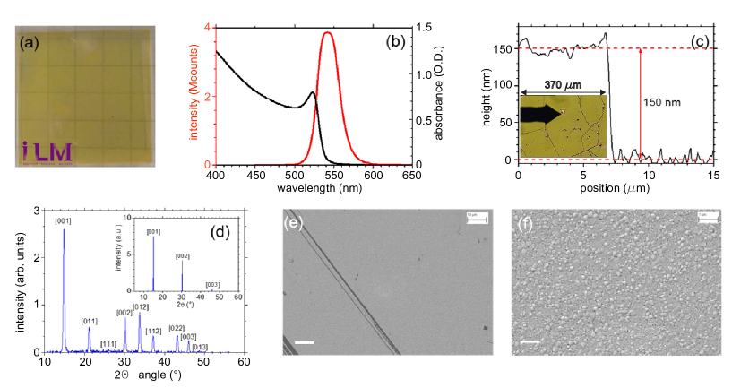
We present in Fig. 1 optical and structural characterizations of undoped \ceMAPbBr3 films. Figure 1 (a) shows a photograph of a typical film obtained with the protocol detailed in Methods: transparent-orange, indicating absorption in the visible and low-diffusing behavior as a hint to a good crystallinity. The absorption spectrum of the same sample, Fig. 1 (b), exhibits a strong and narrow absorption peak at 520 nm typical of an \ceMAPbBr3 exciton 34. The corresponding photoluminescence (PL) spectrum shows a narrow emission peak centered at 540 nm, with a full width at half-maximum (FWHM) of 35 nm. We note that the emission is actually structured by two peaks at = 533 and 544 nm, with intensity ratio varying over different region of the sample. The emission at 533 nm is attributed to the band-edge free exciton 35, 36, 37, and the emission at 544 nm to shallow defects near the \ceMAPbBr3 band-edge 36, 38. Surprisingly, the shallow defects do not have a signature in the \ceMAPbBr3 absorption spectrum, but the unambiguous detection of their emission points to a vanishing absorption coefficient and their emission being activated via charge relaxation from the \ceMAPbBr3 band-edge exciton 36, 37. Atomic force microscopy (AFM) of the film reveals a thin-film thickness of 150 nm, Fig. 1 (c). Fig. 1 (c) is an AFM profile taken from a crack on the sample surface presented in the optical microscope picture in the inset of Fig. 1 (c) (the dark region is the shadow of the AFM cantilever). Thickness measurement were performed on 8 samples and returned an average thickness of 152 nm. This is the average thickness measured on undoped \ceMAPbBr3 thin-films, created with 1 M concentration of the precursor. The protocol to insert the QDs leads to a 0.5 M concentration of the perovskite precursor and average doped film thickness of 100 nm. Figure 1 (d) presents an X-ray diffraction diagram of the sample in Fig. 1 (a, b) realized under grazing incidence; peaks are labelled according to the crystallographic planes of \ceMAPbBr3. The inset in Fig. 1 (d) presents the diffraction diagram in standard geometry, in which only directions with , 2 and 3 contribute, indicating a strong orientation of the thin film along those axes. The crystallization of the film thus occurs without any annealing step, but is induced by the injection of the chlorobenzene counter-solvent at 4 s after the spin-coating started 39, 40. We present in Fig. 1 (e) a scanning electron microscopy (SEM) image of the sample over a 110x76 µm2 region, showing an homogeneous surface with occasional straight-line cracks, with an AFM-measured depth of 150 nm (Fig. 1 (c)). A more resolved SEM picture over a region of 11x7.5 µm2, Fig. 1 (f), shows the crystallite fine structure, with sub-micron size. The arrangement suggests for a compact thin film of \ceMAPbBr3.
3.2 QD-in-perovskite hybrid: ensemble measurements
Figure 2 (a) shows the photoluminescence (PL) spectra of three different \ceMAPbBr3 thin films doped at 0.1, 0.5, and 5 % with CdSe QDs. The spectra are normalized to their respective perovskite maximum emission. The luminescence of the QDs can be observed even at a doping level of 0.1 %, centered at 638 nm, with an emission linewidth of 43 nm. Increasing the doping level to 0.5 and 5 % increases the QD luminescence with respect to the perovskite matrix emission, confirming that emission survives from low to high doping levels. The emission wavelength and the full width at half maximum (FWHM) remain unchanged at 638 nm and 43 nm respectively for all doping levels. On the other hand, the center emission wavelength of the QD-in-perovskites hybrid is red-shifted to the red by 4 nm compared to QDs in air, Fig.2 (b). We attribute the shift to the heteroepitaxial relationship between the perovskite and the QDs created at the hybrid interface, in which the surrounding perovskite acts a shell to modify the potential barrier seen by the exciton.
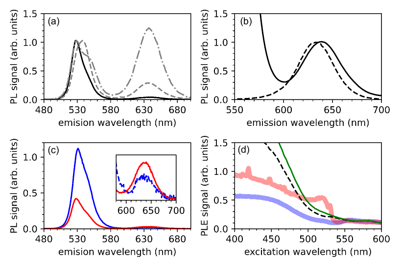
We present in Fig.2 (c) the PL spectra of two CdSe/CdZnS-doped thin films: Sample A (blue) and sample B (red), prepared under conditions corresponding to a nominal doping of 0.025 and 0.1 %, respectively. The two spectra are comparable, with strong \ceMAPbBr3 emission around 530 nm and a weaker QD contribution centered at = 638 nm (see inset in Fig.2 (c)). Photoluminescence excitation (PLE) spectra on sample A and B, detected at the QDs emission wavelength ( nm) are shown in Fig. 2 (d), with two reference spectra, QD on glass on the one hand and, on the other hand, the expected PLE of a hypothetical interaction-free \ceMAPbBr3 film doped homogeneously with QDs. The first noticeable feature of these results is the difference between the PLE obtained from sample A and sample B. The second highlight is the strong deviation of these two PLE spectra from what is expected from QDs in a \ceMAPbBr3 matrix in the absence of coupling. To help quantify and explain these differences, we introduce the quantity :
| (1) |
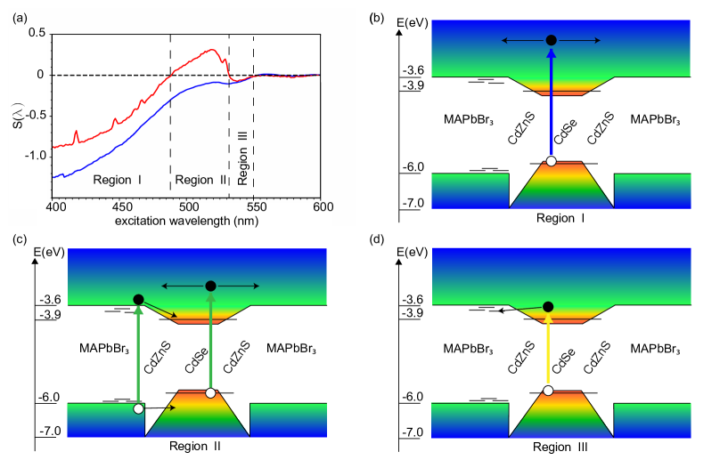
where is the experimental PLE spectrum of sample A and B, respectively. The expected PLE spectrum for QDs in \ceMAPbBr3 without any interaction between them and the host matrix is , where represents the measured PLE spectrum of bare QDs on glass, while and stand for the absorption coefficient and the thickness of the \ceMAPbBr3 host matrix respectively. Given this definition of , we expect for samples in which the QDs do not interact with the host matrix, while indicates an exchange of energy between the matrix and the QDs. As can be seen in Fig. 3 (a), there are indeed two main wavelength zones: one in which for nm, which corresponds to the transparency region of the perovskite where we do not expect coupling between the QD and the \ceMAPbBr3 matrix, and another one with for nm, which is the absorbing region of the \ceMAPbBr3 matrix. We can furthermore distinguish three regions in that latter zone, Region I ( nm), II ( nm) and III ( nm). In Region I, we find for both sample A and B, meaning that coupling between the QD and the perovskite occurs such that it leads to a less efficient QD emission. We explain this signal-decrease in Fig. 3 (b), where we indicate the ancillary relaxation paths of an electron promoted to the conduction band of QDs in perovskite that are not available in the absence of the matrix. While the main relaxation path of the electron for the bare QDs leads to the QD conduction band edge, the hybrid sample makes it becomes possible for the electron to be delocalized in the perovskite matrix. This effect gets stronger as the excitation energy is increased, since the probability to fall- back in the QD decreases. In Region II, the optical response of sample A and B are different: while . QDs in sample A lose signal to the perovskite, by the same mechanism as in region I, while QDs in sample B gain signal from the perovskite. Figure 3 (c) proposes a scenario in which coupling between the QDs and the perovskite matrix can lead to an increase of the QD signal: The putative band alignment of our QD-in-perovskite system suggests that Region II could correspond to the creation of excitons at the \ceMAPbBr3 band edge ( nm), and that these excitons can actually be transferred to a nearby QD by electron relaxation and hole tunneling. This process could be conceptualized as the surrounding perovskite acting as a shell for the QD, increasing its effective absorption cross-section for wavelengths in Region II, leading to a competition between the effects described for Region I (Fig. 3 (b)) and Region II (Fig. 3 (c)), which is sample-dependent. We speculate that the local hetero-epitaxial arrangement between the QDs and the perovskite matrix might be different for sample A and B, leading to different contributions of the two coupling phenomena (from QD to matrix vs. from matrix to QD). Since the crystallization of the compound highly depends on the timing of the chlorobenzene injection, which is carried out manually, it is not surprising that small discrepancies from sample to sample can lead to differences in the QD-perovskite interface; further investigation will be necessary to achieve a deeper understanding of this phenomenon. In Region III, both sample A and B exhibit comparable behavior with . This is surprising at first since Region III is mostly transparent if one looks at the \ceMAPbBr3 absorption spectrum (Fig. 1 (b)). However, the \ceMAPbBr3 and sample A and B emission spectra, clearly exhibit a sub-band-edge contribution that we attribute to the emission of shallow defects 37, 41. These defects do not show a clear signature on the absorption spectra, implying a small absorption cross-section. However, their presence close to the \ceMAPbBr3 band-edge could allow tunneling of an electron out of the QD to these defects states, lowering the QD emission signal when excited in Region III of the spectrum, as depicted in Fig. 3 (d). Confirming these explanations would require further studies, which should include variation of the \ceMAPbBr3 matrix composition with \ceCl and \ceI halides to vary the band structure.
3.3 QD-in-Perovskite Hybrid: Spatially Resolved Measurements
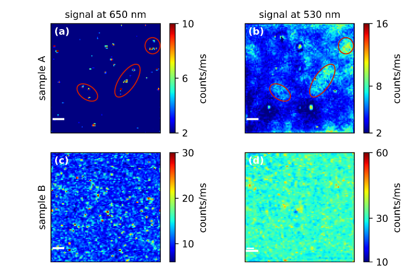
Figure 4 shows confocal photoluminescence images of a 5050 µm2 region of sample A (Figs. 4 (a) and (b)) and sample B (Figs. 4 (c) and (d)); these images were recorded simultaneously at the \ceMAPbBr3 and the QD emission wavelengths for both samples with pulsed-laser excitation (445 nm, 2 MHz repetition rate). Comparing the images obtained at the QD emission wavelength ( nm, Figs. 4 (a) and (c), we find that sample A features small QD clusters (sub-micron size) with a rather low density, while sample B shows a more homogeneous distribution of the QDs with a larger signal. That latter property is coherent with the PLE signal of sample A and B presented in Fig. 2 (d) where the relative signal of the QDs excited at nm is only about half for sample A as compared to sample B. We expect, however, from the nominal doping of the sample A (0.025 %) and sample B (0.1 %) a smaller QD density in sample A. Focusing now on the signals recorded at the \ceMAPbBr3 emission wavelength of () nm, Fig. 4 (b) and (d), we find a surprisingly correlated behavior between the perovskite and the QD emission: an homogeneous spatial distribution of the PL signal for sample B (Fig. 4 (d)), while the perovskite emission is structured for sample A (Fig. 4 (b)). It is rather straightforward to recognize that the \ceMAPbBr3 emission signal in sample A increases at the locations of QD clusters with an almost one-to-one correlation with the QDs positions. Red ellipses in Fig. 4 (a) and (b) indicate a few examples of such correlations. The influence of the QDs on the emission of the \ceMAPbBr3 matrix extends over a length scale of approximately 2 µm, while the size of the QD clusters lies in the sub-micron range. At the higher QD density of sample B, an interaction that extends over around 2 µm produces a homogeneous image at the \ceMAPbBr3 emission wavelength. Our tentative interpretation of this behavior is that the QDs act as crystallization seeds for the \ceMAPbBr3 matrix. Regions of better crystallinity exhibit higher emission QY and thus lead to a higher PL signal. If this hypothesis is correct, one would also expect an increase of the \ceMAPbBr3 emission lifetime at the location where the crystallinity of the matrix is increased (leading a smaller amount of defects).
3.4 QD-in-Perovskite Hybrid: Fluorescence-Lifetime Imaging Microscopy
We present in Fig. 5 fluorescence-lifetime imaging measurements (FLIM) of samples A (Fig. 5 (a)) and B (Fig. 5 (b)) obtained at the \ceMAPbBr3 emission wavelength, covering the same regions as shown as in Fig. 4. Every pixel contains a lifetime curve which is fitted by a bi-exponential function with background, including convolution with the instrument response function (IRF):
| (2) |
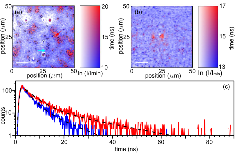
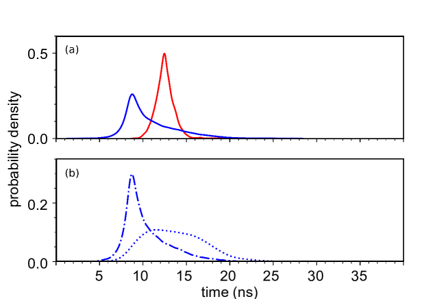
where is the background, and the short and long lifetimes, respectively, and and the associated amplitudes; the values of the slow component are represented in the FLIM images. The scale of these images enables an original presentation of the data with double color scaling: the saturation of the colors indicate the intensity level (white colors indicate minimum photon counts, while a saturated blue or red corresponds maximum of signal), while the colors themselves represent lifetime (blue is faster, red is slower). Fig. 5 (a) shows that the regions where the QDs are located (indicated by dashed circles) exhibit a longer lifetime (red pixels) of the \ceMAPbBr3 emission as compared to QD-free zones (dominated by a blue color). Fig. 5 (c) presents two decay curves, one taken from the red pixel at the location indicated by the red arrow in Fig. 5 (a), the other from the blue pixel indicated by the light-blue arrow in Fig. 5 (a). The bi-exponential fits, taking into account the instrument response function, are shown as black dashed-lines in Fig. 5 (c) and yield a long component at = 15 ns for the red pixel (close to a QD), and = 9 ns for the blue pixel (QD-free region). Fig. 5 (b) (sample B) shows a more homogeneous lifetime distribution than Fig. 5 (a), covering a smaller dynamical range and dominated by blue pixels. These results are compatible with our hypothesis that QDs locally modify the crystallinity of the \ceMAPbBr3 matrix, provoking a local change in the emission lifetime. We present in Fig. 6 (a) the distribution of the lifetimes obtained from the pixels of Fig. 5 (a) (sample A, blue line) and (b) (sample B, red line). The lifetime distribution in sample A is highly skewed toward the long-lifetime tail, peaking at 8.5 ns and extending to more than 20 ns. On the contrary, the lifetime distribution in sample B is an almost symmetric super-Gaussian (leptokurtic) curve centered at 13 ns with a FWHM of ns. In order to unravel the lifetime distribution of sample A as a function of QD presence, we have separated the pixels of the lifetime image, Fig. 5 (a), based on an intensity-threshold criterion for the image of the QD luminescence of the same sample, see Fig. 4 (a). As can be seen in Fig. 6 (b), the distribution of lifetimes found for pixels exhibiting strong QD luminescence (dotted blue line) differs significantly from the one in regions of low QD signal (dash-dotted blue line): The short lifetimes making up the peak at 8.5 ns are associated with the areas of the \ceMAPbBr3 matrix that do not contain many QDs, while a broader distribution with a median value of 14 ns corresponds to the QD-rich regions. We furthermore note that the median value of the lifetime distribution from QD-rich pixels in sample A corresponds to the maximum of the lifetime distribution found in sample B, which shows a stronger and spatially homogeneous QD signal. These results, showing an increased emission lifetime of the \ceMAPbBr3 matrix at the QD locations, corroborate our speculative interpretation that the QDs act as local seeds of the \ceMAPbBr3 host and help to locally improve crystallinity.
3.5 Single QDs in Perovskite
Having in sight single photon sources applications22, we present in Fig. 7 (a) and (b) confocal images of another region of sample A obtained at an excitation wavelength of 561 nm and recorded simultaneously at the \ceMAPbBr3 (a) and QD (b) emission wavelengths. The perovskite image shows a noisy unstructured signal over the 1010 µm2 area (as expected when for excitation in its transparency region), while the QD image is structured with resolution-limited (200 nm) high-emission spots. We performed photon-coincidence measurements at short times of the signal originating from these spots using a Hanbury Brown and Twiss (HBT) interferometer; a typical result can be seen in Fig. 7 (c). The curve shows clear antibunching behavior, characteristic for the emission of an individual quantum system acting as a single-photon source. Measuring the signal of a single QD without difficulties (integration time in Fig. 7 (b) is 1 ms/pixel) is further testament to the conservation of the fluorescence quantum yield during the doping process: At high excitation intensity, we registered up to 800 000 counts/s from a single emitter in the QD-in-perovskite hybrid, Fig. 7 (d). We performed a statistical analysis of 47 single QDs and fitted the obtained functions with a single exponential rise functions22 :
| (3) |
We extract an average rise time of the QD-in-perovskite hybrid of ns. Details of the fitting procedure can be found in Ref. 32. We compare this average rise time to the antibunching obtained from 14 single CdSe/CdZnS QDs deposited on glass, for which the same analysis yields an average time of ns. Since we detect up to 800 000 photons/s from a single QD in perovskite, we do not consider this reduced rise time as the consequence of the opening of new non-radiative recombination channels, i.e., a decrease of the emission quantum yield. Rather, we attribute it to the increase of the refractive index surrounding the QDs, from QDs in air deposited on a glass slide, to QDs embedded in a \ceMAPbBr3 matrix. It has been demonstrated that CdSe/ZnS QDs can be used as probe of the local refractive index of their environment, with a sphere of sensitivity of radius nm49, 50, and that their decay time in a \ceSiO2 matrix follow those predicted by an effective medium model33. We use the virtual cavity (VC) model which can be written as:
| (4) |
| (5) |
where , and are the exciton recombination rates of CdSe/CdZnS QDs spincast on a glass coverslip, in the \ceMAPbBr3 matrix and in vacuum, respectively, while and are the effective refractive indices experienced by QDs on glass and in the \ceMAPbBr3 matrix. For the reference sample () we find , while the effective refractive index for the QD-in-perovskite heterostructure (, = 2.10, determined by ellipsometry at 650 nm) is , considering an homogeneous distribution of the QDs in the thin-film. Inserting and ns-1 (from the measured ns) into the VC model of Eq. (4), we obtain ns-1, which corresponds to an exciton recombination lifetime in vacuum of ns. The value of thus identified leads to an expected radiative lifetime for the QD-in-perovskite hybrid of ns when used in Eq. (5), which corresponds to our experimental value. This estimate was obtained with a assumed radius of influence of nm, in accordance with our previous results on CdSe-based QDs51, 50, 33 ranging between 50 and 100 nm. We therefore consider this feature as another proof that the QDs have been integrated to the perovskite matrix and that we are able to observe single QDs in perovskites as efficient single photons sources in the visible range.
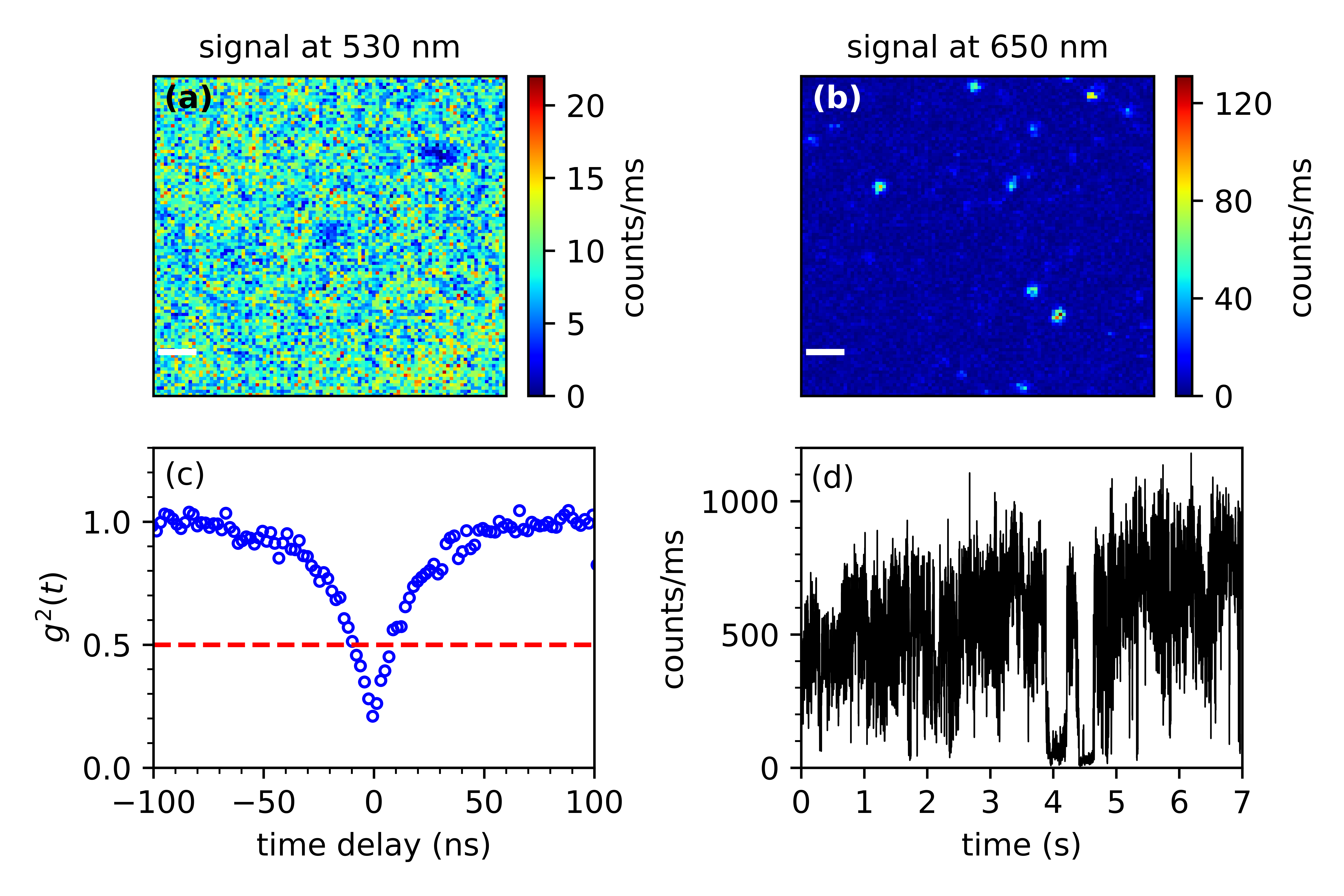
Having identified single QD-in-perovskite hybrids, we studied their blinking properties, as compared to CdSe/CdZnS QDs on glass. The details of the blinking analysis technique, presented on the QDs with OA ligands, have been published elsewhere32. Blinking statistics were recorded under the same excitation conditions for both the single QD-in-perovskite hybrids and the OA-capped QDs: and . We compare the results obtained on 11 single QD blinking from sample A and 24 single QDs with OA ligands deposited on glass. We find that the median proportion of ON times for QD-in-perovskite is as large as 99 %, and stands at 81 % for OA-capped reference QDs. This particularly large number for single QDs in perovskite is sample dependent, and we found it to be 94 and 96 %, respectively, on two other samples of QD-in-perovskites. This small variability of the results surely depends on a lot of factors, crystallisation being probably an important one; nevertheless, we found that encapsulated single QDs in hybrid perovskite show a consistent improvement of their blinking statistics with the median time spent in the ON state increasing in all three samples compared with the reference OA-capped QDs. Optimization of the blinking statistics by tuning deposition conditions will require further studies, but we identify the present results encouraging as a first step toward the control of blinking.
4 CONCLUSION
In conclusion, we have detailed a soft-chemistry method to realize the first doping of \ceMAPbBr3 thin films with halide-capped (\ceCl and \ceBr) CdSe/CdZnS QDs emitting in the visible. The QD shell needed a high ratio of Zn to avoid potential cation exchange between Cd and Pb ions of the matrix. A ligand-exchange procedure was developed, which removed the initial organic ligands (OA) and replaced them with halide ions, thus ensuring a direct and stable mixing of the QDs in DMF with the \ceMAPbBr3 precursors. The obtained QD-in-perovskite films were 100 nm thick on average, with cubic crystalline structure. Different CdSe/CdZnS doping levels were explored down to 0.025 % doping, ensemble PL spectra revealed the presence of emitting QDs at 638 nm in the doped films. We focused our study on two samples (0.1 and 0.025 % doping level) processed under the same nominal conditions which produce comparable PL spectra, while their PLE was found to be substantially different. Their PLE spectra were explained with three additional relaxation processes, occurring in three wavelength regions. First, at high excitation energy, relaxation channels of the electrons from the QDs are open in the \ceMAPbBr3 matrix; second, at an excitation energy around that of the \ceMAPbBr3 exciton, this energy can be transferred to the QDs to increase their emission signal; and finally, in a narrow energy region where shallow defects of the \ceMAPbBr3 matrix exist, electrons can be transferred from the QDs to those defects. Local PL measurements in confocal geometry show that the \ceMAPbBr3 matrix emission signal increases at the QD locations in our doped thin-films, pointing toward a better crystallinity triggered the inclusion of the QDs, which could act as seeds in the \ceMAPbBr3 crystallization process. The influence radius of the QD seeds on the \ceMAPbBr3 is estimated to be µm. This hypothesis was further corroborated by FLIM measurements, which demonstrated that the emission lifetime of the \ceMAPbBr3 matrix increased at the QD locations, pointing to a higher local quantum yield that can be explained by a better local crystallinity. We furthermore demonstrate that individual QDs in perovskite act as single-photon emitters and that their retained emission quantum yield enabled us to detect up to 800 000 photons/s from a single hybrid, revealing new type of hybrid single-photon sources in the visible. Finally, we found that the single QD-in-perovskite hybrids have an enhanced blinking characteristics with up to 99 spent in the ON state, compared to 81 % for the reference QDs on glass. We believe this work can be a first step toward hybrid-based solar-cell concentrators with QDs emitting in the visible range (at high doping level), and a new way to envisage photonic devices for single-photon applications with colloidal QDs (low-doping level).
Acknowledgments.
The authors thank J.-F. Sivignon, Y. Guillin, G. Montagne and the Lyon center for nano-opto technologies (NanOpTec) for technical support. This work was financially supported by the Agence Nationale de Recherche (ANR-16-CE24-0002), IDEXLYON of Université de Lyon in the framework “investissement d’avenir” (ANR-DEX-0005) and the Fédération de Recherche André Marie Ampère (FRAMA).
References
- Kojima et al. 2009 Kojima, A.; Teshima, K.; Shirai, Y.; Miyasaka, T. Organometal Halide Perovskites as Visible-Light Sensitizers for Photovoltaic Cells. J. Am. Chem. Soc. 2009, 131, 6050
- Nayak et al. 2019 Nayak, P. K.; Mahesh, S.; Snaith, H. J.; Cahen, D. Photovoltaic Solar Cell Technologies: Analysing the State of the Art. Nat. Rev. Mater. 2019, 4, 269–285
- Wei and Huang 2019 Wei, H. T.; Huang, J. S. Halide Lead Perovskites for Ionizing Radiation Detection. Nat. Commun. 2019, 10, 1066
- Akkerman et al. 2018 Akkerman, Q. A.; Rainò, G.; Kovalenko, M. V.; Manna, L. Genesis, Challenges and Opportunities for Colloidal Lead Halide Perovskite Nanocrystals. Nat. Mater. 2018, 17, 394–405
- Fu et al. 2019 Fu, Y. P.; Zhu, H. M.; Chen, J.; Hautzinger, M. P.; Zhu, X. Y.; Jin, S. Metal Halide Perovskite Nanostructures for Optoelectronic Applications and the Study of Physical Properties. Nat. Rev. Mater. 2019, 4, 169–188
- Mykhaylyk et al. 2019 Mykhaylyk, V. B.; Kraus, H.; Saliba, M. Bright and Fast Scintillation of Organolead Perovskite MAPbBr3 at Low Temperatures. Mater. Horizons 2019, 6, 1740–1747
- Yu et al. 2018 Yu, W. L.; Li, F.; Yu, L. Y.; Niazi, M. R.; Zou, Y. T.; Corzo, D.; Basu, A.; Ma, C.; Dey, S.; Tietze, M. L.; Buttner, U.; Wang, X. B.; Wang, Z. H.; Hedhili, M. N.; Guo, C. L.; Wu, T.; Amassian, A. Single Crystal Hybrid Perovskite Field-Effect Transistors. Nat. Commun. 2018, 9, 5354
- Stranks and Snaith 2015 Stranks, S. D.; Snaith, H. J. Metal-Halide Perovskites for Photovoltaic and Light-Emitting Devices. Nat. Nanotechnol. 2015, 10, 391–402
- Utzat et al. 2019 Utzat, H.; Sun, W. W.; Kaplan, A. E. K.; Krieg, F.; Ginterseder, M.; Spokoyny, B.; Klein, N. D.; Shulenberger, K. E.; Perkinson, C. F.; Kovalenko, M. V.; Bawendi, M. G. Coherent Single-Photon Emission from Colloidal Lead Halide Perovskite Quantum Dots. Science 2019, 363, 1068
- Park et al. 2016 Park, N. G.; Grätzel, M.; Miyasaka, T.; Zhu, K.; Emery, K. Towards Stable and Commercially Available Perovskite Solar Cells. Nat. Energy 2016, 1, 16152
- Ning et al. 2015 Ning, Z. J.; Gong, X. W.; Comin, R.; Walters, G.; Fan, F. J.; Voznyy, O.; Yassitepe, E.; Buin, A.; Hoogland, S.; Sargent, E. H. Quantum-Dot-in-Perovskite Solids. Nature 2015, 523, 324–328
- Ge et al. 2020 Ge, J.; Li, W.; He, X.; Chen, H.; Fang, W.; Du, X.; Li, Y.; Zhao, L. Hybrid CdSe/CsPbI3 quantum dots for interface engineering in perovskite solar cells. Sustain. Energy Fuels 2020, 4, 1837–1843
- Fan et al. 2018 Fan, C.; Xu, X.; Yang, K.; Jiang, F.; Wang, S.; Zhang, Q. Controllable Epitaxial Growth of Core-Shell PbSe@CsPbBr3 Wire Heterostructures. Adv. Mater. 2018, 30, 1804707
- Tang et al. 2019 Tang, X.; Yang, J.; Li, S.; Liu, Z.; Hu, Z.; Hao, J.; Du, J.; Leng, Y.; Qin, H.; Lin, X.; Lin, Y.; Tian, Y.; Zhou, M.; Xiong, Q. Single Halide Perovskite/Semiconductor Core/Shell Quantum Dots with Ultrastability and Nonblinking Properties. Adv. Sci. 2019, 6, 1900412
- Ravi et al. 2020 Ravi, V. K.; Saikia, S.; Yadav, S.; Nawale, V. V.; Nag, A. CsPbBr3/ZnS Core/Shell Type Nanocrystals for Enhancing Luminescence Lifetime and Water Stability. ACS Energy Lett. 2020, 5, 1794–1796
- Bawendi 1995 Bawendi, M. In Confined Electrons and Photons; Burstein, E., Weisbuch, C., Eds.; NATO ASI Series; Springer US, 1995; Vol. 340; pp 339–356
- Mahler et al. 2008 Mahler, B.; Spinicelli, P.; Buil, S.; Quélin, X.; Hermier, J. P.; Dubertret, B. Towards Non-Blinking Colloidal Quantum Dots. Nat. Mater. 2008, 7, 659–664
- Bozyigit et al. 2013 Bozyigit, D.; Yarema, O.; Wood, V. Origins of Low Quantum Efficiencies in Quantum Dot LEDs. Adv. Funct. Mater. 2013, 23, 3024–3029
- Zhang et al. 2012 Zhang, H.; Cheng, K.; Hou, Y. M.; Fang, Z.; Pan, Z. X.; Wu, W. J.; Hua, J. L.; Zhong, X. H. Efficient CdSe Quantum Dot-Sensitized Solar Cells Prepared by a Postsynthesis Assembly Approach. Chem. Commun. 2012, 48, 11235–11237
- Huang et al. 2016 Huang, F.; Zhang, L. S.; Zhang, Q. F.; Hou, J.; Wang, H. G.; Wang, H. L.; Peng, S. L.; Liu, J. S.; Cao, G. Z. High Efficiency CdS/CdSe Quantum Dot Sensitized Solar Cells with Two ZnSe Layers. ACS Appl. Mater. Interfaces 2016, 8, 34482–34489
- Hyldahl et al. 2009 Hyldahl, M. G.; Bailey, S. T.; Wittmershaus, B. P. Photo-Stability and Performance of CdSe/ZnS Quantum Dots in Luminescent Solar Concentrators. Sol. Energy 2009, 83, 566–573
- Lounis et al. 2000 Lounis, B.; Bechtel, H. A.; Gerion, D.; Alivisatos, P.; Moerner, W. E. Photon Antibunching in Single CdSe/ZnS Quantum Dot Fluorescence. Chem. Phys. Lett. 2000, 329, 399–404
- Biadala et al. 2009 Biadala, L.; Louyer, Y.; Tamarat, P.; Lounis, B. Direct Observation of the Two Lowest Exciton Zero-Phonon Lines in Single CdSe/ZnS Nanocrystals. Phys. Rev. Lett. 2009, 103, 037404
- Fernee et al. 2012 Fernee, M. J.; Sinito, C.; Louyer, Y.; Potzner, C.; Nguyen, T. L.; Mulvaney, P.; Tamarat, P.; Lounis, B. Magneto-Optical Properties of Trions in Non-Blinking Charged Nanocrystals Reveal an Acoustic Phonon Bottleneck. Nat. Commun. 2012, 3, 1287
- Fernee et al. 2013 Fernee, M. J.; Sinito, C.; Louyer, Y.; Tamarat, P.; Lounis, B. The Ultimate Limit to the Emission Linewidth of Single Nanocrystals. Nanotechnology 2013, 24, 465703
- Woggon et al. 2005 Woggon, U.; Herz, E.; Schöps, O.; Artemyev, M. V.; Arens, C.; Rousseau, N.; Schikora, D.; Lischka, K.; Litvinov, D.; Gerthsen, D. Hybrid Epitaxial-Colloidal Semiconductor Nanostructures. Nano Lett. 2005, 5, 483–490
- Rashad et al. 2010 Rashad, M.; Paluga, M.; Pawlis, A.; Lischka, K.; Schikora, D.; Artemyev, M. V.; Woggon, U. MBE Overgrowth of Ex-Situ Prepared CdSe Colloidal Nanocrystals. phys. status solidi c 2010, 7, 1523–1525
- Warburton et al. 2000 Warburton, R. J.; Schaflein, C.; Haft, D.; Bickel, F.; Lorke, A.; Karrai, K.; Garcia, J. M.; Schoenfeld, W.; Petroff, P. M. Optical Emission from a Charge-Tunable Quantum Ring. Nature 2000, 405, 926–929
- Ge et al. 2020 Ge, J.; Li, W. X.; He, X.; Chen, H.; Fang, W.; Du, X.; Li, Y. X.; Zhao, L. Hybrid CdSe/CsPbI3 Quantum Dots for Interface Engineering in Perovskite Solar Cells. Sustain. Energy Fuels 2020, 4, 1837–1843
- Li et al. 2019 Li, Z. B.; Li, H. A.; Jiang, K.; Ding, D.; Li, J. N.; Ma, C.; Jiang, S. C.; Wang, Y.; Anthopoulos, T. D.; Shi, Y. M. Self-Powered Perovskite/CdS Heterostructure Photodetectors. ACS Appl. Mater. Interfaces 2019, 11, 40204–40213
- Lim et al. 2014 Lim, J.; Jeong, B. G.; Park, M.; Kim, J. K.; Pietryga, J. M.; Park, Y. S.; Klimov, V. I.; Lee, C.; Lee, D. C.; Bae, W. K. Influence of Shell Thickness on the Performance of Light-Emitting Devices Based on CdSe/Zn1-xCdxS Core/Shell Heterostructured Quantum Dots. Adv. Mater. 2014, 26, 8034–8040
- Baronnier et al. 2021 Baronnier, J.; Mahler, B.; Boisron, O.; Dujardin, C.; Kulzer, F.; Houel, J. Optical properties of fully inorganic core/gradient-shell CdSe/CdZnS nanocrystals at the ensemble and single-nanocrystal levels. Phys. Chem. Chem. Phys. 2021, 23, 22750–22759
- Aubret et al. 2020 Aubret, A.; Dolique, V.; Piednoir, A.; Dujardin, C.; Kulzer, F.; Houel, J. Single CdSe/CdS colloidal nanocrystals embedded in an Ultra-Pure SiO2 matrix deposited by ion beam sputtering. Semicond. Sci. Technol. 2020, 35, 055005
- Zhao et al. 2018 Zhao, T.; Liu, H. B.; Ziffer, M. E.; Rajagopal, A.; Zuo, L. J.; Ginger, D. S.; Li, X. S.; Jen, A. K. Y. Realization of a Highly Oriented MAPbBr3 Perovskite Thin Film via Ion Exchange for Ultrahigh Color Purity Green Light Emission. ACS Energy Lett. 2018, 3, 1662–1669
- Guo et al. 2017 Guo, D.; Bartesaghi, D.; Wei, H.; Hutter, E. M.; Huang, J.; Savenije, T. J. Photoluminescence from Radiative Surface States and Excitons in Methylammonium Lead Bromide Perovskites. J. Phys. Chem. Lett. 2017, 8, 4258–4263, PMID: 28832152
- Liu et al. 2018 Liu, Y.; Lu, H.; Niu, J.; Zhang, H.; Lou, S.; Gao, C.; Zhan, Y.; Zhang, X.; Jin, Q.; Zheng, L. Temperature-dependent photoluminescence spectra and decay dynamics of MAPbBr3 and MAPbI3 thin films. AIP Adv. 2018, 8, 095108
- Kumar et al. 2019 Kumar, P.; Shi, Q.; Karki, K. J. Enhanced Radiative Recombination of Excitons and Free Charges Due to Local Deformations in the Band Structure of MAPbBr3 Perovskite Crystals. J. Phys. Chem. C 2019, 123, 13444–13450
- Motti et al. 2019 Motti, S. G.; Meggiolaro, D.; Martani, S.; Sorrentino, R.; Barker, A. J.; De Angelis, F.; Petrozza, A. Defect Activity in Lead Halide Perovskites. Adv. Mater. 2019, 31, 1901183
- Yu et al. 2017 Yu, Y.; Yang, S.; Lei, L.; Cao, Q.; Shao, J.; Zhang, S.; Liu, Y. Ultrasmooth Perovskite Film via Mixed Anti-Solvent Strategy with Improved Efficiency. ACS Appl. Mat. Interfaces 2017, 9, 3667–3676, PMID: 28098441
- Yang et al. 2019 Yang, L.; Gao, Y.; Wu, Y.; Xue, X.; Wang, F.; Sui, Y.; Sun, Y.; Wei, M.; Liu, X.; Liu, H. Novel Insight into the Role of Chlorobenzene Antisolvent Engineering for Highly Efficient Perovskite Solar Cells: Gradient Diluted Chlorine Doping. ACS Appl. Mat. Interfaces 2019, 11, 792–801
- Delport et al. 2019 Delport, G.; Chehade, G.; Lédée, F.; Diab, H.; Milesi-Brault, C.; Trippé-Allard, G.; Even, J.; Lauret, J. S.; Deleporte, E.; Garrot, D. Exciton-Exciton Annihilation in Two-Dimensional Halide Perovskites at Room Temperature. J. Phys. Chem. Lett. 2019, 10, 5153–5159
- Sampson Adjokatse and Loi 2017 Sampson Adjokatse, H.-H. F.; Loi, M. A. Broadly tunable metal halide perovskites for solid-state light-emission applications. Materials Today 2017, 20, 413–424
- Noh et al. 2013 Noh, J. H.; Im, S. H.; Heo, J. H.; Mandal, T. N.; Seok, S. I. Chemical Management for Colorful, Efficient, and Stable Inorganic–Organic Hybrid Nanostructured Solar Cells. Nano Letters 2013, 13, 1764–1769, PMID: 23517331
- Ryu et al. 2014 Ryu, S.; Noh, J. H.; Jeon, N. J.; Chan Kim, Y.; Yang, W. S.; Seo, J.; Seok, S. I. Voltage output of efficient perovskite solar cells with high open-circuit voltage and fill factor. Energy Environ. Sci. 2014, 7, 2614–2618
- Chen et al. 2016 Chen, L.-C.; Wu, J.-R.; Tseng, Z.-L.; Chen, C.-C.; Chang, S. H.; Huang, J.-K.; Lee, K.-L.; Cheng, H.-M. Annealing Effect on (FAPbI3)1x(MAPbBr3)x Perovskite Films in Inverted-Type Perovskite Solar Cells. Materials 2016, 9, 747
- Zhang et al. 2018 Zhang, T.; Wu, J.; Zhang, P.; Ahmad, W.; Wang, Y.; Alqahtani, M.; Chen, H.; Gao, C.; Chen, Z. D.; Wang, Z.; Li, S. High Speed and Stable Solution-Processed Triple Cation Perovskite Photodetectors. Adv. Opt. Mat. 2018, 6, 1701341
- Schulz et al. 2014 Schulz, P.; Edri, E.; Kirmayer, S.; Hodes, G.; Cahen, D.; Kahn, A. Interface energetics in organo-metal halide perovskite-based photovoltaic cells. Energy Environ. Sci. 2014, 7, 1377–1381
- Kim et al. 2016 Kim, H.; Lim, K.-G.; Lee, T.-W. Planar heterojunction organometal halide perovskite solar cells: roles of interfacial layers. Energy Environ. Sci. 2016, 9, 12–30
- LeBihan et al. 2008 LeBihan, V.; Pillonnet, A.; Amans, D.; Ledoux, G.; Marty, O.; Dujardin, C. Critical dimension where the macroscopic definition of refractive index can be applied at a nanometric scale. Phys. Rev. B 2008, 78, 113405
- Aubret et al. 2016 Aubret, A.; Pillonnet, A.; Houel, J.; Dujardin, C.; Kulzer, F. CdSe/ZnS Quantum Dots as Sensors for the Local Refractive Index. Nanoscale 2016, 8, 2317–2325
- Aubret et al. 2016 Aubret, A.; Houel, J.; Pereira, A.; Baronnier, J.; Lhuillier, E.; Dubertret, B.; Dujardin, C.; Kulzer, F.; Pillonnet, A. Nondestructive Encapsulation of CdSe/CdS Quantum Dots in an Inorganic Matrix by Pulsed Laser Deposition. ACS Appl. Mater. Interfaces 2016, 8, 22361–22368