DIAMASIC: A multichannel front-end electronics for high-accuracy time measurements for diamond detectors
Abstract
This paper describes the design and testing results of an 8 channels preamplifier-discriminator circuit based on a resistive feedback Transimpedance Amplifier architecture and a Leading-Edge Discriminator stage for fast high-accuracy time measurement systems. The circuit has been designed in a CMOS technology. It is intended to be used as a Front-End-Electronics for measuring the Time Of Flight using diamond detectors. The size of the chip is and the total power consumption of one channel is with a power supply of . Testing results shows a timing jitter of about for a input charge pulse.
1 Introduction
Recently, Chemical Vapor Deposition (CVD) Diamond detector offers an attractive alternative to silicon detector due to its outstanding performances such as the higher charge mobility ( and for electron and hole respectively), low leakage current (high bandgap of ) and radiation hardness capabilities [1].
CVD diamond offers an attractive alternative to Si-PIN detector in nuclear physics experiment and pulse radiation research [2]. This creates a need for dedicated Front-end Electronics (FEE) design that guarantees a minimum impact on the generated signals: optimum bandwidth, low noise and linearity.
This paper is organized as follows: Section II introduces the CVD diamond detectors. Section III describes details of the implementation of the FEE for high accuracy time measurements using the design methodology. Test results of the preamplifier’s timing jitter performance are presented in Section IV followed by the conclusion in Section V.
2 Diamond detector
The CVD diamond detector of this study is a double-side stripped metallized diamond used as a position sensitive detector. It is illustrated in figure 1.
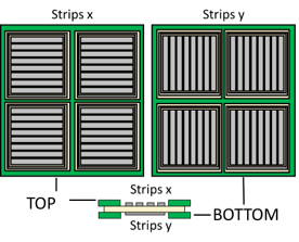
In this case, diamonds are used as solid-state ionization chambers: the motion of the charges generated by the particles hitting the diamond creates an instantaneous current that induces on the electrodes connected to the strips. This means that the detector can be modeled as a current source with both a capacitor and a resistor in parallel of each other. The resistor is neglected because it is so high to be considered (several TΩ) [3].
3 Front-end electronics design
We define a time measurement system as a FEE for radiation detectors that targets a time to digital converter (TDC) [4].
We focus on the input stage: the preamplifier, where we study the effect of its features on the final timing resolution. This latter is mathematically modeled as the maximum error of time defined using equation 3.1:
| (3.1) |
Where:
-
–
is linked to the resolution of the TDC which depends on its architecture;
-
–
is related to the discrimination stage and known as the time walk;
-
–
is usually associated to the noise of the preamplifier stage.
The represents the most critical element which we need to reduce to achieve high timing resolutions (). During this study, this error will be considered as the criteria of the time resolution.
3.1 The design methodology
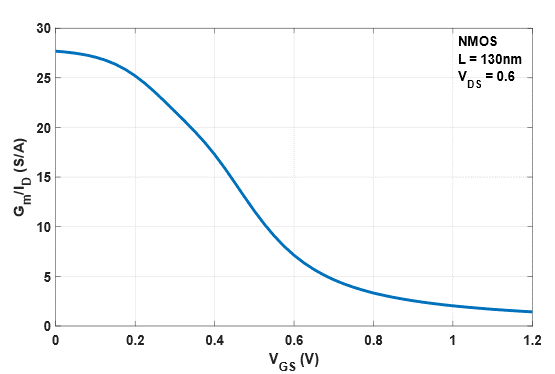
The design methodology allows to captures the relation between the fundamental function of the transistor (because fundamentally, a transistor is a voltage controlled current source), which is its transconductance and its power consumption . It was shown in [5] that the ratio is directly related to the most important analog specifications: speed, noise, efficiency, gain, swing and mismatch. Moreover, the range of values of is very limited, typically between 0 to 30. We illustrate its values after we extracted the LUTs of the used technology (130 nm CMOS technology)in figure 2. Also, it is important to know that this does not differs much from a device to another and from a technology to another [6].
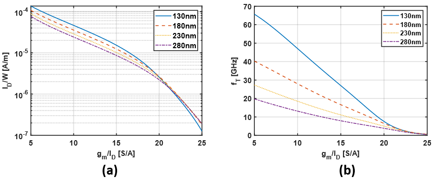
The use of the design methodology guarantee an efficient sizing of the transistors of the chosen topology, we apply it through a model-based design approach using MATLAB. In figure 3 (a) we can see that for the chosen technology (130nm CMOS), we can achieve a low power design while placing our transistors in a weak inversion mode. This ensures the lowest possible consumption. It illustrates as well (figure 3 (b)) that we keep a sufficient speed for such choice.
3.2 TIA topology
The proposed circuit is an 8 channels preamplifier-discriminator circuit based on a resistive feedback Transimpedance Amplifier (TIA) architecture shown in figure 4 (a) and a Leading-Edge Discriminator stage. For this TIA the gain is obtained directly from the feedback resistor. The use of the boost branch allows to minimize the current of the load of the main node and thus a higher open loop gain. The cascode helps to decrease the miller effect in order to preserve the targeted bandwidth.
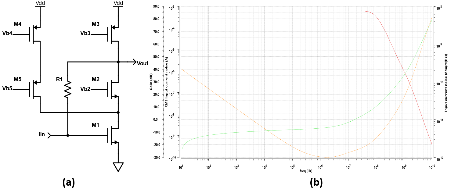
With this design, we achieve a DC gain of 87 dB and an UGF of 5 GHZ with an equivalent RMS current input noise of around 50nA as illustrated in figure 4 (b).
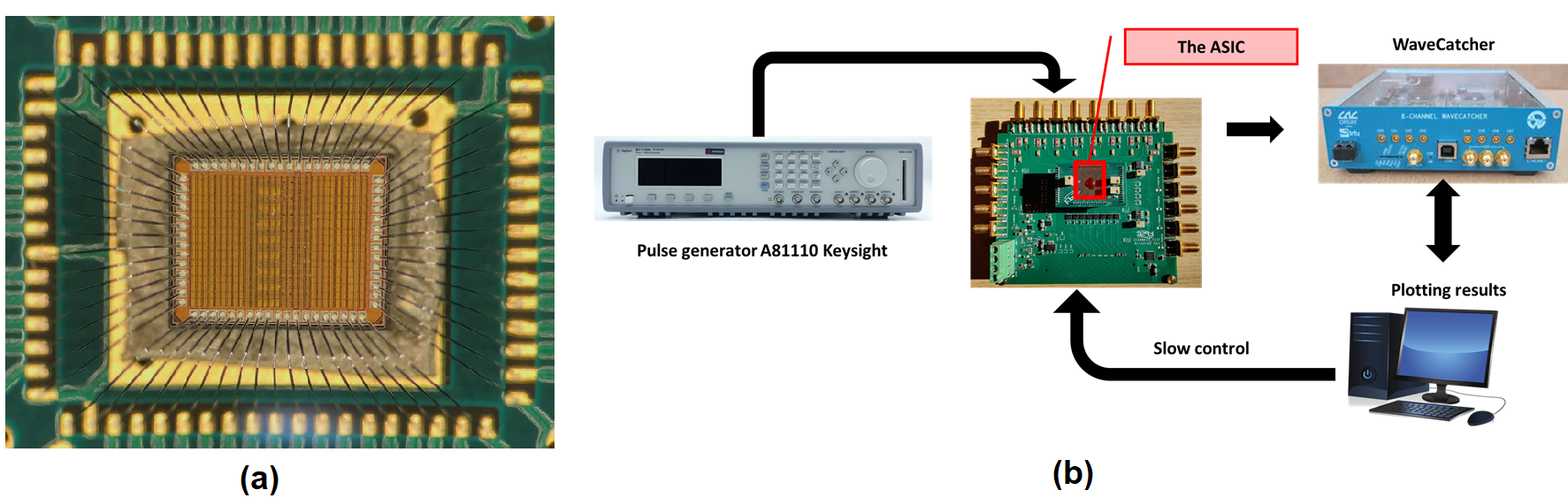
The circuit has been fabricated in a CMOS technology. The size of the chip is and the total power consumption of one channel is with a power supply of . Figure 5 (a) shows the fabricated circuit.
4 Test results
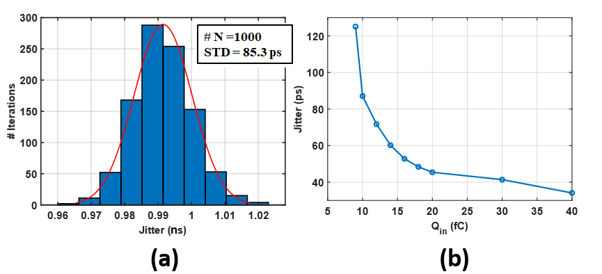
For the tests, the chip is mounted directly on a PCB (both input and output are bonded). This PCB is mounted on a test card where the supply and bias are applied. We emulate the behavior of the detector by injecting different values of charges through a capacitor of 1 pF using a precise pulse generator as shown in figure 5 (b). All the channels are activated. We record the values of the output for 1000 tests with every input in order to estimate as precisely as possible the timing jitter. Here we show the results in the case of an input charge of 10 fC, we achieve a timing jitter of around 85 ps. This value decreases for higher input charges as shown below.
5 Conclusion
In this paper, we discussed the design and testing results of an 8 channels preamplifier-discriminator circuit based on a resistive feedback Transimpedance Amplifier architecture and a Leading-Edge Discriminator stage for fast high-accuracy time measurement systems. The size of the chip is and the total power consumption of one channel is with a power supply of . Testing results shows a timing jitter of about for a input charge pulse.
References
- [1] Michal Pomorski. “Electronic properties of single crystal CVD diamond and its suitability for particle detection in hadron physics experiments." PhD thesis. Johann Wolfgang Goethe-Universität, 2008.
- [2] Yong Li et al., “Simulation method of charge collection mechanism in CVD diamond detector," 2016 PIERS. 10.1109/PIERS.2016.7734404
- [3] M. Fisher-Levine, et al., “A fast analogue front end for a diamond radiation spectrometer," IEEE Trans. Nucl. Sci., vol. 60, no. 5, pp. 3990–3994, Oct. 2013.
- [4] Abderrahmane GHIMOUZ et al., “A Preamplifier-discriminator circuit based on a Common Gate Feedforward TIA for fast time measurements using diamond detectors," 2018 25th IEEE ICECS, Bordeaux, France, 2018. 10.1109/ICECS.2018.8617950
- [5] Paul G. A. Jespers and Boris Murmann, “Systematic Design of Analog CMOS Circuits: Using Pre-Computed Lookup Tables," Cambridge University Press, 2017.
- [6] A. A. Youssef, B. Murmann and H. Omran, “Analog IC Design Using Precomputed Lookup Tables: Challenges and Solutions," in IEEE Access, vol. 8, pp. 134640-134652, 2020.