Date of publication xxxx 00, 0000, date of current version xxxx 00, 0000. 10.1109/ACCESS.2017.DOI
This work was partially funded by an U.S. Air Force STTR Phase I Contract awarded to Virtual EM Inc. (Contract No. FA9550-17-C-0001).
Corresponding author: Soumyajit Mandal (e-mail: soumya@alum.mit.edu).
A CMOS SoC for Wireless Ultrasonic Power/Data Transfer and SHM Measurements on Structures
Abstract
This paper describes a highly-integrated CMOS system-on-chip (SoC) for active structural health monitoring (SHM). The chip integrates ultrasonic power and bidirectional half-duplex data transfer, a power management unit (PMU), and an ultrasound transceiver to enable wireless ultrasonically-coupled sensor SHM networks on structures. The PMU includes an active bias-flip rectifier with off-delay compensation, high-efficiency dual-path DC-DC converter with inductor time-sharing, and five switched-capacitor DC-DC converters to generate multi-level spectrally band-limited pulses for guided-wave SHM. The chip was fabricated in a standard 180 nm process and has a die area of mm2. Test results show power conversion efficiency (PCE) for the active rectifier, % for the inductive DC-DC converter, and % for the switched-capacitor DC-DC converters. Output pulses have a peak-to-sidelobe ratio (PSL) dB and worst-case out-of-band emissions dB, respectively. The SoC was integrated with a low-power microcontroller and passive components to realize miniaturized (15 mm 30 mm) wireless SHM nodes. A set of nodes was deployed on an SHM test-bed (carbon fiber reinforced polymer sheet) representing an airframe panel. Tests on this wireless network confirm both long-range ultrasound power/data transfer and the ability to detect structural damage.
Index Terms:
Energy harvesting, structural health monitoring (SHM), ultrasound power/data transfer.=-15pt
I Introduction
Much of the world’s critical civil infrastructure, including bridges, pipelines, and transportation, is in increasingly poor condition due to the effects of ageing and deferred maintenance [1]. Structural health monitoring (SHM) is fast becoming an important component of any integrated strategy for managing the associated risks [2, 3, 4].
Broadly speaking, SHM sensors can be divided into two categories: passive (sensing-only) and active (both actuation and sensing). Scalable SHM systems of both types require small, lightweight, inexpensive, unobtrusive, and minimally invasive sensor networks [5]. Traditional wired SHM networks use individual wires for power and data transfer to each sensor node. The large number of wires required to support a large-scale wired network of this type presents installation and maintenance challenges. In addition, the weight of these wires is often unacceptable for high-value structures, such as airframes. Replacing point-to-point wired links with a single wired bus can reduce the weight of the wires, but introduces significant reliability challenges since a single-point bus failure can now disable the entire network. Using a RF-based wireless network can eliminate the wires [6], but at the expense of significantly higher power consumption (and hence lower operating lifetime). These networking issues are particularly challenging for active SHM nodes, which provide greater measurement flexibility (since actuation waveforms can be arbitrarily selected) but also have higher power consumption. Thus, while self-powered passive SHM nodes (typically using vibration energy harvesting) have been demonstrated [7, 8, 9], similar progress on wireless active SHM nodes is lacking.
These fundamental issues can be addressed by exploiting the high efficiency of directional ultrasound links for power/data transfer, as already demonstrated for biomedical implants [10, 11]. In fact, one can envision using guided acoustic waves propagating through the structure for both sensing and power/data transfer to the SHM nodes, thus enabling methods for jointly optimizing all three processes [12, 13]. We refer to such through-structure wireless networks for active SHM as being ultrasonically-coupled [14].
This paper describes the design and testing of a custom CMOS IC that enables miniaturized wireless sensor nodes for ultrasonically-coupled active SHM networks. Each autonomous node relies on this IC for wireless acoustic power and data transfer, power management, and making SHM measurements. The rest of this paper is organized as follows. Wireless SHM networks are introduced in Section II. The design of the IC is presented in Section III. Electrical characterization results from the IC are discussed in Section IV, while Section V presents measurement results obtained from an SHM test bed. Finally, Section VI concludes the paper.
II Introduction to Wireless SHM Networks
II-A SHM Measurements
Guided ultrasound waves are popular for SHM of thin-walled structures such as airframes, submarine hulls, storage tanks, and pipes. These “Lamb waves” can propagate relatively long distances with little loss, thus allowing a few sensors to monitor large areas of the structure using transmission (pitch-catch), reflection (pulse-echo), or passive (impact/acoustic emission detection) measurements [15, 16].
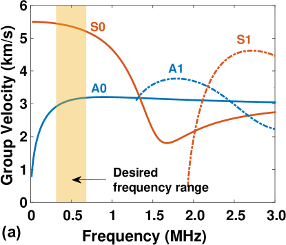
Multiple Lamb waves modes - either symmetric (denoted where ), or asymmetric (denoted ) - can propagate in thin-walled structures, as shown in Fig. 1(a). Moreover, the figure shows that they are generally dispersive, i.e., have frequency-dependent group velocities. To simplify subsequent signal processing and damage detection algorithms, most applications assume that only one or two wave modes (typically and ) have been excited. A band-limited excitation signal can be used for this purpose, as shown in the figure. Note that the required center frequency is material- and structure-dependent: it scales as where is the shear wave velocity in the material and is the thickness.
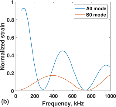
Thin piezoelectric transducers, which are also known as piezoelectric wafer active sensors (PWAS), are popular for generating and receiving Lamb waves due to their low profile, broadband characteristics, and low cost [17]. Their lateral (i.e., in-plane) vibrations excite Lamb wave modes in a frequency-dependent manner, as shown in Fig. 1(b). For example, in this case, operating around 300 kHz ensures that only the mode is excited. Thus, the spectral properties (center frequency, bandwidth, and side-lobe levels) of SHM transmitters must be precisely controlled to obtain the best monitoring results.
Both transmission- and reflection-type SHM measurements require pulsed waveforms to obtain spatial resolution. However, simple “on-off” pulses with rectangular amplitude profiles are undesirable because of their poor spectral side-lobe levels (worst-case of dB). Thus, windowed pulses should be used instead. For example, one can use cosine-sum or raised cosine window functions, which are defined as
| (1) |
where is a constant. The choice results in the Hamming window, which is favored for active SHM due its low worst-case side lobe level (approximately dB).
II-B Ultrasound Power Transfer on Structures
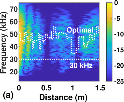
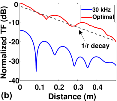
Guided ultrasound waves are also suitable for long-range wireless power and data transfer within structures [14]. The resulting ultrasound channels are highly frequency-selective due to multi-path propagation, which generates patterns of constructive and destructive interference (known as “slow fading”). For example, the measurements in Fig. 2(a) show complex frequency- and distance-dependent power transmission patterns even in a simple structure (a uniform metal plate). Fig. 2(b) shows that operating at the distance-dependent optimum frequency can significantly increase the available power (by dB in this case). Also, the available power decays slowly with distance (), as expected for guided waves in 2-D, thus enabling efficient long-distance power and (low-speed) data transfer. However, can change with time due to both environmental and structural changes (bending, temperature fluctuations, etc.). In earlier work, we addressed this challenge by developing a near-maximum power point tracking (nMPPT) algorithm that allows each node to track its own optimal transmission frequency [14].
II-C Ultrasonically-Coupled Network Architecture
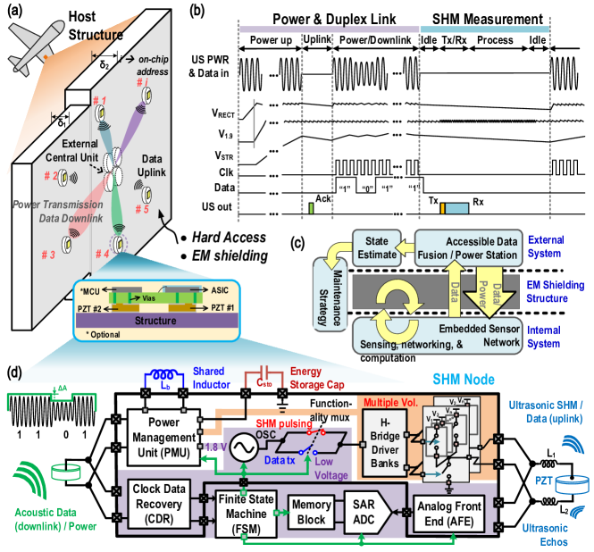
The overall design of a self-optimizing ultrasonically-coupled network for an emerging SHM application, namely monitoring hard-to-access areas of a structure, is shown in Fig. 3(a). A wired central unit (known as the hub) provides access to the external world. The hub delivers ultrasonic power to a distributed set of sensor nodes, and also maintains bidirectional data links with them. Each node contains a custom ASIC and microcontroller (MCU) for making local SHM measurements and transferring the results back to the hub for further processing. Fig. 3(b) shows important waveforms during a typical measurement cycle. During the first part of the cycle, nMPPT is used to find and enough power is delivered to power up the node. Next, the node sends an acknowledge (ACK) signal via the data uplink (node to hub). On receiving ACK, the hub sends instructions to the node via the data downlink (hub to node), for which bits are modulated on the power carrier. The node then uses these instructions to set its parameters (e.g., operating frequency, pulse length, etc.) and carries out either a transmission- or reflection-type SHM measurement. Finally, it uses the uplink to transmit acquired data back to the hub and returns to an idle (or sleep) state. The hub integrates data from multiple nodes to develop estimates of the current state of the structure (e.g., maps of stress distribution or damage locations). Such estimates can then be used by human operators and/or AI algorithms to drive maintenance decisions, as shown in Fig. 3(c).
III Chip Design
A highly-integrated ASIC is key for miniaturizing the proposed ultrasonically-coupled SHM sensor nodes (thus enabling deployment on non-planar surfaces) and also reducing their power consumption (thus enabling sparse sensor networks coupled via long-range links). Fig. 3(d) shows a block diagram of the proposed custom SHM IC, which is integrated together with an off-the-shelf ultra-low-power MCU to realize autonomous ultrasonically-coupled SHM sensor nodes. The chip is interfaced to two PWAS: the first (shown on the left) is used for acoustic power and data downlink from the central hub, while the second (shown on the right) is used for SHM measurements and also data uplink to the hub. Both links are designed to operate at programmable frequencies within the 100-500 kHz range to ensure single- or dual-mode Lamb wave propagation within a variety of structures (e.g., metal or carbon-fiber composite plates of different thicknesses).
The main components of the chip include the power management unit (PMU), clock and data recovery (CDR), SHM transmitter, load-shift keying (LSK)-based data transmitter, and the analog front-end (AFE) of the SHM receiver. The MCU contains the clock generator (which determines the operating frequency), a finite state machine (FSM) for sequencing the measurement, an ADC for digitizing the output of the SHM receiver, and on-chip memory (SRAM) for storing the results. In the next few sub-sections, we describe the major building blocks of the proposed IC in more detail.
III-A Active Rectifier
Power management is a major function of the proposed ultrasonically-coupled SHM IC. The first component of the PMU is an AC-DC converter (rectifier) that converts the AC voltage across transducer (i.e., PWAS) #1 into a DC voltage for recharging an energy storage capacitor. Fig. 4 shows the block diagram of the proposed rectifier. The core of the design is an active rectifier consisting of two PMOS switches (P1 and P2) and two NMOS switches (N1 and N2). The former are directly driven by the AC voltage across the transducer (), while the latter are driven by hysteretic push-pull comparators to minimize i) voltage drop during the ON period; and ii) reverse current flow during the OFF period. Each comparator internally generates an adaptive offset voltage to compensate for its own turn-OFF time delay, thus minimizing reverse current flow [18]. Note that only OFF-time delay compensation is implemented since reverse current directly degrades voltage and power conversion efficiency (VCE and PCE, respectively), while the ON-time delay only affects the conduction time of the switches.
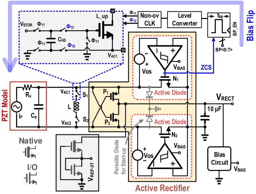
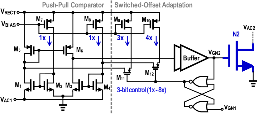
Fig. 5 shows one of the comparators in more detail. The design compares (or ) with ground to generate the gate control signal (or ). The input current mirrors M1-M4 are biased at nA (denoted in the figure) by , which is generated by a PTAT current reference as shown in Fig. 4. When goes low, it resets the SR latch, which turns on two offset currents (with nominal values of and ) that generate the required offset . The latch provides de-glitching and also ensures that the offset currents turn off when the complementary gate signal goes high. The optimal value of is load-dependent, and can be optimized via 3-bit control of the offset currents.
Since the comparators are powered by the rectified output , they are not available during “cold-start” conditions when the output capacitor is completely discharged. In this case, the parasitic drain-substrate diodes of and provide rectification (with lower efficiency), as shown in Fig. 4.
In a conventional full-bridge rectifier, each diode contributes a forward voltage drop V, such that the output DC voltage where is the amplitude of the AC voltage across the transducer. Moreover, the transducer has to charge its internal capacitance on every cycle, which wastes power. Fundamentally, this is because is out of phase with the transducer current due to the capacitive nature of the transducer impedance. The proposed rectifier uses “bias-flip” switches111This approach is also known as parallel-SSHI, where SSHI stands for “synchronized switch harvesting on inductor”. to improve the output power available from the transducer [19]. Specifically, switches and are placed in series with an off-chip shunt inductor and turned on when crosses zero. The inductive voltage then quickly flips the polarity of , which reduces the energy loss caused by charging/discharging . The resulting transducer voltage and current ( and ) are nearly in phase (resembling a resistive impedance), which maximizes the available power. A bootstrap driver (shown in the inset of Fig. 4) is used to create a floating gate-source voltage for controlling S1 and S2 through the AC cycle. During phase , the DC voltage on the storage capacitor () is stored on . During phase , the stored voltage is added to to set the gate voltage. The necessary switches use dynamic body biasing to ensure that their parasitic diodes remain OFF. Switch timing for the proposed bias-flip circuit is controlled by a feedback loop that digitally adjusts the pulse width (8-bit control) to ensure zero-current switching (ZCS).
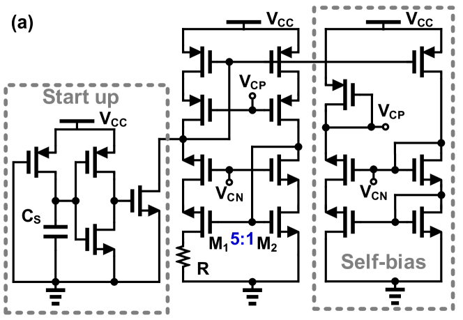
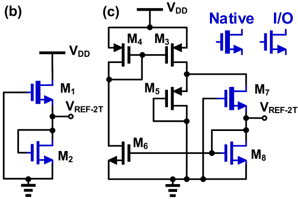
The unregulated output DC voltage is used to power two bias generator circuits. The first is a fully-cascoded constant- reference with a nominal output current of nA, shown in Fig. 6(a). The second uses a two-transistor (2T) reference [20] to generate a PVT-robust voltage. A basic 2T reference using native and I/O transistors is shown in Fig. 6(b). We modified this design to improve power supply regulation, as shown in Fig. 6(c). The reference current through M8 is mirrored to M6 and then M3 with a ratio , . The diode-connected device M5 then carries a current , ensuring that of M7 becomes nearly independent of . The output voltage mV, which is similar to the original design.
III-B DC-DC Converter
The DC-DC converter transforms the unregulated rectifier output into two regulated outputs: (nominally 3.3 V) and (nominally 2.0 V). The former is stored on a large energy reservoir (a super-capacitor in this case), while the latter powers the rest of the sensor node. Conventionally, these voltages are generated by two DC-DC converters in series, as shown in Fig. 7(a). The first converter ensures maximum power point tracking (MPPT) by adjusting its input impedance to ensure maximum power transfer from the rectifier (and ultimately the ultrasound transducer), while the latter regulates the load voltage . Unfortunately, this series configuration suffers from reduced power efficiency, since the PCE of the cascaded converters is the product of the individual efficiencies, i.e., .
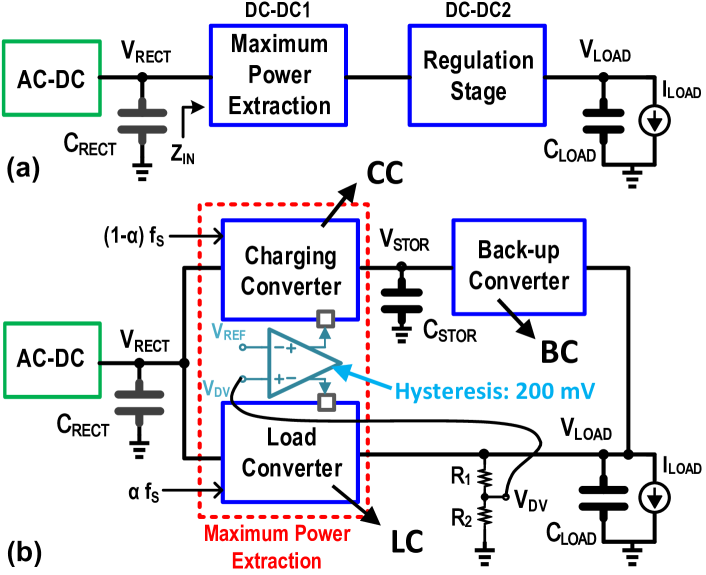
By contrast, here we propose a dual-path architecture [21] in which two boost converters - the charging converter (CC) and the load converter (LC) - are placed in parallel and adaptively selected by the current value of , as shown in Fig. 7(b). The LC delivers power to the load, while the CC allows excess power from the rectifier to be stored in for later use. In addition, a back-up buck converter (BC) is used to charge the load from if the latter requires more power than is currently available from the rectifier. The system can transition between these states on every switching cycle based on the current value of . For this purpose, several resistively-divided versions of (denoted by ) are compared with a reference voltage from the modified 2T circuit.
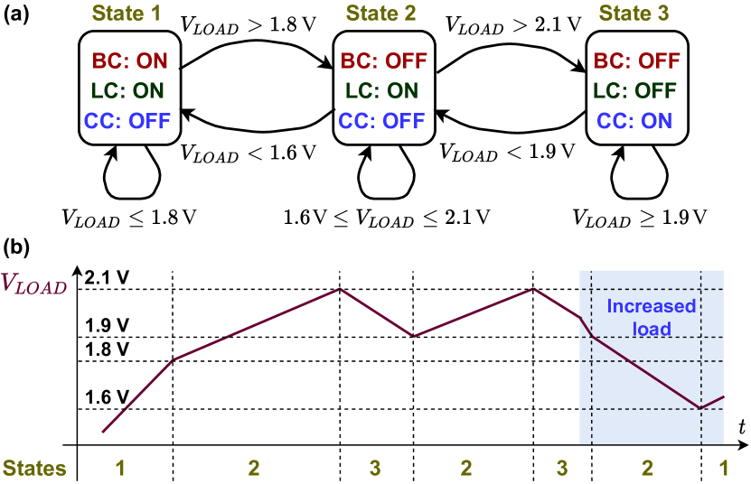
The resulting state transition diagram for the DC-DC converter can be summarized as shown in Fig. 8(a). Under normal conditions, the system cycles between states 2 and 3, resulting in a peak-to-peak ripple of mV around the nominal load voltage of 2.0 V as shown in Fig. 8(b); here is the amount of hysteresis between the switching thresholds for states 2 and 3 (2.1 V and 1.9 V, respectively). However, when the harvested power is insufficient for the load and drops below 1.6 V, the system transitions to state 1 (see Fig. 8(b)), where both the BC and LC are turned on to rapidly recharge . The switching thresholds for states 1 and 2 (1.8 V and 1.6 V, respectively) are also offset by mV. The resulting fluctuations in are acceptable for this application, but can be reduced by using a higher-resolution divider to set a smaller value for .
Let us denote the probability that the system is in state 2 by (). Clearly, the probability that the system is in either of the other two states is . Also, let us denote the PCE of the LC and CC (assumed to be equal for simplicity) as , and the PCE of the BC as . The PCE during state 2 is simply since only the LC is operating. On the other hand, states 1 and 3 together transfer energy to the load in two steps (), resulting in a effective PCE of . Thus, the average end-to-end PCE of the proposed DC-DC converter is given by
| (2) |
The availability of an upload data link (node to hub) allows the hub to regulate its output power level such that the harvested power is approximately equal to that consumed by the load. In this case the CC and BC are mostly inactive, i.e., . As a result, (2) simplifies to , which is likely to be significantly higher than the cascaded converter architecture. More generally, the system may receive more harvest more power than needed by the load, in which case it cycles between states 2 and 3 as described earlier. In this case, , such that and the effective duty cycles of the LC and CC are and , respectively.
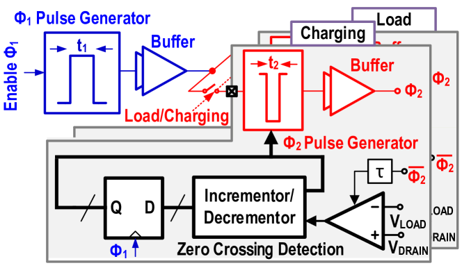
All three converters operate in discontinuous conduction mode (DCM), which allows them to use a single time-shared off-chip inductor . The input impedance (as seen by the rectifier) for a single boost converter can be found by estimating the average inductor current per cycle. Given the pulse widths and for the two switches (as controlled by the clock phases and , see Fig. 9(a)), the result is
| (3) | ||||
| (4) |
where is the switching frequency (fixed at 50 kHz in our design) and the approximation is valid when . Thus, can be controlled to adjust and thus ensure MPPT.
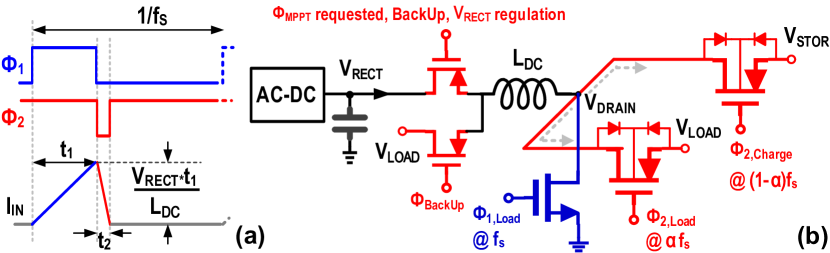
The switch configuration used for inductor time-sharing is shown in Fig. 9(b). There are a total of five switches: two series switches for the CC and LC, respectively; one shunt switch shared by them; one series switch for the BC; and one series switch for implementing both MPPT and rectifier under-voltage protection. Under normal circumstances when , either the LC or CC is always on (with duty cycles of and , respectively). As a result, the average value of is unchanged, which allows MPPT to be maintained:
| (5) |
Fig. 10 shows a simplified view of how the DC-DC architecture was implemented on-chip. Two feedback loops are used to adapt the switch timings, as shown by the green and blue arrows in Fig. 10. The green MPPT loop turns off the first series switch when the signal MPPT_SMP goes high, thus disconnecting the DC-DC converter from the rectifier. A sample-and-hold (S/H) within the “MPPT” block then measures the open-circuit voltage of the rectifier. Note that a hysteretic comparator also turns off this switch when the loaded rectifier voltage drops below a pre-set threshold, thus providing under-voltage protection. During normal operation, the loop ensures MPPT by adjusting the duration of (denoted by ), and thus , such that the loaded value of ; this is generally a good approximation to the maximum power point. Adjustment is performed digitally using an 6-bit accumulator, and can be disabled by a control signal MPPTEN as shown in Fig. 10.
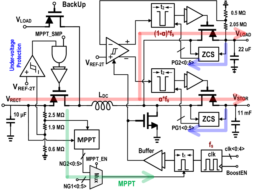
The second feedback mechanism consists of independent ZCS loops for the LC and CC. These blue loops are shown in more detail in Fig. 11. They use similar 6-bit digital control circuits to adjust the individual durations of (denoted by ) such that ZCS is obtained for the inductor current waveform, thus maximizing power efficiency. Finally, the present value of is used to switch between the LC and CC as described earlier, thus ensuring load voltage regulation.
III-C SHM Transmitter
Fig. 12 shows a block diagram of the transmitter (Tx) used for SHM measurements. The Tx generates pulses across PWAS #2 with shapes that approximate a Hamming-windowed tone burst, as shown in the figure. As described in Section II, windowing ensures that the pulse is localized in the frequency domain (i.e., does not have significant side-lobes), which improves the accuracy of SHM measurements by avoiding the excitation of multiple propagating Lamb wave modes. The earlier (wired) SHM transceiver IC described in [22] used pulse-width modulation (PWM) to generate a close approximation to a Hamming-windowed pulse. However, PWM requires the use of a high-frequency clock (in the earlier design, higher than the operating frequency) to generate narrow pulses, which significantly increases overall power consumption of the IC. The new design eliminates this problem by dynamically switching between multiple power supply voltages during the pulse, thus directly controlling its amplitude on a cycle-by-cycle basis. The cycle period, and thus the center frequency of the pulse, is externally programmable via the clock frequency, resulting in a dB excitation bandwidth of for a five-cycle pulse, where the factor of arises from the Hamming window.
The transmitter circuit uses a H-bridge topology to ensure high power-efficiency and maximize the output signal swing (up to ), as shown in Fig. 12. Small off-chip inductors and are placed in series with the load (i.e., the ultrasound transducer) to create a series circuit with quality factor , which suppresses harmonics and further boosts the steady-state voltage across the transducer by a factor of up to . The high-side PMOS switches of the H-bridge are split into five pairs (–). Each pair is supplied by a different DC supply voltage (denoted –), thus enabling the pulse envelope to be dynamically controlled using the switching sequence shown in the figure, which is generated on-chip from a single external trigger pulse. The necessary DC voltages are generated by on-chip switched-capacitor DC-DC converters, as described next.
III-D Switched-Capacitor DC-DC Converters
A set of five parallel switched-capacitor converters use pulse-frequency modulation (PFM) [23] to efficiently generate the five regulated output voltages required by the transmitter, namely V, V, V, V, and V. These values were obtained by numerical optimization, with the target being the best possible five-level approximation to the desired SHM transmit pulse waveform (five cycles long, Hamming-windowed). Simulations show that the five-level pulse has 20 dB lower worst-case sidelobe level than a simple “on-off” tone burst, resulting in a peak-to-sidelobe ratio (PSL) of approximately dB.
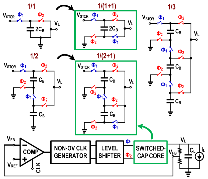
Three of the five required DC levels were generated by 1/1 ratio converters: i) V 3.3 V and 2.87 V; and ii) V 1.9 V. The two remaining voltage levels were obtained as follows: i) a 1/3 ratio converter to generate 0.89 V from , and ii) a 1/2 ratio converter to generate 0.36 V from 0.89 V. The necessary switched-capacitor configurations are shown in Fig. 13. The 1/1 converters consist of a single switch between the input ( in the figure) and output (), and are not shown for simplicity. For the 1/2 and 1/3 converters, we used the configurations highlighted in Fig. 13 (“1/(1+1)”and “1/(2+1)”, respectively) rather than the alternative designs also shown in the figure, which require more switches and thus have lower efficiency. The “1/(1+1)”and “1/(2+1)” configurations can be derived from basic 1/1 and 1/2 converter designs by adding a single pair of switches, as indicated by the arrows.
A similar PFM-based voltage-regulation loop is used for each converter, as shown in Fig. 13. The loop feeds back a divided version of the output voltage (denoted by ) to a hysteretic comparator, which then enables/disables the local non-overlapping clock generator. A relatively low value of hysteresis (50 mV) was used to ensure low output voltage ripple, and thus accurately-shaped pulses. The on-chip capacitance used by the 1/2 and 1/3 converters was set to a relatively large value ( pF) to ensure low output impedance. Finally, voltage droop during the pulse was minimized by using off-chip capacitors ( nF) to store enough charge at each output node.
III-E Transmit-Receive Switch
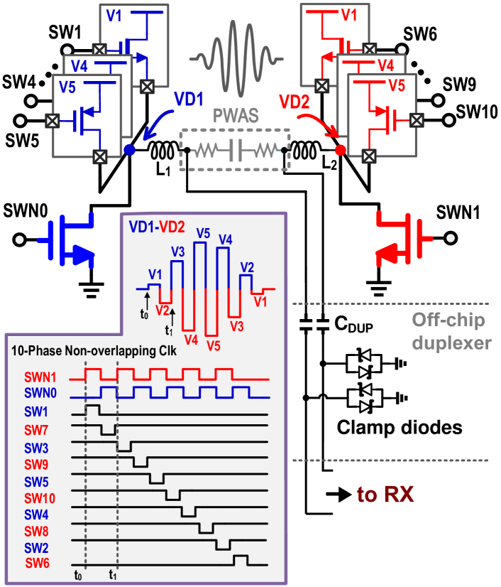
Since the PWAS voltage can significantly exceed (due to the voltage amplification provided by the resonant load), a simple off-chip transmit-receive switch (duplexer) was used to protect the input terminals of the SHM receiver. This circuit consists of small series capacitors and two sets of back-to-back diode clamps, as shown in Fig. 12. In transmit mode, the diodes turn on (behaving as a short circuit), thus placing an effective capacitance in parallel with the PWAS and limiting the voltage across the receiver terminals to one diode drop (approximately V). The value of is chosen to be significantly smaller than the transducer capacitance to ensure that the added capacitance does not significantly degrade transmitter efficiency. In receive mode, the diodes turn off (behaving as an open circuit), thus allowing the received signals to pass into the receiver through .
III-F Receiver
The receiver design is shown in Fig. 14. The first stage is a fully-differential low-noise amplifier (LNA) based on a folded-cascode OTA topology. The gain of the LNA is set by capacitive feedback to ; here is digitally programmable via a 4-bit capacitor DAC. The presence of causes the gain to decrease to where , thus degrading the input-referred noise from its design value of 10 nV/Hz1/2. To minimize such degradation, we set . Thus, the condition is required for the proposed passive duplexer to work as intended. In our design pF and pF, so we used pF to approximate , which is a suitable value. Note that we have ignored the off-state capacitance of the diodes (which further attenuates the received signal) for simplicity; low-capacitance diodes ( pF) were used to minimize additional signal attenuation.
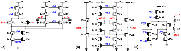
The rest of the receiver uses a standard super-heterodyne topology with fully-differential signal path to minimize even-order distortion and common-mode noise. Quadrature down-conversion (using passive double-balanced mixers) is used to down-convert received SHM signals to baseband, thus minimizing the sampling rate required by the MCU’s ADC. The LNA output is buffered by a fully-differential folded-cascode op-amp (shown in Fig. 15) before driving the mixers. The op-amp uses a nominal bias current of A derived from a 1 A constant- reference. The latter also generates the other op-amp bias voltages (–). A continuous-time CMFB loop is used for simplicity, as shown in Fig. 15(c).
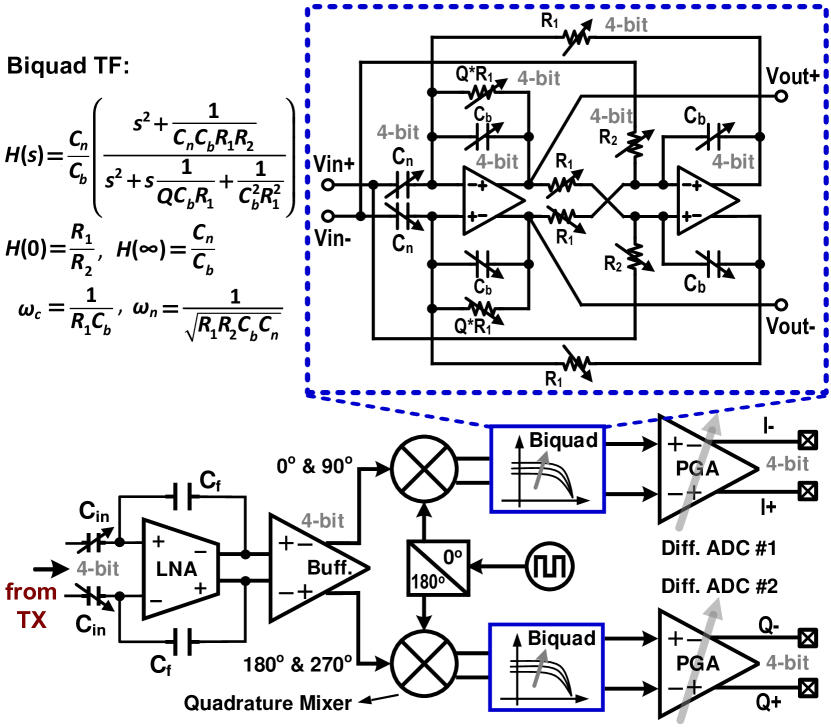
The quadrature outputs ( and ) of the mixer are low-pass filtered by a second-order biquad [24] (shown as an inset in Fig. 14) before being amplified by a differential programmable-gain amplifier (PGA). Both the biquad and the PGA use the same op-amp as in the mixer buffer. The biquad transfer function (TF) is shown in the figure. It has a Chebyshev-type response with programmable DC gain (), stop-band rejection (), cut-off frequency (), and notch frequency (). We fixed and programmed the other biquad parameters (and thus the frequency response of the receiver) using 4-bit resistor and capacitor DACs interfaced to a standard 3-wire on-chip SPI port. The goal is to match the excitation bandwidth of while minimizing out-of-band noise and clock feedthrough.
III-G Ultrasound Data Transceiver
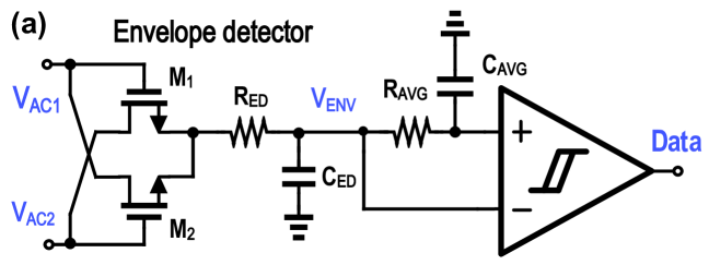
The ultrasonic downlink and uplink reuse the two PWAS used for power delivery and SHM measurements (#1 and #2, respectively), as shown in Fig. 3(d). The hub uses binary frequency shift keying (BFSK) to modulate downlink data on the power carrier. The strongly frequency-selective ultrasound channel converts such frequency modulation into amplitude modulation, as indicated on the figure. The on-chip clock and data recovery (CDR) block uses an envelope detector (ED) and hysteretic comparator to extract the amplitude-modulated bits, as shown in Fig. 16(a). Typical SHM measurement cycles are slow ( measurement/hour), so relatively low downlink data rates (10-200 bits/sec) are generally used.
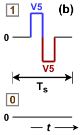
Uplink data is transmitted on PWAS #2 by reusing the SHM transmitter shown in Fig. 12. For this purpose, the switches connected to voltages – (– and –) are disabled, with only and (connected to V) remaining active. Thus, the transmitter output reduces to a single-cycle pulse, as shown in Fig. 16(b). Data is encoded using on-off keying (OOK) to minimize energy consumption: the presence of a pulse within a symbol period represents ‘1’, while its absence represents ‘0’.
IV Electrical Characterization Results
IV-A SHM Node Design
The SHM chip was designed in the TSMC 180 nm standard CMOS process and fabricated through Muse Semiconductor. Fig. 17(a) shows a labeled die photograph of the IC, which measures 2 mm 2 mm. All on-chip bias voltages and currents were internally generated using on-chip constant- current references and 2T-type voltage references.
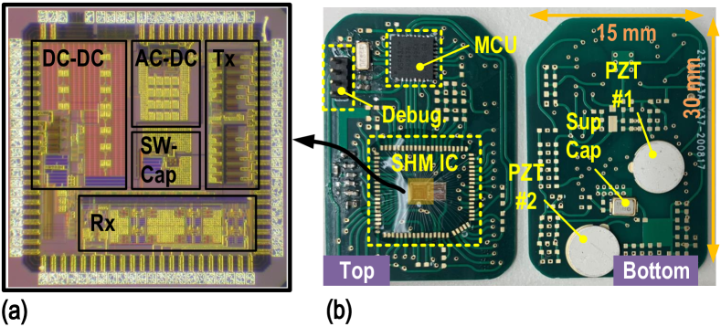
The custom SoC was integrated with an off-the-shelf ultra-low-power MCU (MSP430FR2476, Texas Instruments), two low-profile lead zirconate titanate (PZT) ultrasound transducers (diameter of 5 mm), and passive components (including F, F, and mF) to realize miniaturized and fully-autonomous wireless SHM sensor nodes, as shown in Fig. 17(b). Bare dies were assembled using a chip-on-board method to minimize node size (currently, 15 mm 30 mm). This section describes electrical test results from the sensor node, while the next section presents SHM results from a test-bed.
IV-B Active Rectifier
Fig. 18 shows the experimental setup used for measuring the VCE and PCE of the active rectifier. The input AC voltage and current were monitored using two differential probes, with the second connected across a 120 sense resistor. The output DC voltage at various loads was monitored using a Keithley source meter unit (SMU).

Fig. 19 shows measured results from the proposed rectifier. Figs. 19(a) and (b) show the PCE and VCR, respectively, as a function of input frequency for three different values of load resistance (). Both PCE and VCR decrease with frequency due to increased dynamic loss in the switches and comparators. Also, PCE decreases with increased load (i.e., lower values of ) at low frequencies due to increased conduction loss in the switches, but the trend is reversed at high frequencies where dynamic loss (which is largely load-independent) is dominant. Excellent performance (PCE %, VCR %) is obtained over the expected operating range ( k, kHz).
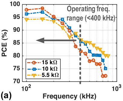
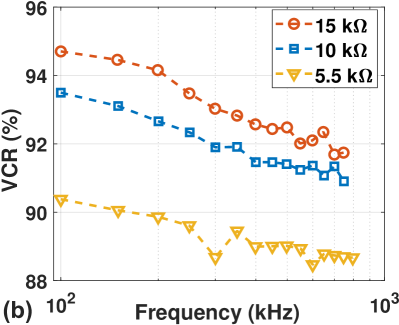
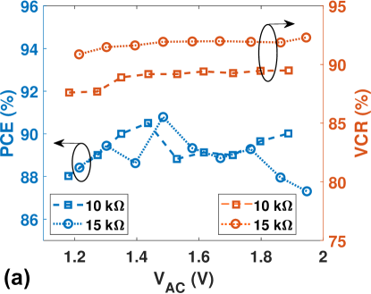
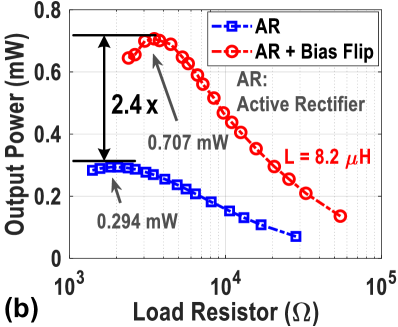
Fig. 20(a) shows that the measured PCE and VCR are nearly independent of AC input amplitude over the typical operating range ( V) at kHz. This result again suggests that conduction loss (which decreases with ) is small compared to dynamic loss. Fig. 20(b) shows the output power as a function of in two cases: i) using the active rectifier (AR) alone, and ii) combining the AR with a small off-chip inductor ( H) and the bias-flip circuit. The latter increases the maximum available power by 2.4, as expected.
IV-C DC-DC Converter
Typical measured waveforms for the DC-DC converter are shown in Fig. 21. The central figure shows a zoomed-out view, highlighting the switching frequency of kHz. The zoomed-in views on the left and the right show cases where the CC and the LC are ON, respectively. As expected, the voltage of the common drain node () equals when the CC is ON, while it equals when the LC is ON. After either converter turns off, the parasitic capacitance at (which is now floating) results in high-frequency ringing. However, this does not affect the regulated voltages.
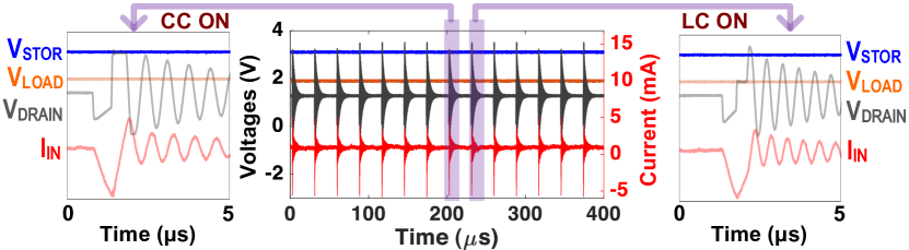
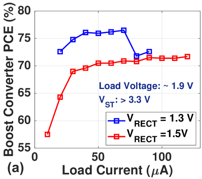
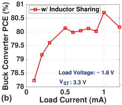
Fig. 22 summarizes the measured PCE of the DC-DC converter versus load current. Fig. 22(a) shows the PCE for the time-shared boost converters (CC and LC) under normal conditions, with the system cycling between states 2 and 3 such that . The figure shows that PCE % is maintained over the typical range of for load currents A. Fig. 22(b) shows the PCE for the back-up buck converter (BC), which is only active in state 1. In this case, PCE % is maintained over a wide range of load currents.
IV-D Switched-Capacitor DC-DC Converters
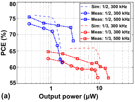
Fig. 23(a) compares measured and simulated PCE of the 1/2 and 1/3 ratio switched-capacitor (SC) DC-DC converters (used by the SHM transmitter) versus output power for various conversion ratios and clock frequencies . PCE improves with , as expected; this is because the output resistance of a SC converter is a strongly-decreasing function of switching frequency. In particular, theoretical models predict when is relatively low (known as the slow-switching limit) [25]. In addition, the measured PCE is slightly higher than the simulations, probably due to higher-than-expected switching losses due to parasitic capacitance. The 1/1 converters do not contribute significantly to power loss since they use a single switch, which results in significantly higher PCE; thus, their performance is not shown here.
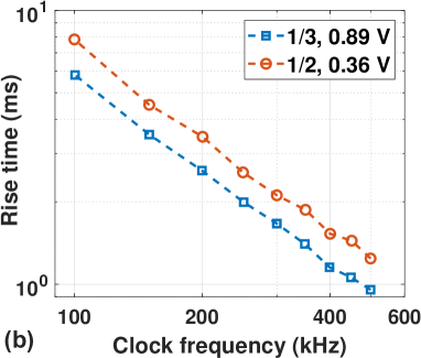
Fig. 23(b) plots the rise time of the 1/2 and 1/3 converters versus . The figure shows that rise time is inversely proportional to , which suggests that in agreement with theoretical models.
IV-E SHM Transmitter
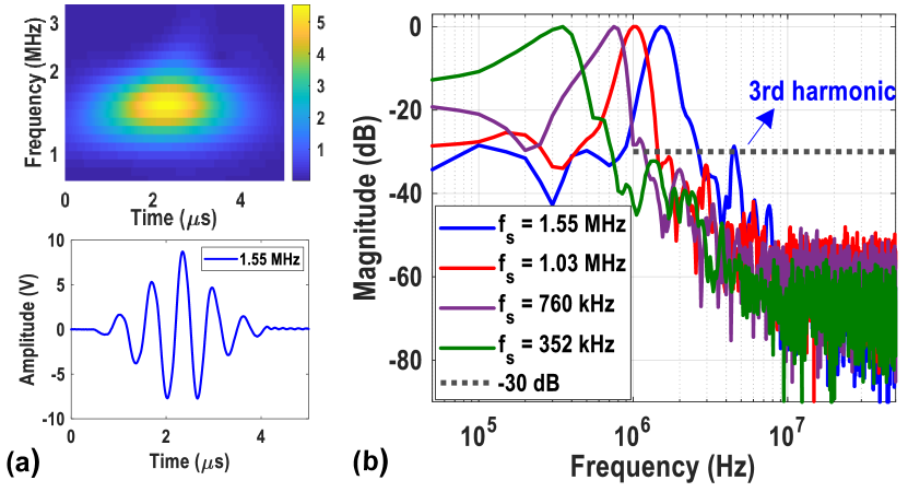
Fig. 24 shows electrical test results for the SHM transmitter. Fig. 24(a) shows a typical output pulse across the transducer in the time-frequency plane (top) and the time-domain (bottom). The waveform closely resembles a Hamming-windowed tone burst, as desired. Note that passive amplification by the tuned load significantly increases the peak voltage amplitude compared to that generated by the chip ( V).
The resulting frequency spectra (at different operating frequencies) are shown in Fig. 24(b). In each case, the off-chip series inductors ( and ) were adjusted to match the desired operating frequency. The smooth envelope of the pulse strongly suppresses side-bands; the worst-case PSL is 30 dB, in agreement with simulations. Similarly, the tuned circuit suppresses harmonics, with worst-case out-of-band emissions (caused by the third harmonic) being smaller than dBc.
IV-F SHM Receiver
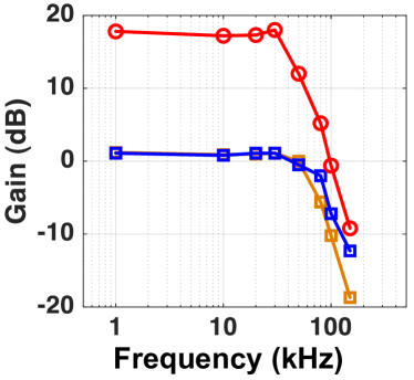
Fig. 25(a) shows measured small-signal transfer functions for the receiver at different gain and bandwidth settings; these results are in good agreement with simulations. The maximum available dB bandwidth is 100 kHz, which is adequate over the desired range of center frequencies for SHM measurements ( kHz) given that the excitation bandwidth is . Similarly, the maximum gain of 20 dB is adequate for SHM applications, where received signal amplitudes of 10-100 mV are typical in both transmission and reflection mode.
IV-G Performance Summary and Comparison
Table I compares the performance of this chip with other SHM ICs in the literature, including our own earlier work [22, 26]. This work achieves excellent spectral localization of the transmit waveform by suppressing both sidelobes and harmonics. It is also the first to integrate ultrasonic power and data transfer capabilities within the chip, thus enabling ultrasonically-coupled SHM sensor nodes.
| Parameter | This Work | CICC 2018 [22] | NEWCAS 2016 [26] | JSSC 2014 [27] |
|---|---|---|---|---|
| Technology | 0.18 m CMOS | 0.5 m CMOS | 0.5 m CMOS | 0.25 m BCD |
| Number of Tx | 1 | 1 | 1 | 4 |
| Number of Rx | 1 | 1 | 1 | – |
| Tx Windowing Performance | 36 dB (2nd harmonic) | dB | – | dB |
| Tx Output (Maximum) | 16 V | 6.3 V | 15 V | 36 V |
| Tx Frequency Range | 0.05-2.5 MHz | 0.1-2.2 MHz | 0.55-1 MHz | 780 kHz |
| Remotely-Powered | Yes | No | No | No |
| Communications | Ultrasound half-duplex | I2C | No | No |
| Tx Power Consumption | 13.2 J / 5 s TX | 875 W | 325-575 W | 28 J / s TX |
| Die Size | mm2 | mm2 | mm2 | mm2 |
V Active SHM measurements
The functionality of the chip was verified by carrying out SHM measurements out on a test-bed representing an airframe panel. For this purpose, a set of wireless sensor nodes (#1–#6) was attached on one side of a carbon fiber reinforced polymer (CFRP) sheet (0.3 m 0.3 m, 2 mm thick).
V-A Power Transfer
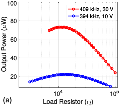
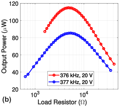
Using the bias-flip circuit, a peak output power of 75 W was obtained at a distance of 17 cm (from node #3 to node #4) for a transmit amplitude of 30 V at the optimal excitation frequency of kHz, as shown in Fig. 27(a). Similar measurements for a slightly shorter link (distance 12 cm, from node #2 to node #5) and closely-spaced excitation frequencies ( kHz and 377 kHz) are shown in Fig. 27(b) for a transmit amplitude of 20 V. These results show that available power decreases significantly (by 25%) when increases by only 1 kHz from its optimum value, which highlights the frequency-selective nature of the acoustic channel and the need to adaptively set for each node using nMPPT methods. It is also interesting to note that available power levels are significantly lower (by about ) than earlier experiments over similar distances using thin aluminum plates [14], either because of worse acoustic impedance matching with the PZT transducers or the anisotropic mechanical properties of the CFRP sheet.
V-B Data Transfer
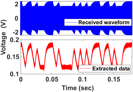
Fig. 27 shows typical downlink data transmission waveforms at 200 bits/sec and a distance of 10 cm (from node #7 to node #3). The frequency-selective ultrasound channel converts the BFSK-modulated waveform generated by the hub (node #7) into amplitude shift-keying (ASK), as expected. The measured bit error rate (BER) is (no bit errors were detected within bits). Finally, OOK-based uplink data transmission with BER was achieved for distances up to 20 cm and rates up to 10 kbits/s.
V-C Localization of Structural Damage
A variety of damage detection and localization algorithms have been proposed for SHM using guided ultrasound waves [16, 28, 29]. The general approach relies on comparing the current observation with one or more previous baselines recorded from undamaged structures, thus generating differential features that quantify changes from the baselines. These features generally include time-varying changes in the baselines due to environmental fluctuations (e.g., in temperature), which must be removed using various compensation methods [30]. Finally, anomalies are detected when the compensated differential features exceed certain predefined threshold values.
A set of 6 wireless sensor nodes were used for initial damage localization experiments on the SHM test-bed. For this purpose, a drop of water was placed on the surface of the CFRP sheet to locally perturb the Lamb wave velocity and thus simulate structural damage, as shown in Fig. 28(a). Data for a single measurement was acquired by transmitting from one node and receiving from all the nodes. The process was then repeated with each of the 6 sensor nodes serving as the transmitter, thus resulting in a data matrix.
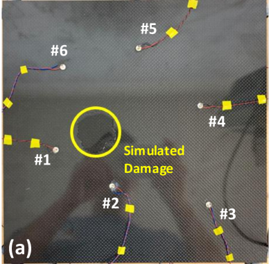
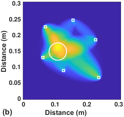
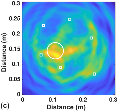
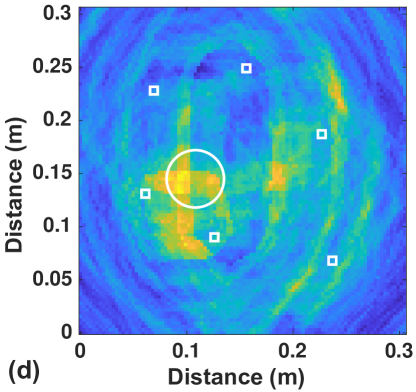

Data matrices obtained with and without the simulated damage were then processed off-line using two well-known SHM algorithms, namely RAPID (Reconstruction Algorithm for Probabilistic Inspection of Damage) [28] and delay-and-sum (DAS) [31], to extract damage localization maps. The resulting maps, which are shown in Figs. 28(b)-(c), encode the probability that damage is present at each spatial point on the test-bed. The results show that both RAPID and DAS algorithms can successfully localize the simulated damage. However, the RAPID algorithm relies on combining pairwise measurements and thus has poor sensitivity to points outside the convex hull of sensor node positions, which reduces its usefulness for large-area SHM. While the DAS algorithm does not suffer from this problem, a close examination of the resulting damage map (Fig. 28(c)) shows relatively poor spatial resolution and several unwanted maxima outside the damage region. These issues can be addressed by using a more accurate Lamb wave propagation model. Due to the anisotropic mechanical properties of the CFRP sheet, the group velocity acquires a non-uniform angular dependence that affects the DAS results. This dependence was experimentally characterized for the test-bed by using pair-wise propagation measurements and then included in the DAS algorithm. The resulting group velocity compensated damage map is shown in Fig. 28(d); it has significantly improved spatial resolution, as expected.
VI Conclusion
This paper has described a highly-integrated SoC that enables ultrasonically-coupled wireless SHM networks on structures. Electrical test results confirm the functionality of all major on-chip blocks, including the PMU, SHM transceiver, and ultrasound data transceiver. The chip was used to realize autonomous sensor nodes that were successfully deployed on an SHM test-bed (CFRP panel). Future work will focus on further miniaturization of the sensor nodes by integrating a two-channel ADC, clock generator, FSM, and SRAM on the chip, thus eliminating the external MCU.
Acknowledgment
The authors would like to thank Prof. Joel Harley for insightful discussions, and Mohammed Sameer Shaik for assistance with the experiments.
References
- [1] J. W. Hall, M. Tran, A. J. Hickford, and R. J. Nicholls, The future of national infrastructure: A system-of-systems approach. Cambridge University Press, 2016.
- [2] J. M. Brownjohn, “Structural health monitoring of civil infrastructure,” Philosophical Transactions of the Royal Society A: Mathematical, Physical and Engineering Sciences, vol. 365, no. 1851, pp. 589–622, 2007.
- [3] A. Raghavan and C. E. Cesnik, “Review of guided-wave structural health monitoring,” The Shock and Vibration Digest, vol. 39, no. 2, pp. 91–114, 2007.
- [4] C. R. Farrar and K. Worden, “An introduction to structural health monitoring,” Philosophical Transactions of the Royal Society A: Mathematical, Physical and Engineering Sciences, vol. 365, no. 1851, pp. 303–315, 2006.
- [5] Y. Hu, W. S. Rieutort-Louis, J. Sanz-Robinson, L. Huang, B. Glišic, J. C. Sturm, S. Wagner, and N. Verma, “Large-scale sensing system combining large-area electronics and CMOS ICs for structural-health monitoring,” IEEE Journal of Solid-State Circuits, vol. 49, no. 2, pp. 513–523, 2014.
- [6] E. Sazonov, K. Janoyan, and R. Jha, “Wireless intelligent sensor network for autonomous structural health monitoring,” in Smart Structures and Materials 2004: Smart Sensor Technology and Measurement Systems, vol. 5384. International Society for Optics and Photonics, 2004, pp. 305–314.
- [7] Y. Lee, D. Blaauw, and D. Sylvester, “Ultralow power circuit design for wireless sensor nodes for structural health monitoring,” Proceedings of the IEEE, vol. 104, no. 8, pp. 1529–1546, 2016.
- [8] C. Huang and S. Chakrabartty, “An asynchronous analog self-powered CMOS sensor-data-logger with a 13.56 MHz RF programming interface,” IEEE Journal of Solid-State Circuits, vol. 47, no. 2, pp. 476–489, 2011.
- [9] H. Salehi, S. Das, S. Chakrabartty, S. Biswas, and R. Burgueño, “Damage identification in aircraft structures with self-powered sensing technology: A machine learning approach,” Structural Control and Health Monitoring, vol. 25, no. 12, p. e2262, 2018.
- [10] D. Seo, R. M. Neely, K. Shen, U. Singhal, E. Alon, J. M. Rabaey, J. M. Carmena, and M. M. Maharbiz, “Wireless recording in the peripheral nervous system with ultrasonic neural dust,” Neuron, vol. 91, no. 3, pp. 529–539, 2016.
- [11] J. Charthad, M. J. Weber, T. C. Chang, and A. Arbabian, “A mm-sized implantable medical device (IMD) with ultrasonic power transfer and a hybrid bi-directional data link,” IEEE Journal of Solid-State Circuits, vol. 50, no. 8, pp. 1741–1753, 2015.
- [12] X. Li, C. You, S. Andreev, Y. Gong, and K. Huang, “Wirelessly powered crowd sensing: Joint power transfer, sensing, compression, and transmission,” IEEE Journal on Selected Areas in Communications, vol. 37, no. 2, pp. 391–406, 2018.
- [13] M. Mälzer, C. Kexel, T. Maetz, and J. Moll, “Combined inspection and data communication network for Lamb-wave structural health monitoring,” IEEE transactions on ultrasonics, ferroelectrics, and frequency control, vol. 66, no. 10, pp. 1625–1633, 2019.
- [14] S. M. Shaik, X. Tang, and S. Mandal, “Self-optimizing wireless networks on structures,” IEEE Transactions on Circuits and Systems II: Express Briefs, vol. 67, no. 5, pp. 911–915, 2020.
- [15] Z. Su, L. Ye, and Y. Lu, “Guided Lamb waves for identification of damage in composite structures: A review,” Journal of Sound and Vibration, vol. 295, no. 3-5, pp. 753–780, 2006.
- [16] V. Giurgiutiu, Structural health monitoring: with piezoelectric wafer active sensors. Elsevier, 2007.
- [17] ——, “Lamb wave generation with piezoelectric wafer active sensors for structural health monitoring,” in Smart Structures and Materials 2003: Smart Structures and Integrated Systems, vol. 5056. International Society for Optics and Photonics, 2003, pp. 111–122.
- [18] R. Erfani, F. Marefat, S. Nag, and P. Mohseni, “A 1–10-MHz frequency-aware CMOS active rectifier with dual-loop adaptive delay compensation and -mW output power for capacitively powered biomedical implants,” IEEE Journal of Solid-State Circuits, vol. 55, no. 3, pp. 756–766, 2019.
- [19] Y. K. Ramadass and A. P. Chandrakasan, “An efficient piezoelectric energy harvesting interface circuit using a bias-flip rectifier and shared inductor,” IEEE Journal of Solid-State Circuits, vol. 45, no. 1, pp. 189–204, 2009.
- [20] M. Seok, G. Kim, D. Blaauw, and D. Sylvester, “A portable 2-transistor picowatt temperature-compensated voltage reference operating at 0.5 V,” IEEE Journal of Solid-State Circuits, vol. 47, no. 10, pp. 2534–2545, 2012.
- [21] S. Bandyopadhyay and A. P. Chandrakasan, “Platform architecture for solar, thermal, and vibration energy combining with MPPT and single inductor,” IEEE Journal of Solid-State Circuits, vol. 47, no. 9, pp. 2199–2215, 2012.
- [22] X. Tang, H. Zhao, and S. Mandal, “A programmable CMOS transceiver for structural health monitoring,” in 2018 IEEE Custom Integrated Circuits Conference (CICC). IEEE, 2018, pp. 1–4.
- [23] J. Kwong, Y. K. Ramadass, N. Verma, and A. P. Chandrakasan, “A 65 nm sub- microcontroller with integrated SRAM and switched capacitor DC-DC converter,” IEEE Journal of Solid-State Circuits, vol. 44, no. 1, pp. 115–126, 2008.
- [24] H. Shin and Y. Kim, “A CMOS active-RC low-pass filter with simultaneously tunable high- and low-cutoff frequencies for IEEE 802.22 applications,” IEEE Transactions on Circuits and Systems II: Express Briefs, vol. 57, no. 2, pp. 85–89, 2010.
- [25] M. D. Seeman and S. R. Sanders, “Analysis and optimization of switched-capacitor DC–DC converters,” IEEE Transactions on Power Electronics, vol. 23, no. 2, pp. 841–851, 2008.
- [26] H. Zamani, C. Chen, X. Tang, P. Mohseni, and S. Mandal, “A current-controlled transceiver IC for structural health monitoring,” in 2016 14th IEEE International New Circuits and Systems Conference (NEWCAS). IEEE, 2016, pp. 1–4.
- [27] Y. Guo, C. Aquino, D. Zhang, and B. Murmann, “A four-channel, 36 V, 780 kHz piezo driver chip for structural health monitoring,” IEEE Journal of Solid-State Circuits, vol. 49, no. 7, pp. 1506–1513, 2014.
- [28] X. Zhao, H. Gao, G. Zhang, B. Ayhan, F. Yan, C. Kwan, and J. L. Rose, “Active health monitoring of an aircraft wing with embedded piezoelectric sensor/actuator network: I. Defect detection, localization and growth monitoring,” Smart materials and structures, vol. 16, no. 4, p. 1208, 2007.
- [29] J. E. Michaels, “Detection, localization and characterization of damage in plates with an in situ array of spatially distributed ultrasonic sensors,” Smart Materials and Structures, vol. 17, no. 3, p. 035035, 2008.
- [30] A. J. Croxford, J. Moll, P. D. Wilcox, and J. E. Michaels, “Efficient temperature compensation strategies for guided wave structural health monitoring,” Ultrasonics, vol. 50, no. 4-5, pp. 517–528, 2010.
- [31] X. Tang, J. B. Harley, K. Bi, T. Ozdemir, M. B. Pawloski, and S. Mandal, “Sparse sensor networks for active structural health monitoring using highly integrated CMOS transceivers,” in Sensors and Smart Structures Technologies for Civil, Mechanical, and Aerospace Systems 2018, vol. 10598. International Society for Optics and Photonics, 2018, p. 105983H.