Fermi level tuning and double-dome superconductivity in the kagome metals CsV3Sb5-xSnx
Abstract
The recently reported AV3Sb5 (A = K, Rb, Cs) family of kagome metals are candidates for unconventional superconductivity and chiral charge density wave (CDW) order; both potentially arise from nested saddle points in their band structures close to the Fermi energy. Here we use chemical substitution to introduce holes into CsV3Sb5 and unveil an unconventional coupling of the CDW and superconducting states. Specifically, we generate a phase diagram for CsV3Sb5-xSnx that illustrates the impact of hole-doping the system and lifting the nearest vHs toward and above . Superconductivity exhibits a non-monotonic evolution with the introduction of holes, resulting in two “domes” peaked at 3.6 K and 4.1 K and the rapid suppression of three-dimensional CDW order. The evolution of CDW and superconducting order is compared with the evolution of the electronic band structure of CsV3Sb5-xSnx, where the complete suppression of superconductivity seemingly coincides with an electron-like band comprised of Sb orbitals pushed above EF.
Kagome metals naturally support electronic structures that host Dirac points, flat bands, and saddle points, leading to electronic instabilities associated with divergences in the density of states at the Fermi level. A wide array of instabilities have been predicted, ranging from bond density wave order [1, 2] to charge fractionalization [3, 4], charge density waves (CDW) [5], and superconductivity (SC) [1, 6]. As a result, the interplay between competing electronic instabilities can often be tuned via small changes in the band filling. For example, band fillings near electrons per band [1, 7, 8, 9, 10] can populate nested van Hove singularities (vHs) that drive CDW order, and, in some limits, unconventional superconductivity.
The recently discovered class of AV3Sb5 (A: K, Rb, Cs) kagome metals [11] are potential realizations of this physical mechanism with each member exhibiting experimental signatures associated with CDW order [12, 13, 14, 15, 16, 17] followed by the low temperature onset and coexistence of superconductivity [14, 15, 18]. Upon applying hydrostatic pressure, the CDW instability in AV3Sb5 is coupled to superconductivity in a seemingly unconventional fashion [19, 20], and the impact of the pressure-modified band structure on the interplay between the two states remains an open area of study. In particular, understanding the relative roles of the vHs comprised of V -orbital states near the -points and the electron-like band comprised of Sb-states at the -point within the CDW and SC mechanisms is essential to developing a microscopic picture of how the two transitions are coupled.
Carrier doping is an appealing means of tuning these features relative to the Fermi level and probing the coupling of the CDW and SC states. Shifting the relative positions of the vHs and pocket relative to and probing the evolution and interplay of the CDW and SC phase transitions can provide insights into the origins of each state. A recent study on oxidized thin flakes of CsV3Sb5, for instance, shows that hole-doping on the Cs site can enhance while also suppressing CDW order [21]. In addition, DFT calculations show that hole-doping drives the vHs in the opposite direction relative to EF than that expected via external hydrostatic pressure [22]. Given that an unusual coupling between SC and CDW states was observed under variable pressure [20], a systematic study of hole-doping effects stands to provide an important experimental window into understanding this unconventional coupling.
Here the effect of hole-doping on the CDW and SC states in CsV3Sb5-xSnx with 0 1.5 is presented. Hole-doping is achieved via substitution of Sn onto the Sb sites, and, because Sn and Sb are very similar in size, this drives negligible coincident steric effects in the band structure. As holes are introduced, the CDW state is rapidly suppressed, and three-dimensional CDW order vanishes near = 0.06. In parallel, SC is enhanced and reaches a maximum =3.6 K at = 0.03 within the CDW state before decreasing as the CDW is fully suppressed. Continued hole-doping beyond the suppression of CDW order results in a second maximum in =4.1 K at = 0.35 prior to bulk SC weakening and vanishing beyond = 0.5. Density functional theory (DFT) calculations and nuclear quadrupolar resonance measurements establish a strong preference for Sn to occupy Sb sites within the kagome plane, and DFT models predict that Sn substitution on this site lifts the Sb electron-like band at above EF coincident with the vanishing of bulk SC. Furthermore, only small changes in the energies of the vHs are predicted for doping levels sufficient to suppress signatures of CDW order, suggesting the importance of Sb-states in the stabilization of both phases.
Powder samples of CsV3Sb5-xSnx for 0 1 in 6–7 g batches were synthesized using a combination of ball milling and high-temperature sintering [23]. Structural analysis was performed via synchrotron powder x-ray data acquired at Argonne National Laboratory (APS, 11-BM) and on a Panalytical Empyrean laboratory x-ray powder diffractometer. A Hitachi TM4000Plus scanning electron microscope (SEM) was used to perform energy–dispersive x-ray spectroscopy (EDS). Magnetization data were collected in a Quantum Design Magnetic Property Measurement System (MPMS) and electrical resistivity data were collected in a Quantum Design Physical Property Measurement System (PPMS). DFT calculations were performed within the Vienna ab initio Simulation Package (VASP) [24, 25], and room temperature 121Sb zero-field NQR measurements were performed using a custom NMR spectrometer. Further details are available in the Supplemental Material accompanying this manuscript [23].
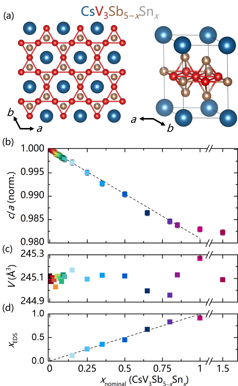
At room temperature, CsV3Sb5-xSnx with 0 1 all adopt the same hexagonal structure as CsV3Sb5 with an ideal kagome network of V atoms, shown in Fig. 1(a). For 0 1, polycrystalline samples were found to be single phase, while a secondary phase appears for = 1.5, indicating the termination of the solid solution. Pawley fits of powder diffraction data were used to determine changes to the unit cell as a function of Sn content. Figures 1(b-c) show the normalized ratio and the cell volume as a function of Sn content. With increasing Sn, increases and decreases in near perfect compensation, yielding a cell volume which is virtually independent of Sn content. Small fluctuations in volume of less than 0.16% can be explained by uncertainties in chemical composition and in the structural refinement.
The linear trend in is reminiscent of a Vegard’s Law-type trend, suggesting that Sn is incorporated into the parent structure as a solid solution up to approximately = 1, at which point the ratio plateaus. Figure 1(d) indicates that the measured Sn content (via EDS) tracks the nominal Sn content. While Rietveld refinements of x-ray data confirm that powders are single phase, poor scattering contrast between Sb and Sn impedes the ability to refine whether Sn is uniformly distributed on both the Sb1 and Sb2 sites, or whether there is preferential occupation of a particular sublattice. DFT calculations suggest a preference 10 meV/atom for Sn to substitute preferentially on the Sb1 (in the kagome plane) and nuclear quadropole resonance (NQR) measurements (discussed later) confirm that Sn atoms preferentially occupy this site [23].
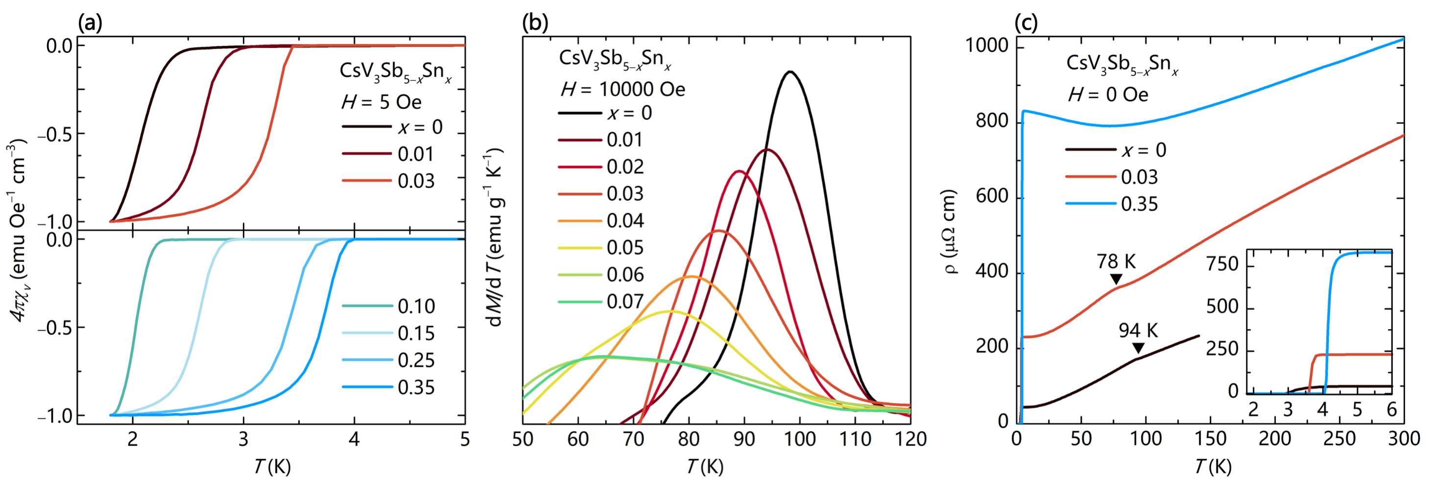
Undoped CsV3Sb5 single crystals have a superconducting =2.5 K [14, 21] and a charge density wave transition temperature =94 K [13, 16] that drives a structural distortion into a enlarged unit cell; one containing layers of kagome nets distorted into both star-of-David and tri-hexagonal structures [26, 13, hu2022coexistence]. Polycrystalline samples show identical transition temperatures, although both transitions are broader compared to single crystals [14]. This is largely due to powders being very sensitive to exact synthesis conditions and strain effects [23]. Pure CsV3Sb5 powder synthesized here has an onset of 2.70 K and a midpoint of 2.07 K. As Sn is added within the matrix, Figure 2(a) shows the evolution of superconductivity, focusing on two different doping regimes ( = 0 to 0.03 and = 0.1 to 0.35). All superconducting samples show in magnetization. Fractions slightly exceeding unity are attributed to errors in the packing density, and data are normalized to for ease of comparison. The effect of Sn on becomes immediately apparent: as the Sn content is increased to = 0.03, increases to a local maxima of 3.6 K. then decreases with continued hole-doping, followed by a second superconducting dome appearing shortly thereafter with a maximum = 4.1 K at x=0.35. Superconductivity assumes only a partial volume fraction for 0.5, and the SC state completely disappears by = 0.85. An exhaustive set of susceptibility measurements is provided in the supplemental information [23].
The evolution of CDW order upon hole-doping can be monitored via via the inflection point in magnetization that appears at the CDW onset. Using the peak in d/d as a metric for the onset of three-dimensional CDW order, Fig. 2(b) shows that light hole substitution causes the CDW transition to rapidly broaden and shift to lower temperatures. Undoped, the peak in d/d is 98.01 K and this peak decreases to less than 80 K at x=0.04. For 0.05, signatures of the CDW transition in magnetization cannot be resolved, although it is possible that a highly broadened CDW anomaly smoothly continues its rapid suppression with higher Sn doping. Despite the ambiguity in the precise position of CDW phase boundary near =0.05, the superconducting and CDW states clearly coexist at the first maximum of the first superconducting dome ( = 0.03). This is distinct from the second maximum in at higher Sn content ( = 0.35), which occurs far beyond the apparent suppression of CDW order. Future work studying single crystals will be required to fully map if the suppression of the CDW state is a first or second order phase boundary and to fully explore whether CDW order is becoming short-ranged at larger Sn-doping levels.
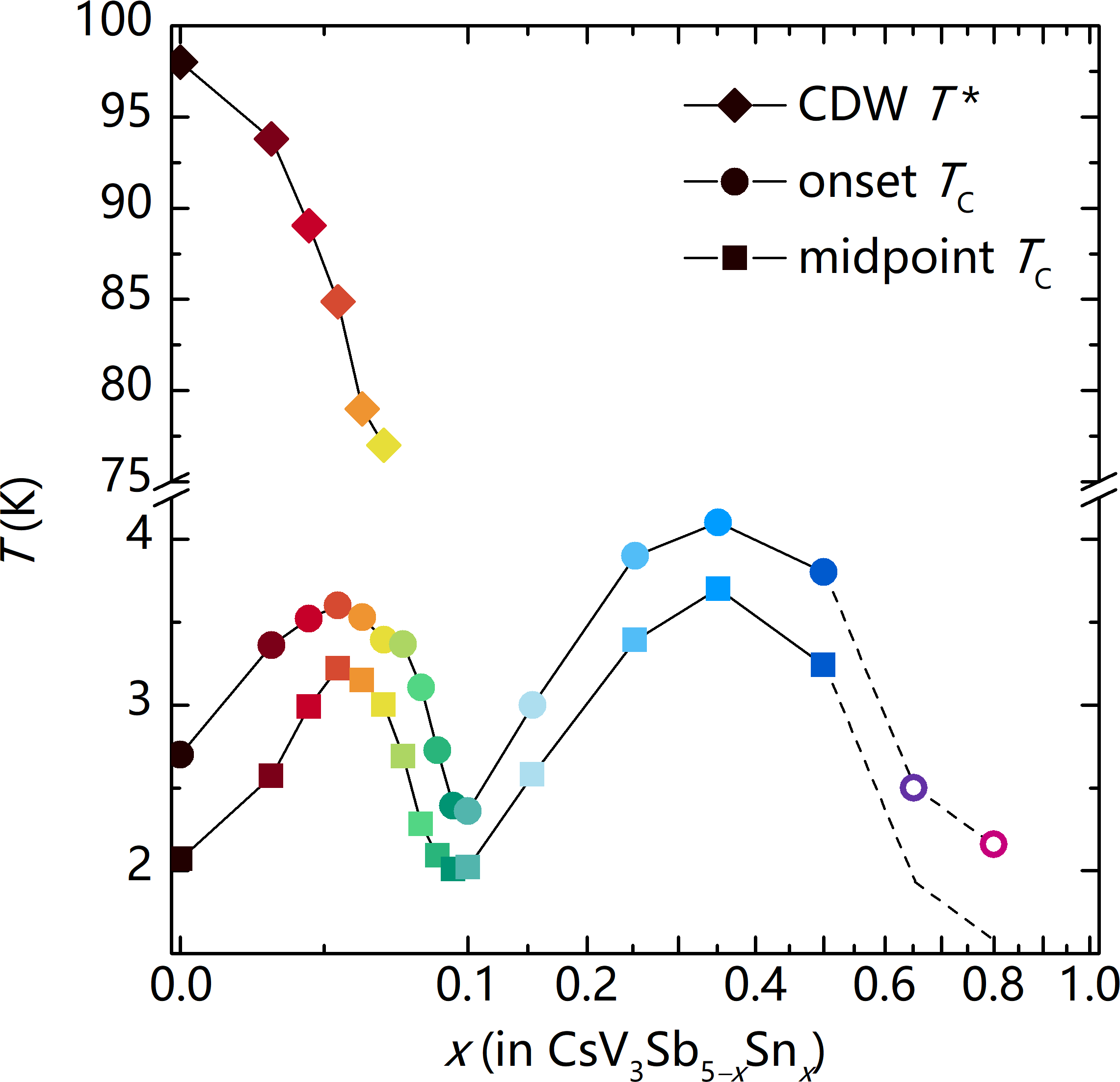
Figure 2(c) shows electrical resistivity measurements performed on samples at both peak values (0.03 and 0.35). Zero-resistivity conditions agree well with the obtained via magnetization measurements, and the CDW onset temperature is further marked for the sample with = 0.03. The resistance immediately prior to the onset of SC increases quite dramatically upon Sn substitution, from 50 -cm ( = 0), to 250 -cm ( = 0.03, first peak), to 800 -cm ( = 0.35, second peak), and the temperature dependence of the resistivity, particularly near the CDW temperature, changes dramatically with Sn doping. As a summary, Figure 3 plots a phase diagram showing the effect of Sn-substitution on both SC and CDW orders. A two-dome structure is immediately evident in , as is the relatively rapid suppression of CDW order with the introduction of Sn.
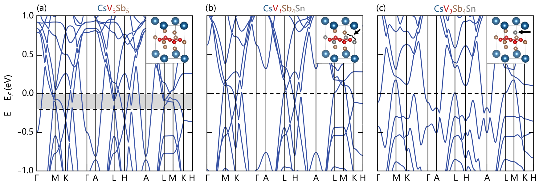
The CsV3Sb5 lattice supports nearly 1/5 of the total Sb being replaced by Sn. To give a rough sense of the range over which can be tuned, Figure 4(a) shows the electronic structure of pure CsV3Sb5 along with the range of Fermi levels achievable with a loss of 1 electron per unit cell (gray shaded region). In a rigid band shift approximation, substitution of Sn should allow to be tuned across multiple vHs and Dirac points near the - and -points, respectively. However, reconstruction of the bands associated with the Sb orbitals and orbital selective doping effects are expected, and Figure 4(c) shows one hypothetical structure with Sn substituted on the Sb2 sublattice (out of the kagome plane). Here, in addition to the expected shift of the Fermi level (note the position of the -point vHs crossing now 0.2 eV above ), a significant reconstruction is also resolved around the K, L, and H points. Notably, the electron-like band at is preserved in this structure. Alternatively, if Sn substitution instead occupies the Sb1 sublattice within the kagome plane, the overall electronic structure relative to CsV3Sb5 is largely preserved and mimics a rigid band shift model, with the important exception of the Sb-derived -pocket, which vanishes and is replaced with an electron-like Sn-band far above . Colorized orbital contributions to the band structure structures shown in Fig. 4 are presented in the supplemental information [23].
To clarify the impact of Sn-doping on the band structure, NQR measurements were performed and establish that Sn preferentially occupies the Sb1 sites in the kagome plane [23]. This is consistent with DFT calculations that show a small energy preference for Sn occupying the Sb1 site. With this doping-site established, supercell calculations at fractional in-plane Sb substitution were performed and show that, as Sn content is increased, the electron-like band at lifts above near = 0.5 in tandem with the disappearance of bulk superconductivity [23]. This suggests that superconductivity in CsV3Sb5 in-part relies on the Sb -derived orbitals, and aligns with results of earlier pressure studies [27].
At smaller Sn-doping levels, the observation of an intermediate peak in demonstrates a complex interplay between the Sb-states at and the V -states driving the CDW order. Supercell calculations show a rather mild shift in the -point vHs from roughly 0.072 eV below for =0 to 0.047 eV for =0.33 and 0.042 eV for =0.5, prior to shifting 0.083 eV above in =1. The small shift in the expected energies of the vHs toward under mild =0.05 substitution fails to explain the rapid suppression of the CDW state at this doping, suggesting a complicated balance of energy scales underpinning the CDW state. This is consistent with the rapid suppression of the CDW state under hydrostatic pressure [19, 20]; however the two SC domes apparent under hole-doping seem distinct from those realized under pressure. Superconductivity in crystals nominally doped between the SC domes retains a sharp transition [23], unlike the weak SC observed in pressure studies. Further work exploring the distinctions between pressure (pushing vHs away from ) and hole-doping (pulling vHs toward ) is required to fully explore the parallels between the hole-doping and pressure-driven phase diagrams.
Hole-doping realized via chemical substitution of Sn into CsV3Sb5 results in a complex electronic phase diagram featuring two SC domes – one that coexists with CDW order and a second that appears following the suppression of the CDW state. Unconventional superconductivity has been predicted for fillings slightly away from the vHs [8]. The enhancement of prior to the suppression of CDW order and the subsequent second peak in following the complete suppression of the CDW state motivate deeper theoretical studies into how the Sb states intertwine with both CDW order SC in these materials. Our results demonstrate that small changes in the electronic structure achieved through carrier doping can have dramatic impacts on SC and CDW orders in CsV3Sb5 and provide a elegant chemical means to tune the competition between these states in the new AV3Sb5 class of kagome superconductors.
I acknowledgments
This work was supported by the National Science Foundation (NSF) through Enabling Quantum Leap: Convergent Accelerated Discovery Foundries for Quantum Materials Science, Engineering and Information (Q-AMASE-i): Quantum Foundry at UC Santa Barbara (DMR-1906325). The research reported here made use of shared facilities of the NSF Materials Research Science and Engineering Center at UC Santa Barbara DMR-1720256, a member of the Materials Research Facilities Network (www.mrfn.org). Use of the Advanced Photon Source at Argonne National Laboratory was supported by the U.S. Department of Energy, Office of Science, Office of Basic Energy Sciences, under Contract No. DE-AC02-06CH11357. YMO is supported by the National Science Foundation Graduate Research Fellowship Program under Grant No. DGE-1650114. BRO is supported by the California NanoSystems Institute through the Elings Fellowship program. FK acknowledges the Roy T. Eddleman Center for Quantum Innovation (ECQI) for their support. Work at Brown was supported in part by the the National Science Foundation grant No. DMR-1905532 and funds from Brown and University of Bologna.
References
References
- Wang et al. [2013] W.-S. Wang, Z.-Z. Li, Y.-Y. Xiang, and Q.-H. Wang, Competing electronic orders on kagome lattices at van Hove filling, Phys. Rev. B 87, 115135 (2013).
- Isakov et al. [2006] S. V. Isakov, S. Wessel, R. G. Melko, K. Sengupta, and Y. B. Kim, Hard-core bosons on the kagome lattice: Valence-bond solids and their quantum melting, Phys. Rev. Lett. 97, 147202 (2006).
- O’Brien et al. [2010] A. O’Brien, F. Pollmann, and P. Fulde, Strongly correlated fermions on a kagome lattice, Phys. Rev. B 81, 235115 (2010).
- Rüegg and Fiete [2011] A. Rüegg and G. A. Fiete, Fractionally charged topological point defects on the kagome lattice, Phys. Rev. B 83, 165118 (2011).
- Guo and Franz [2009] H.-M. Guo and M. Franz, Topological insulator on the kagome lattice, Phys. Rev. B 80, 113102 (2009).
- Ko et al. [2009] W.-H. Ko, P. A. Lee, and X.-G. Wen, Doped kagome system as exotic superconductor, Phys. Rev. B 79, 214502 (2009).
- Yu and Li [2012] S.-L. Yu and J.-X. Li, Chiral superconducting phase and chiral spin-density-wave phase in a Hubbard model on the kagome lattice, Phys. Rev. B 85, 144402 (2012).
- Kiesel et al. [2013] M. L. Kiesel, C. Platt, and R. Thomale, Unconventional Fermi surface instabilities in the kagome Hubbard model, Phys. Rev. Lett. 110, 126405 (2013).
- Barros et al. [2014] K. Barros, J. W. Venderbos, G.-W. Chern, and C. Batista, Exotic magnetic orderings in the kagome Kondo-lattice model, Phys. Rev. B 90, 245119 (2014).
- Feng et al. [2021] X. Feng, K. Jiang, Z. Wang, and J. Hu, Chiral flux phase in the Kagome superconductor AV3Sb5, Sci. Bull. (2021).
- Ortiz et al. [2019] B. R. Ortiz, L. C. Gomes, J. R. Morey, M. Winiarski, M. Bordelon, J. S. Mangum, I. W. Oswald, J. A. Rodriguez-Rivera, J. R. Neilson, S. D. Wilson, et al., New kagome prototype materials: discovery of KV3Sb5, RbV3Sb5, and CsV3Sb5, Phys. Rev. Mater. 3, 094407 (2019).
- Jiang et al. [2021] Y.-X. Jiang, J.-X. Yin, M. M. Denner, N. Shumiya, B. R. Ortiz, G. Xu, Z. Guguchia, J. He, M. S. Hossain, X. Liu, et al., Unconventional chiral charge order in kagome superconductor KV3Sb5, Nat. Mater. , 1 (2021).
- Zhao et al. [2021] H. Zhao, H. Li, B. R. Ortiz, S. M. Teicher, T. Park, M. Ye, Z. Wang, L. Balents, S. D. Wilson, and I. Zeljkovic, Cascade of correlated electron states in a kagome superconductor CsV3Sb5, arXiv preprint arXiv:2103.03118 (2021).
- Ortiz et al. [2020] B. R. Ortiz, S. M. Teicher, Y. Hu, J. L. Zuo, P. M. Sarte, E. C. Schueller, A. M. Abeykoon, M. J. Krogstad, S. Rosenkranz, R. Osborn, R. Seshadri, L. Balents, J. He, and S. D. Wilson, CsV3Sb5: A topological kagome metal with a superconducting ground state, Phys. Rev, Lett. 125, 247002 (2020).
- Ortiz et al. [2021a] B. R. Ortiz, P. M. Sarte, E. M. Kenney, M. J. Graf, S. M. Teicher, R. Seshadri, and S. D. Wilson, Superconductivity in the kagome metal KV3Sb5, Phys. Rev. Mater. 5, 034801 (2021a).
- Liang et al. [2021] Z. Liang, X. Hou, W. Ma, F. Zhang, P. Wu, Z. Zhang, F. Yu, J.-J. Ying, K. Jiang, L. Shan, et al., Three-dimensional charge density wave and robust zero-bias conductance peak inside the superconducting vortex core of a kagome superconductor CsV3Sb5, arXiv preprint arXiv:2103.04760 (2021).
- Chen et al. [2021a] H. Chen, H. Yang, B. Hu, Z. Zhao, J. Yuan, Y. Xing, G. Qian, Z. Huang, G. Li, Y. Ye, et al., Roton pair density wave and unconventional strong-coupling superconductivity in a topological kagome metal, arXiv preprint arXiv:2103.09188 (2021a).
- Yin et al. [2021] Q. Yin, Z. Tu, C. Gong, Y. Fu, S. Yan, and H. Lei, Superconductivity and normal-state properties of kagome metal RbV3Sb5 single crystals, Chinese Phys. Lett. 38, 037403 (2021).
- Du et al. [2021] F. Du, S. Luo, B. R. Ortiz, Y. Chen, W. Duan, D. Zhang, X. Lu, S. D. Wilson, Y. Song, and H. Yuan, Pressure-induced double superconducting domes and charge instability in the kagome metal KV3Sb5, Phys. Rev. B 103, L220504 (2021).
- Chen et al. [2021b] K. Chen, N. Wang, Q. Yin, Y. Gu, K. Jiang, Z. Tu, C. Gong, Y. Uwatoko, J. Sun, H. Lei, et al., Double superconducting dome and triple enhancement of in the kagome superconductor CsV3Sb5 under high pressure, Phys. Rev. Lett. 126, 247001 (2021b).
- Song et al. [2021] Y. Song, T. Ying, X. Chen, X. Han, Y. Huang, X. Wu, A. P. Schnyder, J.-G. Guo, and X. Chen, Enhancement of superconductivity in hole-doped CsV3Sb5 thin films, arXiv preprint arXiv:2105.09898 (2021).
- LaBollita and Botana [2021] H. LaBollita and A. S. Botana, Tuning the van Hove singularities in AV3Sb5 (= K, Rb, Cs) via pressure and doping, arXiv preprint arXiv:2108.04876 (2021).
- [23] See Supplemental Information for further details.
- Kresse and Furthmüller [1996a] G. Kresse and J. Furthmüller, Efficient iterative schemes for ab initio total-energy calculations using a plane-wave basis set, Phys. Rev. B 54, 11169 (1996a).
- Kresse and Furthmüller [1996b] G. Kresse and J. Furthmüller, Efficiency of ab-initio total energy calculations for metals and semiconductors using a plane-wave basis set, Comput. Mater. Sci. 6, 15 (1996b).
- Ortiz et al. [2021b] B. R. Ortiz, S. M. Teicher, L. Kautzsch, P. M. Sarte, J. P. Ruff, R. Seshadri, and S. D. Wilson, Fermi surface mapping and the nature of charge density wave order in the kagome superconductor CsV3Sb5, arXiv preprint arXiv:2104.07230 (2021b).
- Tsirlin et al. [2021] A. A. Tsirlin, P. Fertey, B. R. Ortiz, B. Klis, V. Merkl, M. Dressel, S. D. Wilson, and E. Uykur, Anisotropic compression and role of Sb in the superconducting kagome metal CsV3Sb5, arXiv preprint arXiv:2105.01397 (2021).