Dynamical Study of the Origin of the Charge Density Wave
in V3Sb5 (K, Rb, Cs) Compounds
Abstract
Systems containing the ideal kagome lattice can exhibit several distinct and novel exotic states of matter. One example of such systems is a recently discovered V3Sb5 ( = K, Rb, and Cs) family of compounds. Here, the coexistence of the charge density wave (CDW) and superconductivity is observed. In this paper, we study the dynamic properties of the V3Sb5 systems in context of origin of the CDW phase. We show and discuss the structural phase transition from to symmetry that are induced by the presence of phonon soft modes. We conclude that the CDW observed in this family of compounds is a consequence of the atom displacement, from the high symmetry position of the kagome net, in low-temperature phase. Additionally, using the numerical ab initio methods, we discuss the charge distribution on the V3Sb5 surface. We show that the observed experimental stripe-like modulation of the surface, can be related to surface reconstruction and manifestation of the three dimensional bulk CDW. Finally, the consequence of realization of the structure on the electronic properties are discussed. We show that the electronic band structure reconstruction and the accompanying modification of density of states correspond well to the experimental data.
I Introduction
Kagome systems are a very attractive venue to study exotic states in the condensed matter physics, due to the realization of several unusual features: topological electronic flat bands [1, 2, 3, 4, 5], anomalous Hall effect [6], exotic type of superconductivity [7], topological insulating phase [8], frustrated magnetism [9, 10], chiral spin state [11], quantum spin liquid state [12, 13], or chiral phonons [14]. An example of this type of systems is a recently discovered kagome-metals family V3Sb5 ( = K, Rb, and Cs) [15], exhibiting the giant anomalous Hall effect [16, 17, 18].
The V3Sb5 compounds were identified as nonmagnetic [19] topological good metals [20, 21, 22], with weak electronic correlation effects [23, 24]. As a consequence, the topological surface states can be observed, for instance in CsV3Sb5 just below the Fermi level [25]. The transport experiments confirm the emergence of nontrivial band topology [26]. This opens a way for envisioning the new quantum devices, based on the topological properties of V3Sb5 like, e.g., Josephson junctions with extremely long coupling (of at least m in the case of KV3Sb5 [27]).
One of the most interesting properties of the V3Sb5 compounds is the coexistence of charge density wave (CDW) and superconductivity at low temperatures. The transition to the CDW phase is observed at equal to K, K, and K for KV3Sb5 [20, 28, 29], RbV3Sb5 [30, 29], and CsV3Sb5 [15, 16, 20, 21, 31, 17, 32, 33, 30, 34, 28, 35, 36, 37, 38], respectively. Further lowering of the temperature leads to the emergence of superconducting state at the critical temperature , which is approximately equal to K, K, and K for KV3Sb5 [20], RbV3Sb5 [30], and CsV3Sb5 [21, 33, 39], respectively. Values of estimated from the electron-phonon coupling are lower than experimentally established ones [40], which indicates an unconventional pairing mechanism [41]. Additionally, a general relatively weak dependence of the and on the thickness of the sample was reported for V3Sb5 compounds [42, 43, 44]. The imposed external hydrostatic pressure leads to the occurrence of double superconducting dome on the temperature–pressure phase diagram [29]. This behavior was observed in each of the V3Sb5 family members, i.e., KV3Sb5 [45], RbV3Sb5 [46, 47], and CsV3Sb5 [31, 48, 49, 50, 51, 52, 38]. Generally, an increasing pressure clearly has a negative impact on the charge order causing a fast decrease of , whereas the superconducting phase survives even at high pressures.
The three-dimensional (3D) CDW phase realized in V3Sb5 [20, 28, 29, 30, 29, 15, 16, 20, 21, 31, 17, 32, 33, 30, 34, 28, 35, 36, 37] is associated with the emergence of the pattern of charge distribution on the surface, observed by the scanning tunnelling microscope (STM) experiments [53, 54, 55, 56, 32, 57, 38]. However, it should be noted that the stripe phase was also reported, e.g. in KV3Sb5 [57], RbV3Sb5 [58] or CsV3Sb5 [54, 59, 38]. Nevertheless, recent studies suggest that the structure can be associated with mesoscopic structural phase separation and does not exist in the bulk [60].
Angle–resolved photoemission spectroscopy (ARPES) study does not give unequivocal information about the gap opening due to the CDW, e.g., the helium-lamp-based measurements report strong anisotropy of CDW gap opening around the K point [61, 23, 62], or a nearly isotropic gap behavior around the K point was found by the synchrotron-based study [63, 64]. Additionally, around the point, the gapless structure is reported [62]. Nevertheless, the shape of the Fermi surface (FS) reported in many ARPES [64, 23, 65, 28, 25, 66, 67, 68] and ab initio (DFT) [69, 70, 23, 26, 68, 21, 71] studies support the idea that the emergence of the CDW is a consequence of the Peierls instability related to FS nesting near the saddle points at M [72, 73].
Motivation.
— The minimal model that describes the CDW realized in V3Sb5 is focused only on the kagome lattice of V atoms [70]. Many papers assume that the CDW in a form of the Star of David (SD) or inverse SD (tri-hexagonal) structure [40, 70, 74] is a consequence of the kagome lattice distortion. However, the observed CDW is not only associated with the kagome lattice [70], but also with the layer of Sb atoms [53, 32, 75]. For example, the electronic band structure study of CsV3Sb5 shows that Sb atoms can play a role in realization of the CDW [76]. Study of the band structure of V3Sb5 under pressure shows also the important role of the Sb bands [71].
The nuclear magnetic resonance (NMR) and nuclear quadrupole resonance (NQR) experiments also suggest an emergence of complex CDW phase. In Ref. [77], authors discuss the NMR spectra of V in CsV3Sb5 and NQR spectra of Sb. They observed that CDW is accompanied by an additional charge modulation in bulk below K. Additionally, the NMR studies of Cs and V atoms in CsV3Sb5 report a displacement of Cs atoms for temperatures below [34].
Recent theoretical studies tried to explain the CDW formation by orbital current orders [78, 40, 79, 41, 80, 81], and realization of real and imaginary CDW scenario [79]. For example, a competition between charge density order (CDO) and the charge bond order (CBO) was discussed with respect to the interaction within the kagome lattice [78]. However, these explanations completely ignore the interplay between the kagome net and the rest of the system, i.e., an additional Sb atom in the kagome plane. As mentioned in the previous paragraphs, the CDW emerging in the V3Sb5 compound family can have a much more complex nature than it was recently assumed.
In our paper, we discuss the emergence of the CDW phase from the dynamical point of view, i.e., in the context of the structural phase transition at . Analysis of spectra measured using the inelastic x-ray scattering (IXS) and Raman spectroscopy of CsbV3Sb5 at different temperatures show that the P6/mmm probably transforms to a lower symmetry structure with decreasing temperature [82, 83, 84]. The existence of structural phase transition is also indicated by the theoretical studies of V3Sb5 [68, 85, 40, 86] which present the imaginary modes in the phonon dispersion relations. What is more, even a simple SD or inverse SD deformation introduced “by hand” can lead to a dynamically stable structure, i.e., without imaginary phonon frequencies [40]. However, there is no clear evidence that these phases, i.e. SD or inverse SD, are a true ground states of the V3Sb5 compounds. Additionally, some theoretical studies show that the coupling between lattice distortions and CDW induces a weak, first order transition without a continuous phonon softening in V3Sb5 [87].
The group theory analysis shows that there are seventeen different structural distortions possible, due to the phonon instabilities at the M and L points in the parent phase of V3Sb5 [86]. The calculations of each distorted structures performed by Alaska Subedi [86] show that the gives the lowest energy for all V3Sb5 family members. However, the crystal structure optimized within the symmetry is unstable, showing the imaginary modes at the and Z points.
Our calculations of the dynamical properties of the V3Sb5 compounds performed at two different temperatures K and K revealed a softenig of phonon modes at the M and L points at lower temperature for each compound. Although, in KV3Sb5, all phonon dispersions are stable without imaginary frequencies, the weak decrease of both mode frequencies is still clearly visible. RbV3Sb5 exhibits one imaginary mode at the L point but one frequency at M point is also reduced. In CsV3Sb5 two soft modes at the L and M points were found. Next, we show that crystal distortion defined by the combination of the polarization vectors from these two points leads to the stable structure, which properties correspond well to the experimental results discussed above.
The paper is organized as follows. The calculation methods are explained in Sec. II. In Sec. III we present the ab initio results – we start with details of numerical calculations, then we discuss the dynamical properties of the basic structure (Sec. III.1), its structural phase transtion to the structure (Sec. III.2), the phonon density of states and Raman modes (Sec. III.3). Next, we discuss the emergence of charge density wave using the STM simulations of the surface (Sec. III.4), and finally the electronic properties of both structures (Sec. III.5). We conclude our study in Sec. IV.
II Calculation methods
The first-principles density functional theory (DFT) calculations were performed using the projector augmented-wave (PAW) potentials [88] implemented in the Vienna Ab initio Simulation Package (Vasp) code [89, 90, 91]. For the exchange-correlation energy the generalized gradient approximation (GGA) in the Perdew, Burke, and Ernzerhof (PBE) parametrization was used [92]. The energy cutoff for the plane-wave expansion was set to eV. The van der Waals correction was included using the Grimme method [93] implemented within Vasp. Optimizations of the structural parameters (lattice constants and atomic positions) in the primitive unit cell were performed using () k–point grid in the case of hexagonal (monoclinic ) symmetry using the Monkhorst–Pack scheme [94]. As a convergence condition of the optimization loop, we took the energy change below eV and eV for ionic and electronic degrees of freedom. Symmetry of the structures were analyzed with FindSym [95] and Seek-path [96, 97] packages.
The interatomic force constants (IFC) were obtained with the Alamode software [98], using the supercell technique [details about supercell construction can be found in the Supplemental Material (SM) 111See Supplemental Material at [URL will be inserted by publisher] for details about construction of the supercells and crystallographic data for obtained structures with and symmetries. Supplemental Material contain also additional numerical results and data]. Calculations were performed for the thermal distributions of multi-displacement of atoms for given finite temperatures [100], generated within hecss procedure [101]. The energy and the Hellmann-Feynman forces acting on all atoms were calculated with Vasp for twenty five different configurations of atomic displacements in the supercell. In dynamical properties calculations, we included both harmonic and higher-order contributions to phonons. The frequencies of the optical modes at the point and their activities were obtained within the Parlinski–Li–Kawazoe direct method [102] implemented in the Phonon software [103].
III Numerical results and discussion
III.1 Dynamical properties of
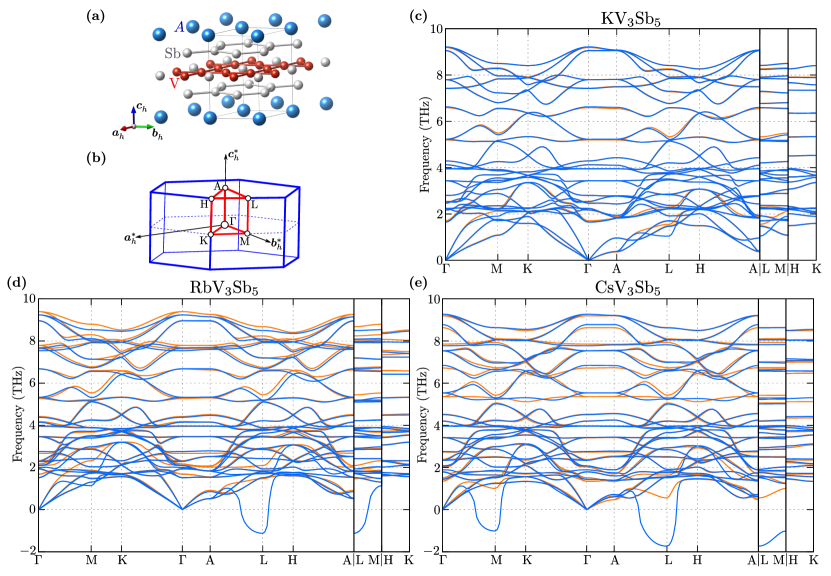
In the room temperature, the V3Sb5 compounds crystallize in the the hexagonal symmetry. Crystal structure, shown in Fig. 1(a), contains the ideal kagome net of atoms (decorated by one Sb atom), sandwiched by two honeycomb nets of Sb atoms (details of the crystal structure are given in the SM [99]). Taking the generic common description presented in the SM [99], system possesses only three structural degrees of freedom ( and lattice constants, and -coordinate describing the position of Sb atom in honeycomb layer). The irreducible representations (IR) at the point are: for acoustic modes, and for optical modes. Only , , and modes are Raman active, while and modes are infra-red active.
To examine the relationship between the CDW phase and the lattice dynamics of the studied compounds, we calculated the phonon dispersion relations at two temperatures strictly related with the emergence of the CDW. The dispersion curves obtained for V3Sb5 systems at 150 K (above ) and 50 K (below ) are demonstrated in Fig. 1 as orange and blue lines, respectively. In the case of heavy ions, i.e. in RbV3Sb5 and CsV3Sb5, we observed the imaginary modes for . In the first case, the imaginary mode at the L point and the small frequency softening at the M point are observed, while in the second, two imaginary modes are found at the M and L points. Imaginary frequency modes lead to the structural phase transition, which will be discussed in more detail in the next subsection. We did not observe any imaginary modes in KV3Sb5 compound, however, the frequencies of both modes, at the M and L points, are slightly reduced at 50 K. The imaginary frequencies are present when the phonon dispersion relations are calculated at T = 0 K [85, 40, 68] thus we assume that all three compounds transform to the lower symmetry phase in the same way.
III.2 Structural phase transition to
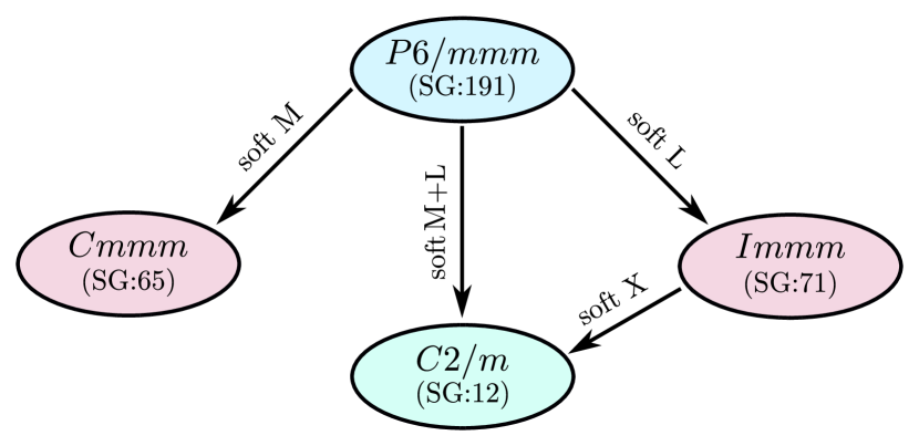
Symmetry analyses of soft modes gives information about the possible stable structures (Fig. 2) for studied systems. First of all, the soft mode at the M point can induce a transition to the symmetry (space group ), while the soft mode at the L point to the symmetry (space group ). It is important to note, that the lowest soft mode typically leads to the most energetically favorable structure. In our case, this corresponds to the soft modes at the L point, which not only change the atom positions, but also generate distortion of the lattice. What is more, dynamical study of the obtained structure with the symmetry leads to another soft mode (at the X point) resulting in a stable structure. This structure can be also found as a result of simultaneous condensation of both soft modes from the M and L points.
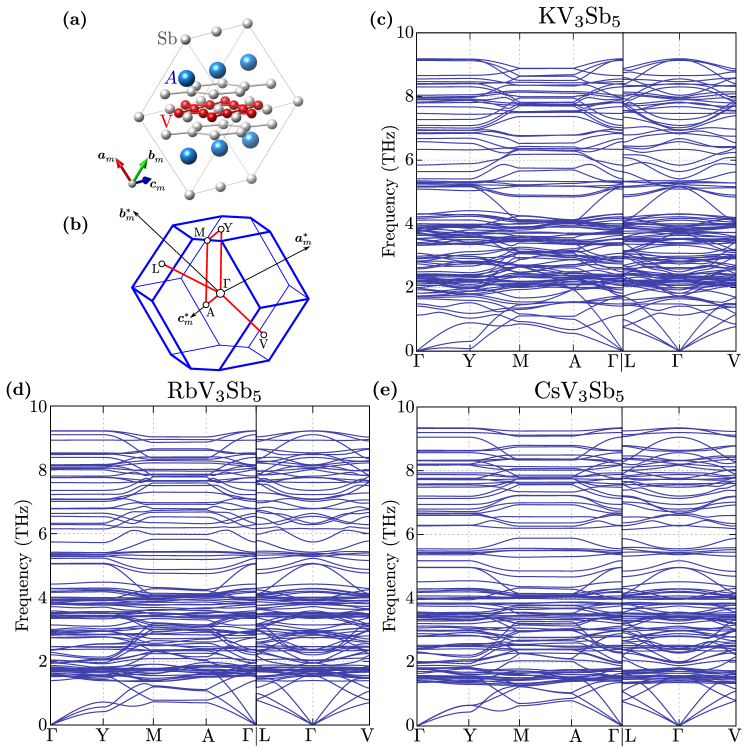
Structure with the symmetry [presented in Fig. 3(a)] does not exhibit any soft modes for any of the V3Sb5 compounds 222Notice, that the distortion introduced by-hand in form of Star of David or inverse Star of David can give positive phonon spectra, see Ref. [38] and [40].. Phonon dispersions [Figs. 3(c)-(e)] are characterized by many nearly flat-bands, as a consequence of the Brillouin zone folding (in relation to the basic symmetry). The IRs at the point are: for acoustic modes, and for optical modes. , and modes are Raman active, while and modes are infra-red active.
Now, we will discuss the atomic displacements during the transition from the to phase because the analysis of the atoms rearrangement may shed new light on the CDW phase of V3Sb5. Both phases have a layered framework and the corresponding layers can be easily compared [cf. Fig. 1(a) and Fig. 3(a)]. We will discuss this question on the example of CsV3Sb3. First, the atoms change position in the direction perpendicular to the layers (along initial direction). The V atoms, on the contrary, are moved only in the plane of the layer. Finally, Sb atoms have rather complex behavior— some of them remain at original positions, while the rest of them is shifted (mostly in direction). The biggest displacements are observed in the case of V atoms (even up to Å) and some Sb atoms (smaller than Å).
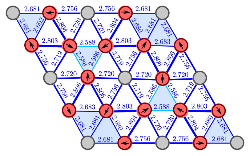
As far as the features of CDW phase are concerned, the most important one is the layer containing V atoms forming kagome net in the structure (or distorted kagome-like net in ). In Fig. 4 we present the differences between atomic positions in the ideal and distorted layer. There, the colored circles correspond to atomic sites in the ideal kagome net layer (the distance between atoms is Å), while solid line circles denote positions of atoms in the distorted lattice of phase. The Sb atoms in the distorted kagome-like layer actually conserve their positions. In contrast to that, the V atoms change their positions significantly. We can define three centers of atomic “attraction” (marked by shaded blue triangles in Fig. 4). Two of them, form isoscales triangles of V atoms, with the distance between atoms equal to Å. Third center is realized in the form of the hexagon of V atoms and centered on Sb atom. In this case, the distance between atoms is equal to Å. As for the rest, the distances between atoms are unchanged or bigger than in the initial structure (detailed values are shown in Fig. 4). Summarizing the above, the low-temperature structure bears the similarity to the inverse SD (tri-hexagonal) structure.
III.3 The phonon density of states and Raman scattering
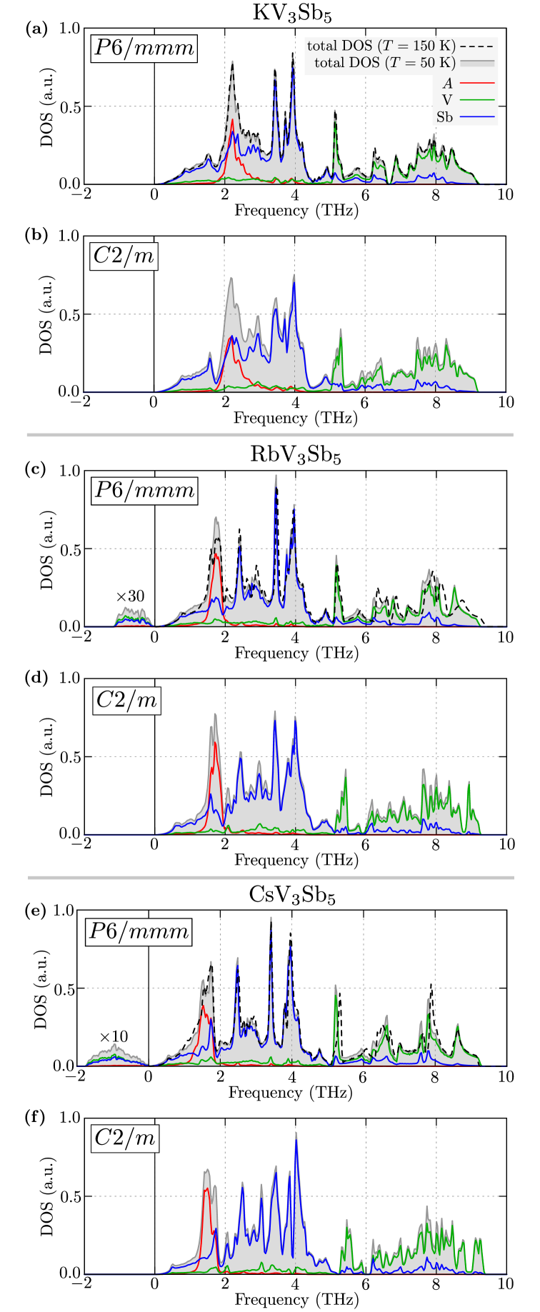
Now, we shortly discuss the phonon density of states (DOS) shown in Fig. 5. For each of the discussed structures (independently of the symmetry), the highest frequency modes (above THz) correspond mostly to vibrations of V atoms (solid green line). Near-flat-bands, located mostly in the middle range of frequencies (from THz to THz) are mainly associated with Sb atoms (solid blue lines). Finally, vibrations of alkali metals are located around THz, and form a clear peak in the DOS (solid red line). In the case of the soft mode DOS, spectral weights clearly show contributions from Sb and V atoms [see Figs. 5(c) and 5(e)]. Additionally, for the structures, we observed a lifting of degeneracy of the band in relation to the symmetry, in the form of multi-peak structure. In practice, this DOS modification is observed in the whole range of frequencies (especially for the contributions that originate from V and Sb atoms).
The frequencies of the Raman modes with their irreducible representations calculated for CsV3Sb5 with the and symmetries are presented in Tab. S3 in SM [99]. The Raman active modes in the structure are present only within the honeycomb Sb sublattices – the mode represents the out-of-plane vibrations, while and are the in-plane modes. The mode is found at THz, in good agreement with the experiments [28, 82, 83]. The frequency of the mode ( THz) is overestimated relative to experimental values, THz [28] and THz [84], while the lowest mode has lower frequency THz than the measured value THz [28]. Our calculations cannot explain the peak at THz observed close to [28], which may be connected with the CDW fluctuations induced by the laser pumping. After phase transition to the structure, the Raman active modes are also associated with other atoms (i.e., Cs and V). In the low-symmetry phase, besides the mode at THz, two additional modes around THz and THZ were observed in the pump-probe experiments [82, 83]. They can be identified as the symmetric modes found here at THz and THz (see Table S3 in SM [99]). The lower mode appears just below , while the higher mode is observed below K. It may indicate the existence of the intermediate phase between with a different symmetry – one of the allowed by the soft modes symmetry [86].
III.4 Surface charge density wave
The CDW phase in V3Sb5 was visualized employing the STM experiment many times [32, 56, 54, 55, 56, 35, 32, 59, 53, 57, 75]. In the case of KV3Sb5, a topography of the Sb layer shows the realization of the surface modulation [53, 57]. Similar results were obtained for the Sb-terminated surface of RbV3Sb5 [75]. However, in this case the additional stripe-like surface structure can be observed in the STM image. Finally, the CDW and stripe superstructures were reported also in the case of the CsV3Sb5 surface [32, 56, 35, 54, 55, 59].
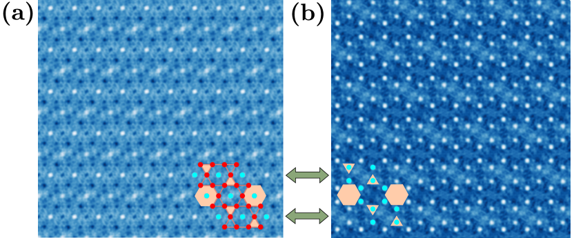
There may be a few reasons for the formation of observed CDW structures. Firstly, the atomic displacements during transition from to symmetry can generate the CDW phase as it is shown earlier in Sec. III.2. Secondly, the surface reconstruction can play an important role in the emergence of the CDW pattern in the STM experiments. To explore this issue, we performed the DFT calculations to simulate STM images for a low-temperature monoclinic phase of CsV3Sb5 (Fig. 6). In the figure, among the complex charge modulations we can identify a clear unidirectional stripes (pointed out by arrows) running along one of the lattice directions (horizontal lines). For clarity, we mark also positions of V and Sb atoms by red and cyan dots, respectively, and positions of the adjacent V atoms in kagome-like plane by orange triangles and hexagons (cf. Fig. 4).
In the case of V kagome-like plane termination [shown in Fig. 6(a)], we observe a stripe-like structure corresponding to the pattern realized by the adjacent V atoms (mostly marked hexagonal shapes). This finding agrees with the previous observation that the CDW phase in this plane is realized by the bonding of vanadium orbitals [73]. Certain refinement can be given also by the shifts of the Sb atoms out of this plane since the realization of the vacuum state from one-site of this plane leads to the small displacement of the Sb atoms in the out-of-plane (vacuum) direction. And then the positions of V atoms are modified, reconstructing a nearly-ideal kagome lattice.
In the case of the Sb-terminated surface [see Fig. 6(b)], we also observe the stripe-like structure. Emergence of the CDW on this surface indirectly corresponds to the inverted SD structure. Here, the surface charge distribution is governed mainly by the orbitals of Sb atoms. However, as we show earlier, the distorted kagome-like plane disturbs the positions of the Sb atoms of neighboring layers, so consequently, the influence of 3D (bulk) CDW is also noticeable in this surface. Similar effect was observed by studying the surface states of Bi2Se3 where the surface charges were modified by the vacancies or atom substitution in the interior of bulk material [105, 106, 107], due to realization of long-range orbital hybridization [108]. Concluding, the observed stripe-like superstructure is related to a subtle effects of the surface reconstruction and the atomic orbitals hybridization rather than an exact 3D CDW emerging in the V3Sb5.
III.5 Electronic properties
The theoretical study of the optical conductivity in CsV3Sb5 [109, 69] shows that the phase transition to the CDW phase is manifested as the transfer of spectral weight towards the higher energies, indicating a partial gap opening and moreover, the reduction in the density of states at the Fermi level. Indeed, the spectral weight suppression around the Fermi level was also observed experimentally, in particular in KV3Sb5 [53], RbV3Sb5 [58] or CsV3Sb5 [32]. In this context, van Hove singularities (VHS) were also studied in many papers [68, 65]. For example, in the case of CsV3Sb5 multiple VHS, emerging from / and / kagome bands [64], coexist near the Fermi level. Additionally, the doping and pressure can tune the VHS closer to the Fermi level, which can also result in different Fermi surface instabilities [71]. Also, the band reconstruction due to system folding and a surface induced orbital-selective shift of the electron energy band were observed in ARPES experiments, e.g. in KV3Sb5 [23] or in CsV3Sb5 [66, 70].
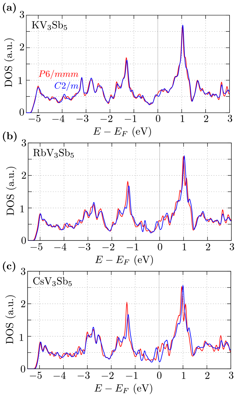
Now, we shortly discuss the electronic properties of the V3Sb5 in the context of its band structure (Fig. S1 in the SM [99]) and DOS (Fig. 7). In the case of the symmetry (top panels in Fig. S1 in the SM [99]), electronic band structures obtained for the primitive cell are in good agreement with the previous studies. In each case, the band structure is formed mostly by V orbitals [73, 71, 24, 76]. Realization of the ideal kagome lattice by V atoms leads to the occurrence of a nearly-flat band around eV, and the corresponding peak in electronic DOS (Fig. 7). At the K and M points, the Dirac points and saddle points are observed around the Fermi level, respectively. This result is consistent with the previous ab initio studies of these compounds [15, 43, 50, 71, 72, 73, 65, 64].
Emergence of the 3D CDW within the supercell of system leads to the above mentioned folding of the Brillouin zone and thus induces the band structure reconstruction (middle panels on Fig. S1 in the SM [99]). In the band structure, new hole-like structures can be identified (marked by pink dotted lines). Indeed, this type of band structure reconstruction is observed in the ARPES experiments [66, 23]. Furthermore, emergence of the similar structures can be observed for the supercell (bottom panels in Fig. S1 in the SM [99]). In this case, additional effects of the band degeneracy lifting in high symmetry points can be observed. As we can see, in the case of both and supercells, their band structure looks similar. Remarkably, such an effect was reported previously [110, 86] in the case of other supercells (e.g. with SD or inverted SD pattern introduced by-hand to the system).
Lowering the symmetry and lifting the band degeneracy (also at the saddle point) around the Fermi level generates a V-shape gap in the DOS spectrum exactly at the Fermi level (see Fig. 7). Similar effect was reported previously – it influences the CDW phase. Here, we clearly show that this is a consequence of the structural phase transition. However, emergence of the additional CDW order should also lead to gap opening. Therefore, this particular aspect of this study is still under debate.
IV Summary and conclusion
In this paper we have discussed the origin of the charge density wave in the V3Sb5 compounds from the microscopic point of view using the ab initio study of their dynamical properties. First, we showed that the structural phase transition at can be realized due to symmetry breaking from the to . Next, we demonstrated that the atomic displacement during this transition leads to emergence of the inverse Star of David pattern. This mechanism can be the source of the 3D charge density wave observed in these compounds. Additionally, the stripe superstructure observed experimentally on the surface of V3Sb5 family can be a consequence of the surface reconstruction.
In our study, we used a thermal multi-displacement technique to find high-order phonon contributions. Notably, lowering symmetry and stabilization of the system with the symmetry is a consequence of the soft modes in the fundamental crystal structure with symmetry. The first-order structural transition can occur directly due to the synergy between soft modes from the M and L points. We have found that, in practice, all of the atoms are shifted from their original high symmetry positions, which suggests that the emergence of more complex charge density wave phase is more likely than it was previously assumed. Stemming from this, analyses of the atoms displacement confirm the appearance of the inverse Star of David pattern, within the distorted kagome-like layer.
Possible manifestation of the phase in V3Sb5 provides an opportunity to observe experimentally the emergence of charge density wave phase by Raman active modes in the phonon spectrum. Indeed, it was recently observed for . Experimental observations of the folding of the Brillouin zone and the reconstruction of electronic band structure were also reproduced. In addition, lifting of the electronic band degeneracy leads to modification of the DOS at the Fermi level, in agreement with experimental results.
Acknowledgements.
Some figures in this work was rendered using Vesta [111]. This work was supported by National Science Centre (NCN, Poland) under Projects No. 2017/24/C/ST3/00276 (A.P.), 2018/31/N/ST3/01746 (A.K.), 2016/23/B/ST3/00839 (A.M.O.), and 2017/25/B/ST3/02586 (P.P.). In addition, A.P. appreciates funding in the frame of scholarships of the Minister of Science and Higher Education of Poland for outstanding young scientists (2019 edition, No. 818/STYP/14/2019).References
- Ye et al. [2018] L. Ye, M. Kang, J. Liu, F. von Cube, C. R. Wicker, T. Suzuki, C. Jozwiak, A. Bostwick, E. Rotenberg, D. C. Bell, L. Fu, R. Comin, and J. G. Checkelsky, Massive Dirac fermions in a ferromagnetic kagome metal, Nature 555, 638 (2018).
- Lin et al. [2018] Z. Lin, J.-H. Choi, Q. Zhang, W. Qin, S. Yi, P. Wang, L. Li, Y. Wang, H. Zhang, Z. Sun, L. Wei, S. Zhang, T. Guo, Q. Lu, J.-H. Cho, C. Zeng, and Z. Zhang, Flatbands and emergent ferromagnetic ordering in Fe3Sn2 kagome lattices, Phys. Rev. Lett. 121, 096401 (2018).
- Sales et al. [2019] B. C. Sales, J. Yan, W. R. Meier, A. D. Christianson, S. Okamoto, and M. A. McGuire, Electronic, magnetic, and thermodynamic properties of the kagome layer compound FeSn, Phys. Rev. Materials 3, 114203 (2019).
- Meier et al. [2020] W. R. Meier, M.-H. Du, S. Okamoto, N. Mohanta, A. F. May, M. A. McGuire, C. A. Bridges, G. D. Samolyuk, and B. C. Sales, Flat bands in the CoSn-type compounds, Phys. Rev. B 102, 075148 (2020).
- Kang et al. [2020] M. Kang, S. Fang, L. Ye, H. C. Po, J. Denlinger, C. Jozwiak, A. Bostwick, E. Rotenberg, E. Kaxiras, J. G. Checkelsky, and R. Comin, Topological flat bands in frustrated kagome lattice CoSn, Nat. Commun. 11, 4004 (2020).
- Chen et al. [2014] H. Chen, Q. Niu, and A. H. MacDonald, Anomalous Hall effect arising from noncollinear antiferromagnetism, Phys. Rev. Lett. 112, 017205 (2014).
- Ko et al. [2009] W.-H. Ko, P. A. Lee, and X.-G. Wen, Doped kagome system as exotic superconductor, Phys. Rev. B 79, 214502 (2009).
- Guo and Franz [2009] H.-M. Guo and M. Franz, Topological insulator on the kagome lattice, Phys. Rev. B 80, 113102 (2009).
- Gardner et al. [2010] J. S. Gardner, M. J. P. Gingras, and J. E. Greedan, Magnetic pyrochlore oxides, Rev. Mod. Phys. 82, 53 (2010).
- Nussinov and van den Brink [2015] Z. Nussinov and J. van den Brink, Compass models: Theory and physical motivations, Rev. Mod. Phys. 87, 1 (2015).
- Ohgushi et al. [2000] K. Ohgushi, S. Murakami, and N. Nagaosa, Spin anisotropy and quantum Hall effect in the kagomé lattice: Chiral spin state based on a ferromagnet, Phys. Rev. B 62, R6065 (2000).
- Han et al. [2012] T.-H. Han, J. S. Helton, S. Chu, D. G. Nocera, J. A. Rodriguez-Rivera, C. Broholm, and Y. S. Lee, Fractionalized excitations in the spin-liquid state of a kagome-lattice antiferromagnet, Nature 492, 406 (2012).
- Zhou et al. [2017] Y. Zhou, K. Kanoda, and T.-K. Ng, Quantum spin liquid states, Rev. Mod. Phys. 89, 025003 (2017).
- Chen et al. [2019] H. Chen, W. Wu, S. A. Yang, X. Li, and L. Zhang, Chiral phonons in kagome lattices, Phys. Rev. B 100, 094303 (2019).
- Ortiz et al. [2019] B. R. Ortiz, L. C. Gomes, J. R. Morey, M. Winiarski, M. Bordelon, J. S. Mangum, I. W. H. Oswald, J. A. Rodriguez-Rivera, J. R. Neilson, S. D. Wilson, E. Ertekin, T. M. McQueen, and E. S. Toberer, New kagome prototype materials: discovery of KV3Sb5, RbV3Sb5, and CsV3Sb5, Phys. Rev. Materials 3, 094407 (2019).
- Yang et al. [2020] S.-Y. Yang, Y. Wang, B. R. Ortiz, D. Liu, J. Gayles, E. Derunova, R. Gonzalez-Hernandez, L. Šmejkal, Y. Chen, S. S. P. Parkin, S. D. Wilson, E. S. Toberer, T. McQueen, and M. N. Ali, Giant, unconventional anomalous Hall effect in the metallic frustrated magnet candidate, KV3Sb5, Sci. Adv. 6, eabb6003 (2020).
- Yu et al. [2021a] F. H. Yu, T. Wu, Z. Y. Wang, B. Lei, W. Z. Zhuo, J. J. Ying, and X. H. Chen, Concurrence of anomalous Hall effect and charge density wave in a superconducting topological kagome metal, Phys. Rev. B 104, L041103 (2021a).
- Zheng et al. [2021] G. Zheng, Z. Chen, C. Tan, M. Wang, X. Zhu, S. Albarakati, M. Algarni, J. Partridge, L. Farrar, J. Zhou, W. Ning, M. Tian, M. S. Fuhrer, and L. Wang, Gate-controllable giant anomalous hall effect from flat bands in kagome metal CsV3Sb5 nanoflakes (2021), arXiv:2109.12588 .
- Kenney et al. [2021] E. M. Kenney, B. R. Ortiz, C. Wang, S. D. Wilson, and M. J. Graf, Absence of local moments in the kagome metal KV3Sb5 as determined by muon spin spectroscopy, J. Phys.: Condens. Matter 33, 235801 (2021).
- Ortiz et al. [2021a] B. R. Ortiz, P. M. Sarte, E. M. Kenney, M. J. Graf, S. M. L. Teicher, R. Seshadri, and S. D. Wilson, Superconductivity in the kagome metal KV3Sb5, Phys. Rev. Materials 5, 034801 (2021a).
- Ortiz et al. [2020] B. R. Ortiz, S. M. L. Teicher, Y. Hu, J. L. Zuo, P. M. Sarte, E. C. Schueller, A. M. M. Abeykoon, M. J. Krogstad, S. Rosenkranz, R. Osborn, R. Seshadri, L. Balents, J. He, and S. D. Wilson, CsV3Sb5: A topological kagome metal with a superconducting ground state, Phys. Rev. Lett. 125, 247002 (2020).
- Setty et al. [2021] C. Setty, H. Hu, L. Chen, and Q. Si, Electron correlations and -breaking density wave order in a kagome metal (2021), arXiv:2105.15204 .
- Luo et al. [2021a] H. Luo, Q. Gao, H. Liu, Y. Gu, D. Wu, C. Yi, J. Jia, S. Wu, X. Luo, Y. Xu, L. Zhao, Q. Wang, H. Mao, G. Liu, Z. Zhu, Y. Shi, K. Jiang, J. Hu, Z. Xu, and X. J. Zhou, Electronic nature of charge density wave and electron-phonon coupling in kagome superconductor KV3Sb5 (2021a), arXiv:2107.02688 .
- Zhao et al. [2021a] J. Zhao, W. Wu, Y. Wang, and S. A. Yang, Electronic correlations in the normal state of the kagome superconductor KV3Sb5, Phys. Rev. B 103, L241117 (2021a).
- Hu et al. [2021a] Y. Hu, S. M. L. Teicher, B. R. Ortiz, Y. Luo, S. Peng, L. Huai, J. Z. Ma, N. C. Plumb, S. D. Wilson, J. F. He, and M. Shi, Charge-order-assisted topological surface states and flat bands in the kagome superconductor CsV3Sb5 (2021a), arXiv:2104.12725 .
- Fu et al. [2021] Y. Fu, N. Zhao, Z. Chen, Q. Yin, Z. Tu, C. Gong, C. Xi, X. Zhu, Y. Sun, K. Liu, and H. Lei, Quantum transport evidence of topological band structures of kagome superconductor CsV3Sb5 (2021), arXiv:2104.08193 .
- Wang et al. [2020] Y. Wang, S. Yang, P. K. Sivakumar, B. R. Ortiz, S. M. L. Teicher, H. Wu, A. K. Srivastava, C. Garg, D. Liu, S. S. P. Parkin, E. S. Toberer, T. McQueen, S. D. Wilson, and M. N. Ali, Proximity-induced spin-triplet superconductivity and edge supercurrent in the topological kagome metal, K1-xV3Sb5 (2020), arXiv:2012.05898 .
- Li et al. [2021a] H. Li, T. T. Zhang, T. Yilmaz, Y. Y. Pai, C. E. Marvinney, A. Said, Q. W. Yin, C. S. Gong, Z. J. Tu, E. Vescovo, C. S. Nelson, R. G. Moore, S. Murakami, H. C. Lei, H. N. Lee, B. J. Lawrie, and H. Miao, Observation of unconventional charge density wave without acoustic phonon anomaly in kagome superconductors V3Sb5 (=Rb, Cs), Phys. Rev. X 11, 031050 (2021a).
- Zhu et al. [2021] C. C. Zhu, X. F. Yang, W. Xia, Q. W. Yin, L. S. Wang, C. C. Zhao, D. Z. Dai, C. P. Tu, B. Q. Song, Z. C. Tao, Z. J. Tu, C. S. Gong, H. C. Lei, Y. F. Guo, and S. Y. Li, Double-dome superconductivity under pressure in the -based kagome metals V3Sb5 ( = Rb and K) (2021), arXiv:2104.14487 .
- Yin et al. [2021] Q. Yin, Z. Tu, C. Gong, Y. Fu, S. Yan, and H. Lei, Superconductivity and normal-state properties of kagome metal RbV3Sb5 single crystals, Chinese Phys. Lett. 38, 037403 (2021).
- Zhao et al. [2021b] C. C. Zhao, L. S. Wang, W. Xia, Q. W. Yin, J. M. Ni, Y. Y. Huang, C. P. Tu, Z. C. Tao, Z. J. Tu, C. S. Gong, H. C. Lei, Y. F. Guo, X. F. Yang, and S. Y. Li, Nodal superconductivity and superconducting domes in the topological kagome metal CsV3Sb5 (2021b), arXiv:2102.08356 .
- Liang et al. [2021] Z. Liang, X. Hou, F. Zhang, W. Ma, P. Wu, Z. Zhang, F. Yu, J.-J. Ying, K. Jiang, L. Shan, Z. Wang, and X.-H. Chen, Three-dimensional charge density wave and surface-dependent vortex-core states in a kagome superconductor CsV3Sb5, Phys. Rev. X 11, 031026 (2021).
- Mu et al. [2021] C. Mu, Q. Yin, Z. Tu, C. Gong, H. Lei, Z. Li, and J. Luo, -wave superconductivity in kagome metal CsV3Sb5 revealed by 121/123Sb and 51V NMR measurements, Chin. Phys. Lett. 38, 077402 (2021).
- Song et al. [2021a] D. W. Song, L. X. Zheng, F. H. Yu, J. Li, L. P. Nie, M. Shan, D. Zhao, S. J. Li, B. L. Kang, Z. M. Wu, Y. B. Zhou, K. L. Sun, K. Liu, X. G. Luo, Z. Y. Wang, J. J. Ying, X. G. Wan, T. Wu, and X. H. Chen, Orbital ordering and fluctuations in a kagome superconductor CsV3Sb5 (2021a), arXiv:2104.09173 .
- Wang et al. [2021a] Z. Wang, Y.-X. Jiang, J.-X. Yin, Y. Li, G.-Y. Wang, H.-L. Huang, S. Shao, J. Liu, P. Zhu, N. Shumiya, M. S. Hossain, H. Liu, Y. Shi, J. Duan, X. Li, G. Chang, P. Dai, Z. Ye, G. Xu, Y. Wang, H. Zheng, J. Jia, M. Z. Hasan, and Y. Yao, Electronic nature of chiral charge order in the kagome superconductor CsV3Sb5, Phys. Rev. B 104, 075148 (2021a).
- Yu et al. [2021b] L. Yu, C. Wang, Y. Zhang, M. Sander, S. Ni, Z. Lu, S. Ma, Z. Wang, Z. Zhao, H. Chen, K. Jiang, Y. Zhang, H. Yang, F. Zhou, X. Dong, S. L. Johnson, M. J. Graf, J. Hu, H.-J. Gao, and Z. Zhao, Evidence of a hidden flux phase in the topological kagome metal CsV3Sb5 (2021b), arXiv:2107.10714 .
- Gupta et al. [2021] R. Gupta, D. Das, C. H. M. III, Z. Guguchia, T. Shiroka, C. Baines, M. Bartkowiak, H. Luetkens, R. Khasanov, Q. Yin, Z. Tu, C. Gong, and H. Lei, Microscopic evidence for anisotropic multigap superconductivity in the CsV3Sb5 kagome superconductor (2021), arXiv:2108.01574 .
- Wang et al. [2021b] Q. Wang, P. Kong, W. Shi, C. Pei, C. Wen, L. Gao, Y. Zhao, Q. Yin, Y. Wu, G. Li, H. Lei, J. Li, Y. Chen, S. Yan, and Y. Qi, Charge density wave orders and enhanced superconductivity under pressure in the kagome metal CsV3Sb5, Adv. Mater. , 2102813 (2021b).
- Ni et al. [2021] S. Ni, S. Ma, Y. Zhang, J. Yuan, H. Yang, Z. Lu, N. Wang, J. Sun, Z. Zhao, D. Li, S. Liu, H. Zhang, H. Chen, K. Jin, J. Cheng, L. Yu, F. Zhou, X. Dong, J. Hu, H.-J. Gao, and Z. Zhao, Anisotropic superconducting properties of kagome metal CsV3Sb5, Chinese Phys. Lett. 38, 057403 (2021).
- Tan et al. [2021] H. Tan, Y. Liu, Z. Wang, and B. Yan, Charge density waves and electronic properties of superconducting kagome metals, Phys. Rev. Lett. 127, 046401 (2021).
- Wu et al. [2021] X. Wu, T. Schwemmer, T. Müller, A. Consiglio, G. Sangiovanni, D. D. Sante, Y. Iqbal, W. Hanke, A. P. Schnyder, M. M. Denner, M. H. Fischer, T. Neupert, and R. Thomale, Nature of unconventional pairing in the kagome superconductors V3Sb5 (2021), arXiv:2104.05671 .
- Song et al. [2021b] B. Q. Song, X. M. Kong, W. Xia, Q. W. Yin, C. P. Tu, C. C. Zhao, D. Z. Dai, K. Meng, Z. C. Tao, Z. J. Tu, C. S. Gong, H. C. Lei, Y. F. Guo, X. F. Yang, and S. Y. Li, Competing superconductivity and charge-density wave in kagome metal CsV3Sb5: evidence from their evolutions with sample thickness (2021b), arXiv:2105.09248 .
- Song et al. [2021c] Y. Song, T. Ying, X. Chen, X. Han, Y. Huang, X. Wu, A. P. Schnyder, J.-G. Guo, and X. Chen, Enhancement of superconductivity in hole-doped CsV3Sb5 thin films (2021c), arXiv:2105.09898 .
- Wang et al. [2021c] T. Wang, A. Yu, H. Zhang, Y. Liu, W. Li, W. Peng, Z. Di, D. Jiang, and G. Mu, Enhancement of the superconductivity and quantum metallic state in the thin film of superconducting kagome metal KV3Sb5 (2021c), arXiv:2105.07732 .
- Du et al. [2021a] F. Du, S. Luo, B. R. Ortiz, Y. Chen, W. Duan, D. Zhang, X. Lu, S. D. Wilson, Y. Song, and H. Yuan, Pressure-induced double superconducting domes and charge instability in the kagome metal KV3Sb5, Phys. Rev. B 103, L220504 (2021a).
- Wang et al. [2021d] N. N. Wang, K. Y. Chen, Q. W. Yin, Y. N. N. Ma, B. Y. Pan, X. Yang, X. Y. Ji, S. L. Wu, P. F. Shan, S. X. Xu, Z. J. Tu, C. S. Gong, G. T. Liu, G. Li, Y. Uwatoko, X. L. Dong, H. C. Lei, J. P. Sun, and J. G. Cheng, Competition between charge-density-wave and superconductivity in the kagome metal RbV3Sb5 (2021d), arXiv:2107.00269 .
- Du et al. [2021b] F. Du, S. Luo, R. Li, B. R. Ortiz, Y. Chen, S. D. Wilson, Y. Song, and H. Yuan, Evolution of superconductivity and charge order in pressurized RbV3Sb5 (2021b), arXiv:2108.09434 .
- Yu et al. [2021c] F. H. Yu, D. H. Ma, W. Z. Zhuo, S. Q. Liu, X. K. Wen, B. Lei, J. J. Ying, and X. H. Chen, Unusual competition of superconductivity and charge-density-wave state in a compressed topological kagome metal, Nat. Commun. 12, 3645 (2021c).
- Chen et al. [2021a] K. Y. Chen, N. N. Wang, Q. W. Yin, Y. H. Gu, K. Jiang, Z. J. Tu, C. S. Gong, Y. Uwatoko, J. P. Sun, H. C. Lei, J. P. Hu, and J.-G. Cheng, Double superconducting dome and triple enhancement of T in the kagome superconductor CsV3Sb5 under high pressure, Phys. Rev. Lett. 126, 247001 (2021a).
- Chen et al. [2021b] X. Chen, X. Zhan, X. Wang, J. Deng, X.-B. Liu, X. Chen, J.-G. Guo, and X. Chen, Highly robust reentrant superconductivity in CsV3Sb5 under pressure, Chinese Phys. Lett. 38, 057402 (2021b).
- Qian et al. [2021] T. Qian, M. H. Christensen, C. Hu, A. Saha, B. M. Andersen, R. M. Fernandes, T. Birol, and N. Ni, Revealing the competition between charge-density wave and superconductivity in CsV3Sb5 through uniaxial strain (2021), arXiv:2107.04545 .
- Zhang et al. [2021a] Z. Zhang, Z. Chen, Y. Zhou, Y. Yuan, S. Wang, J. Wang, H. Yang, C. An, L. Zhang, X. Zhu, Y. Zhou, X. Chen, J. Zhou, and Z. Yang, Pressure-induced reemergence of superconductivity in the topological kagome metal CsV3Sb5, Phys. Rev. B 103, 224513 (2021a).
- Jiang et al. [2021] Y.-X. Jiang, J.-X. Yin, M. M. Denner, N. Shumiya, B. R. Ortiz, G. Xu, Z. Guguchia, J. He, M. S. Hossain, X. Liu, J. Ruff, L. Kautzsch, S. S. Zhang, G. Chang, I. Belopolski, Q. Zhang, T. A. Cochran, D. Multer, M. Litskevich, Z.-J. Cheng, X. P. Yang, Z. Wang, R. Thomale, T. Neupert, S. D. Wilson, and M. Z. Hasan, Unconventional chiral charge order in kagome superconductor KV3Sb5, Nat. Mater. 20, 1353 (2021).
- Li et al. [2021b] H. Li, S. Wan, H. Li, Q. Li, Q. Gu, H. Yang, Y. Li, Z. Wang, Y. Yao, and H.-H. Wen, No indication of chiral flux current in the topological kagome metal CsV3Sb5 (2021b), arXiv:2107.11326 .
- Zhao et al. [2021c] H. Zhao, H. Li, B. R. Ortiz, S. M. L. Teicher, T. Park, M. Ye, Z. Wang, L. Balents, S. D. Wilson, and I. Zeljkovic, Cascade of correlated electron states in a kagome superconductor CsV3Sb5 (2021c), arXiv:2103.03118 .
- Chen et al. [2021c] H. Chen, H. Yang, B. Hu, Z. Zhao, J. Yuan, Y. Xing, G. Qian, Z. Huang, G. Li, Y. Ye, S. Ma, S. Ni, H. Zhang, Q. Yin, C. Gong, Z. Tu, H. Lei, H. Tan, S. Zhou, C. Shen, X. Dong, B. Yan, Z. Wang, and H.-J. Gao, Roton pair density wave in a strong-coupling kagome superconductor, Nature 10.1038/s41586-021-03983-5 (2021c).
- Li et al. [2021c] H. Li, H. Zhao, B. R. Ortiz, T. Park, M. Ye, L. Balents, Z. Wang, S. D. Wilson, and I. Zeljkovic, Rotation symmetry breaking in the normal state of a kagome superconductor KV3Sb5 (2021c), arXiv:2104.08209 .
- Yu et al. [2021d] J. Yu, K. Xiao, Y. Yuan, Q. Yin, Z. Hu, C. Gong, Y. Guo, Z. Tu, H. Lei, Q.-K. Xue, and W. Li, Evolution of electronic structure in pristine and hole-doped kagome metal RbV3Sb5 (2021d), arXiv:2109.11286 .
- Xu et al. [2021] H.-S. Xu, Y.-J. Yan, R. Yin, W. Xia, S. Fang, Z. Chen, Y. Li, W. Yang, Y. Guo, and D.-L. Feng, Multiband superconductivity with sign-preserving order parameter in kagome superconductor CsV3Sb5 (2021), arXiv:2104.08810 .
- Li et al. [2021d] H. Li, Y.-X. Jiang, J. X. Yin, S. Yoon, A. R. Lupini, C. Nelson, A. Said, Y. M. Yang, H. C. Lei, B. Yan, Z. Wang, M. Z. Hasan, H. N. Lee, and H. Miao, Absence of superlattice in bulk kagome superconductor CsV3Sb5 (2021d), arXiv:2109.03418 .
- Nakayama et al. [2021] K. Nakayama, Y. Li, M. Liu, Z. Wang, T. Takahashi, Y. Yao, and T. Sato, Multiple energy scales and anisotropic energy gap in the charge-density-wave phase of kagome superconductor CsV3Sb5 (2021), arXiv:2104.08042 .
- Wang et al. [2021e] Z. Wang, S. Ma, Y. Zhang, H. Yang, Z. Zhao, Y. Ou, Y. Zhu, S. Ni, Z. Lu, H. Chen, K. Jiang, L. Yu, Y. Zhang, X. Dong, J. Hu, H.-J. Gao, and Z. Zhao, Distinctive momentum dependent charge-density-wave gap observed in CsV3Sb5 superconductor with topological kagome lattice (2021e), arXiv:2104.05556 .
- Lou et al. [2021] R. Lou, A. Fedorov, Q. Yin, A. Kuibarov, Z. Tu, C. Gong, E. F. Schwier, B. Büchner, H. Lei, and S. Borisenko, Charge-density-wave-induced peak-dip-hump structure and flat band in the kagome superconductor CsV3Sb5 (2021), arXiv:2106.06497 .
- Kang et al. [2021] M. Kang, S. Fang, J.-K. Kim, B. R. Ortiz, J. Yoo, B.-G. Park, S. D. Wilson, J.-H. Park, and R. Comin, Twofold van hove singularity and origin of charge order in topological kagome superconductor CsV3Sb5 (2021), arXiv:2105.01689 .
- Hu et al. [2021b] Y. Hu, X. Wu, B. R. Ortiz, S. Ju, X. Han, J. Z. Ma, N. C. Plumb, M. Radovic, R. Thomale, S. D. Wilson, A. P. Schnyder, and M. Shi, Rich nature of van Hove singularities in kagome superconductor CsV3Sb5 (2021b), arXiv:2106.05922 .
- Luo et al. [2021b] Y. Luo, S. Peng, S. M. L. Teicher, L. Huai, Y. Hu, B. R. Ortiz, Z. Wei, J. Shen, Z. Ou, B. Wang, Y. Miao, M. Guo, M. Shi, S. D. Wilson, and J. F. He, Distinct band reconstructions in kagome superconductor CsV3Sb5 (2021b), arXiv:2106.01248 .
- Cai et al. [2021] Y. Cai, Y. Wang, Z. Hao, Y. Liu, X.-M. Ma, Z. Shen, Z. Jiang, Y. Yang, W. Liu, Q. Jiang, Z. Liu, M. Ye, D. Shen, Z. Sun, J. Chen, L. Wang, C. Liu, J. Lin, J. Wang, B. Huang, J.-W. Mei, and C. Chen, Emergence of quantum confinement in topological kagome superconductor csv3sb5 family (2021), arXiv:2109.12778 .
- Cho et al. [2021] S. Cho, H. Ma, W. Xia, Y. Yang, Z. Liu, Z. Huang, Z. Jiang, X. Lu, J. Liu, Z. Liu, J. Jia, Y. Guo, J. Liu, and D. Shen, Emergence of new van Hove singularities in the charge density wave state of a topological kagome metal RbV3Sb5 (2021), arXiv:2105.05117 .
- Uykur et al. [2021a] E. Uykur, B. R. Ortiz, S. D. Wilson, M. Dressel, and A. A. Tsirlin, Optical detection of charge-density-wave instability in the non-magnetic kagome metal KV3Sb5 (2021a), arXiv:2103.07912 .
- Ortiz et al. [2021b] B. R. Ortiz, S. M. L. Teicher, L. Kautzsch, P. M. Sarte, J. P. C. Ruff, R. Seshadri, and S. D. Wilson, Fermi surface mapping and the nature of charge density wave order in the kagome superconductor CsV3Sb5 (2021b), arXiv:2104.07230 .
- LaBollita and Botana [2021] H. LaBollita and A. S. Botana, Tuning the van Hove singularities in V3Sb5 ( = K, Rb, Cs) via pressure and doping (2021), arXiv:2108.04876 .
- Zhou et al. [2021] X. Zhou, Y. Li, X. Fan, J. Hao, Y. Dai, Z. Wang, Y. Yao, and H.-H. Wen, Origin of charge density wave in the kagome metal CsV3Sb5 as revealed by optical spectroscopy, Phys. Rev. B 104, L041101 (2021).
- Wang et al. [2021f] C. Wang, S. Liu, H. Jeon, and J.-H. Cho, Origin of charge density wave in layered kagome metal CsV3Sb5 (2021f), arXiv:2109.01921 .
- Christensen et al. [2021] M. H. Christensen, T. Birol, B. M. Andersen, and R. M. Fernandes, Theory of the charge-density wave in V3Sb5 kagome metals (2021), arXiv:2107.04546 .
- Shumiya et al. [2021] N. Shumiya, M. S. Hossain, J.-X. Yin, Y.-X. Jiang, B. R. Ortiz, H. Liu, Y. Shi, Q. Yin, H. Lei, S. S. Zhang, G. Chang, Q. Zhang, T. A. Cochran, D. Multer, M. Litskevich, Z.-J. Cheng, X. P. Yang, Z. Guguchia, S. D. Wilson, and M. Z. Hasan, Intrinsic nature of chiral charge order in the kagome superconductor RbV3Sb5, Phys. Rev. B 104, 035131 (2021).
- Tsirlin et al. [2021] A. A. Tsirlin, P. Fertey, B. R. Ortiz, B. Klis, V. Merkl, M. Dressel, S. D. Wilson, and E. Uykur, Role of sb in the superconducting kagome metal CsV3Sb5 revealed by its anisotropic compression (2021), arXiv:2105.01397 .
- Luo et al. [2021c] J. Luo, Z. Zhao, Y. Z. Zhou, J. Yang, A. F. Fang, H. T. Yang, H. J. Gao, R. Zhou, and G. q. Zheng, Star-of-David pattern charge density wave with additional modulation in the kagome superconductor CsV3Sb5 revealed by 51V-NMR and 121/123Sb-NQR (2021c), arXiv:2108.10263 .
- Denner et al. [2021] M. M. Denner, R. Thomale, and T. Neupert, Analysis of charge order in the kagome metal V3Sb5 (=K,Rb,Cs) (2021), arXiv:2103.14045 .
- Lin and Nandkishore [2021] Y.-P. Lin and R. M. Nandkishore, Complex charge density waves at Van Hove singularity on hexagonal lattices: Haldane-model phase diagram and potential realization in the kagome metals V3Sb5 (=K, Rb, Cs), Phys. Rev. B 104, 045122 (2021).
- III et al. [2021] C. M. III, D. Das, J. X. Yin, H. Liu, R. Gupta, C. N. Wang, Y. X. Jiang, M. Medarde, X. Wu, H. C. Lei, J. J. Chang, P. Dai, Q. Si, H. Miao, R. Thomale, T. Neupert, Y. Shi, R. Khasanov, M. Z. Hasan, H. Luetkens, and Z. Guguchia, Time-reversal symmetry-breaking charge order in a correlated kagome superconductor (2021), arXiv:2106.13443 .
- Park et al. [2021] T. Park, M. Ye, and L. Balents, Electronic instabilities of kagome metals: Saddle points and Landau theory, Phys. Rev. B 104, 035142 (2021).
- Ratcliff et al. [2021] N. Ratcliff, L. Hallett, B. R. Ortiz, S. D. Wilson, and J. W. Harter, Coherent phonon spectroscopy and interlayer modulation of charge density wave order in the kagome metal CsV3Sb5 (2021), arXiv:2104.10138 .
- Wang et al. [2021g] Z. X. Wang, Q. Wu, Q. W. Yin, C. S. Gong, Z. J. Tu, T. Lin, Q. M. Liu, L. Y. Shi, S. J. Zhang, D. Wu, H. C. Lei, T. Dong, and N. L. Wang, Unconventional charge density wave and photoinduced lattice symmetry change in the kagome metal CsV3Sb5 probed by time-resolved spectroscopy, Phys. Rev. B 104, 165110 (2021g).
- Wulferding et al. [2021] D. Wulferding, S. Lee, Y. Choi, Q. Yin, Z. Tu, C. Gong, H. Lei, and K.-Y. Choi, Fermi surface instabilities in electronic Raman scattering of the metallic kagome lattice CsV3Sb5 (2021), arXiv:2108.11690 .
- Zhang et al. [2021b] J.-F. Zhang, K. Liu, and Z.-Y. Lu, First-principles study on the double-dome superconductivities in kagome material CsV3Sb5 under pressure (2021b), arXiv:2106.11477 .
- Subedi [2021] A. Subedi, Hexagonal-to-base-centered-orthorhombic charge density wave order in kagome metals KV3Sb5, RbV3Sb5, and CsV3Sb5 (2021), arXiv:2108.07784 .
- Miao et al. [2021] H. Miao, H. X. Li, H. N. Lee, A. Said, H. C. Lei, J. X. Yin, M. Z. Hasan, Z. Wang, H. Tan, and B. Yan, Geometry of the charge density wave in kagome metal V3Sb5 (2021), arXiv:2106.10150 .
- Blöchl [1994] P. E. Blöchl, Projector augmented-wave method, Phys. Rev. B 50, 17953 (1994).
- Kresse and Hafner [1994] G. Kresse and J. Hafner, Ab initio molecular-dynamics simulation of the liquid-metal–amorphous-semiconductor transition in germanium, Phys. Rev. B 49, 14251 (1994).
- Kresse and Furthmüller [1996] G. Kresse and J. Furthmüller, Efficient iterative schemes for ab initio total-energy calculations using a plane-wave basis set, Phys. Rev. B 54, 11169 (1996).
- Kresse and Joubert [1999] G. Kresse and D. Joubert, From ultrasoft pseudopotentials to the projector augmented-wave method, Phys. Rev. B 59, 1758 (1999).
- Perdew et al. [1996] J. P. Perdew, K. Burke, and M. Ernzerhof, Generalized gradient approximation made simple, Phys. Rev. Lett. 77, 3865 (1996).
- Grimme et al. [2010] S. Grimme, J. Antony, S. Ehrlich, and H. Krieg, A consistent and accurate ab initio parametrization of density functional dispersion correction (DFT-D) for the 94 elements H-Pu, J. Chem. Phys. 132, 154104 (2010).
- Monkhorst and Pack [1976] H. J. Monkhorst and J. D. Pack, Special points for Brillouin-zone integrations, Phys. Rev. B 13, 5188 (1976).
- Stokes and Hatch [2005] H. T. Stokes and D. M. Hatch, FINDSYM: program for identifying the space-group symmetry of a crystal, J. Appl. Crystallogr. 38, 237 (2005).
- Hinuma et al. [2017] Y. Hinuma, G. Pizzi, Y. Kumagai, F. Oba, and I. Tanaka, Band structure diagram paths based on crystallography, Comput. Mater. Sci. 128, 140 (2017).
- Togo and Tanaka [2018] A. Togo and I. Tanaka, Spglib: a software library for crystal symmetry search (2018), arXiv:1808.01590 .
- Tadano et al. [2014] T. Tadano, Y. Gohda, and S. Tsuneyuki, Anharmonic force constants extracted from first-principles molecular dynamics: applications to heat transfer simulations, J. Phys.: Condens. Matter 26, 225402 (2014).
- Note [1] See Supplemental Material at [URL will be inserted by publisher] for details about construction of the supercells and crystallographic data for obtained structures with and symmetries. Supplemental Material contain also additional numerical results and data.
- Hellman et al. [2011] O. Hellman, I. A. Abrikosov, and S. I. Simak, Lattice dynamics of anharmonic solids from first principles, Phys. Rev. B 84, 180301(R) (2011).
- Jochym and Łażewski [2021] P. T. Jochym and J. Łażewski, High Efficiency Configuration Space Sampling – probing the distribution of available states, SciPost Phys. 10, 129 (2021).
- Parlinski et al. [1997] K. Parlinski, Z. Q. Li, and Y. Kawazoe, First-principles determination of the soft mode in cubic ZrO2, Phys. Rev. Lett. 78, 4063 (1997).
- Parlinski [2019] K. Parlinski, Phonon, Cracow (2019).
- Note [2] Notice, that the distortion introduced by-hand in form of Star of David or inverse Star of David can give positive phonon spectra, see Ref. [38] and [40].
- Kim et al. [2011] S. Kim, M. Ye, K. Kuroda, Y. Yamada, E. E. Krasovskii, E. V. Chulkov, K. Miyamoto, M. Nakatake, T. Okuda, Y. Ueda, K. Shimada, H. Namatame, M. Taniguchi, and A. Kimura, Surface scattering via bulk continuum states in the 3D topological insulator Bi2Se3, Phys. Rev. Lett. 107, 056803 (2011).
- Wang et al. [2011] Y.-L. Wang, Y. Xu, Y.-P. Jiang, J.-W. Liu, C.-Z. Chang, M. Chen, Z. Li, C.-L. Song, L.-L. Wang, K. He, X. Chen, W.-H. Duan, Q.-K. Xue, and X.-C. Ma, Structural defects and electronic properties of the Cu-doped topological insulator Bi2Se3, Phys. Rev. B 84, 075335 (2011).
- Jurczyszyn et al. [2020] M. Jurczyszyn, M. Sikora, M. Chrobak, and L. Jurczyszyn, Studies of surface states in Bi2Se3 induced by the BiSe substitution in the crystal subsurface structure, Appl. Surf. Sci. 528, 146978 (2020).
- Ptok et al. [2020] A. Ptok, K. J. Kapcia, and A. Ciechan, Electronic properties of Bi2Se3 dopped by transition metal (Mn, Fe, Co, or Ni) ions, J. Phys.: Condens. Matter 33, 065501 (2020).
- Uykur et al. [2021b] E. Uykur, B. R. Ortiz, O. Iakutkina, M. Wenzel, S. D. Wilson, M. Dressel, and A. A. Tsirlin, Low-energy optical properties of the nonmagnetic kagome metal CsV3Sb5, Phys. Rev. B 104, 045130 (2021b).
- Tang et al. [2021] F. Tang, S. Ono, X. Wan, and H. Watanabe, High-throughput investigations of topological and nodal superconductors (2021), arXiv:2106.11985 .
- Momma and Izumi [2011] K. Momma and F. Izumi, vesta3 for three-dimensional visualization of crystal, volumetric and morphology data, J. Appl. Crystallogr. 44, 1272 (2011).
Supplemental Material
Dynamical Study of the Origin of the Charge Density Wave
in V3Sb5 (K, Rb, Cs) Compounds
Andrzej Ptok,1 Aksel Kobiałka,2 Małgorzata Sternik,1
Paweł T. Jochym,1
Jan Łażewski,1 Andrzej M. Oleś,3,4 and Przemysław Piekarz
1Institute of Nuclear Physics, Polish Academy of Sciences, W. E. Radzikowskiego 152, PL-31342 Kraków, Poland
2Institute of Physics, Maria Curie-Skłodowska University, Plac Marii Skłodowskiej-Curie 1, PL-20031 Lublin, Poland
3Institute of Theoretical Physics, Jagiellonian University, Prof. Stanisława Łojasiewicza 11, PL-30348 Kraków, Poland
4Max Planck Institute for Solid State Research, Heisenbergstrasse 1, D-70569 Stuttgart, Germany
(Dated: )
In this Supplemental Material we present additional results, in particular concerning:
- •
-
•
information about the construction of the conventional cell and supercell used in calculations (Section S1),
-
•
comparison of the electronic band structure for V3Sb5 supercells with different symmetries (Fig. S1),
-
•
the frequencies of the optical modes at the point with the indicated Raman (R) and infrared (Ir) activities for CsV3As5 in and phases (Table S3).
S1 Construction of conventional cell and supercell
Let us start with the introduction of the basis and , denoting the lattice vectors of the primitive unit cells for the tetragonal and monoclinic structure. In the case of the primitive unit cell it is equivalent to the conventional cell. Contrary to this, the conventional cell for can be obtained by the following transformation:
| (S1) |
Values of the lattice vectors in this convention are presented directly in Table S2.
In the phonon calculation we used the supercell with relatively large lattice vectors to minimize the self-interaction between atom and their simulated picture obtained from periodic boundary condition within DFT. In the case of the symmetry, we took the supercell, while for the symmetry a supercell was given by a transformation:
| (S2) |
what gives the lattice vectors with length in range Å.
| symmetry | ||||||
| based atom | K | Rb | Cs | |||
| experimental [15] | theoretical | experimental [15] | theoretical | experimental [15] | theoretical | |
| a (Å) | 5.4818 | 5.4028 | 5.4715 | 5.4154 | 5.4949 | 5.4371 |
| b (Å) | 5.4818 | 5.4028 | 5.4715 | 5.4154 | 5.4949 | 5.4371 |
| c (Å) | 8.9477 | 8.6885 | 9.0733 | 8.8770 | 9.3085 | 9.0520 |
| V (Å3) | 232.86 | 219.64 | 235.24 | 225.45 | 243.41 | 231.74 |
| (1a) | (0,0,0) | |||||
| V (3g) | (1/2,0,1/2) | |||||
| Sb (1b) | (0,0,1/2) | |||||
| Sb (4h) | (1/3,2/3,) | |||||
| 0.7532 | 0.76158 | 0.7498 | 0.75509 | 0.7421 | 0.74919 | |
| symmetry | |||
| based atom | K | Rb | Cs |
| a (Å) | 10.8047 | 10.8299 | 10.8538 |
| b (Å) | 17.3850 | 17.7788 | 18.3590 |
| c (Å) | 10.8096 | 10.8299 | 10.8643 |
| V (Å3) | 1758.72 | 1807.89 | 1875.45 |
| () | 90 | ||
| () | 119.975 | ||
| () | 90 | ||
| (4g) | (0,1/4,0) | ||
| (4h) | (0,0.2493,1/2) | (0,0.2490,1/2) | (0,0.2489,1/2) |
| V (4i) | (0.00112,00.2519) | (0.0006,0,0.2529) | (0.0001,0,0.2535) |
| V (4i) | (0.2485,0,1/2) | (0.2473,0,1/2) | (0.2466,0,1/2) |
| V (4i) | (0.2493,0,0.7481) | (0.2477,0,0.7471) | (0.2466,0,0.7465) |
| V (4i) | (0.2514,0,0.2479) | (0.2531,0,0.2466) | (0.2541,0,0.0082) |
| V (4i) | (0.2523,0,0.0046) | (0.2535,0,0.0071) | (0.2540,0,0.2459) |
| V (4i) | (0.4965,0,0.2479) | (0.4935,0,0.2466) | (0.4920,0,0.2459) |
| Sb (2a) | (0,0,0) | ||
| Sb (2b) | (0,1/2,0) | ||
| Sb (2c) | (0,0,1/2) | ||
| Sb (2d) | (0,1/2,1/2) | ||
| Sb (8j) | (0.1670,0.1305,0.3333) | (0.1672,0.1268,0.3331) | (0.1673,0.1221,0.3329) |
| Sb (8j) | (0.1663,0.3695,0.3333) | (0.1659,0.3732,0.3331) | (0.1656,0.3779,0.3329) |
| Sb (8j) | (0.3334,0.1318,0.1667) | (0.3334,0.1293,0.1667) | (0.3334,0.1251,0.1667) |
| Sb (8j) | (0.3332,0.3700,0.1664) | (0.3330,0.3735,0.1659) | (0.3328,0.3780,0.1655) |

| (THz) | IR | (THz) | IR | (THz) | IR | (THz) | IR |
|---|---|---|---|---|---|---|---|
| 1.505 | (Ir) | 1.332 | (Ir) | 1.401 | (R) | 1.412 | (Ir) |
| 1.763 | (Ir) | 1.421 | (R) | 1.447 | (Ir) | 1.481 | (R) |
| 2.047 | 1.502 | (Ir) | 1.509 | (Ir) | 1.515 | (R) | |
| 2.120 | (Ir) | 1.519 | (R) | 1.547 | (R) | 1.577 | (R) |
| 2.270 | (R) | 1.624 | (Ir) | 1.657 | (R) | 1.740 | (R) |
| 2.808 | (Ir) | 1.759 | (Ir) | 1.790 | (R) | 1.791 | (R) |
| 3.451 | 1.795 | (R) | 1.981 | (Ir) | 1.982 | (Ir) | |
| 3.967 | (R) | 2.040 | (Ir) | 2.046 | (Ir) | 2.118 | (Ir) |
| 4.194 | (R) | 2.368 | (Ir) | 2.376 | (R) | 2.388 | (R) |
| 4.478 | 2.484 | (Ir) | 2.485 | (Ir) | 2.729 | (Ir) | |
| 5.526 | (Ir) | 2.799 | (Ir) | 2.829 | (R) | 2.862 | (Ir) |
| 6.905 | 2.886 | (R) | 2.928 | (Ir) | 2.972 | (Ir) | |
| 7.621 | (Ir) | 2.983 | (Ir) | 3.127 | (R) | 3.160 | (Ir) |
| 7.656 | (Ir) | 3.264 | (Ir) | 3.360 | (R) | 3.448 | (Ir) |
| 8.892 | 3.449 | (R) | 3.454 | (Ir) | 3.462 | (R) | |
| 9.275 | 3.487 | (Ir) | 3.488 | (Ir) | 3.533 | (R) | |
| 3.550 | (R) | 3.733 | (Ir) | 3.744 | (R) | ||
| 3.758 | (Ir) | 3.842 | (R) | 3.856 | (R) | ||
| 3.908 | (R) | 3.933 | (Ir) | 3.940 | (Ir) | ||
| 3.946 | (R) | 3.956 | (R) | 3.974 | (Ir) | ||
| 3.996 | (Ir) | 4.141 | (Ir) | 4.204 | (Ir) | ||
| 4.210 | (R) | 4.218 | (Ir) | 4.515 | (R) | ||
| 4.975 | (Ir) | 4.996 | (Ir) | 5.195 | (Ir) | ||
| 5.205 | (R) | 5.305 | (R) | 5.307 | (R) | ||
| 5.471 | (Ir) | 5.475 | (Ir) | 5.787 | (R) | ||
| 6.251 | (R) | 6.302 | (Ir) | 6.446 | (R) | ||
| 6.512 | (Ir) | 6.554 | (Ir) | 6.808 | (R) | ||
| 6.809 | (R) | 7.001 | (R) | 7.052 | (R) | ||
| 7.233 | (R) | 7.288 | (R) | 7.416 | (Ir) | ||
| 7.597 | (Ir) | 7.632 | (Ir) | 7.646 | (Ir) | ||
| 7.689 | (Ir) | 7.810 | (R) | 8.055 | (R) | ||
| 8.063 | (Ir) | 8.073 | (Ir) | 8.133 | (R) | ||
| 8.236 | (Ir) | 8.248 | (Ir) | 8.309 | (Ir) | ||
| 8.531 | (R) | 8.572 | (R) | 8.899 | (Ir) | ||
| 9.118 | (R) | 9.317 | (Ir) | 9.360 | (Ir) | ||