Substitutional tin acceptor states in black phosphorus
Abstract
Nominally-pure black phosphorus (BP) is commonly found to be a p-type semiconductor, suggesting the ubiquitious presence of impurity species or intrinsic, charged defects. Moreover, scanning tunnelling microscopy (STM) images of black phosphorus reveal the presence of long-ranged double-lobed defect features superimposed onto the surface atomic lattice. We show that both the p-type doping of BP and the defect features observed in STM images can be attributed to substitutional tin impurities. We show that black phosphorus samples produced through two common synthesis pathways contain tin impurities, and we demonstrate that the ground state of substitutional tin impurities is negatively charged for a wide range of Fermi level positions within the BP bandgap. The localised negative charge of the tin impurities induces hydrogenic states in the bandgap and it is the 2p level that sits at the valence band edge that gives rise to the double-lobed features observed in STM images.
London Centre for Nanotechnology, University College London, WC1H 0AH, London, UK \altaffiliationLondon Centre for Nanotechnology, University College London, WC1H 0AH, London, UK \altaffiliationLondon Centre for Nanotechnology, University College London, WC1H 0AH, London, UK
1 Introduction
Black phosphorus (BP) is a two-dimensional (2D) van der Waals layered material and is considered a promising candidate for future (opto)electronic and quantum-electronic devices 1, 2. BP holds a unique position within the family of 2D van der Waals layered materials, being the only mono-elemental 2D material besides graphite 3. Electrical and optical characterisation of nominally pure samples of BP uniformly find the material to be electronically p-type, dating back to the earliest measurements in the 1960s 4, 5, 6, 7, 8. This suggests the ubiquitous presence of charged impurities or structural defects in BP; however, the identity of these impurities/defects, and therefore the source of the p-type doping in BP, remains unexplained. In addition to causing shifts in the Fermi level, atomic point defects can greatly affect the fundamental properties of crystalline materials; for example they can act as nucleation centers for exotic phenomena such as charge density waves or superconducting phases 9, 10. Thus, determining the atomic structure of the intrinsic defects/impurities in BP is of critical importance for both the fundamental understanding of BP, and for nanoelectronic applications.
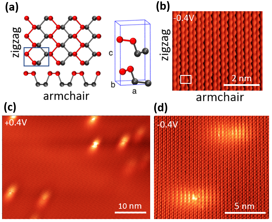
Black phosphorus is comprised of hexagonally bonded sheets of phosphorus atoms, similar to the hexagonally bonded sheets of carbon atoms that form graphene. However, because phosphorus has one extra valence electron than carbon, the phosphorus atoms of BP are hybridised with three bonds to nearest neighbours and an electron lone pair, rather than hybridised with a single electron (per carbon atom) in a orbital as is the case for graphene sheets. This results in the individual phosphorene sheets of BP forming a buckled configuration, as indicated schematically in Fig. 1a. The directions parallel and perpendicular to these rows are conventionally referred to as the zig-zag and armchair directions, respectively. In addition to this strong structural anisotropy, BP also exhibits both in-plane and out-of-plane electronic anisotropy, with the in-plane anisotropy characterised by strong changes in electron effective mass and mobility between the zig-zag and armchair directions 11, 12.
The presence of point defects in nominally intrinsic BP has been confirmed by atomic-resolution scanning tunnelling microscopy (STM) measuremts made by multiple groups 7, 8, 13. The defects appear as long-ranged anisotropic protrusions superimposed on the atomic lattice, and in the literature they have largely been attributed to charged single-phosphorus vacancies 7, 8, 14. However, this assignment is in disagreement with density functional theory (DFT) calculations that demonstrate very small diffusion barriers for monovacancies in BP 15, 16, 17, 18. These low barriers mean that monovacancies can be expected to diffuse much faster than STM scanning times at room temperature, and remain mobile even at 77 K. However, no evidence of diffusion of the defects observed by STM have been reported 7, 8, 14, consistent also with our observations here. DFT calculations also show that monovacancies are unstable with respect to the formation of divacancies. 17 Since divacancies are charge neutral, they are not expected to produce the long-ranged features observed in STM images, nor can they explain the p-type doping observed in BP. Hence vacancy defects do not provide an explanation for the experimentally measured p-type electronic behaviour of BP, or the appearance of the defects observed in STM experiments.
Here, we use a combination of atomic-resolution STM, scanning tunnelling spectroscopy (STS), X-ray photoelectron spectroscopy (XPS), DFT, and tight-binding simulations, to investigate the origin of p-type doping in BP and the long-range defect features observed in STM images of BP. We find that both the p-type doping and the defects seen in STM images can be attributed to substitutional tin impurities in the lattice, which are present due to the use of tin-based catalysts in BP growth, and that produce negatively-charged acceptor states in BP. The characteristic double-lobed appearance of the defects in STM images results mainly from imaging a 2p orbital that exists just inside the bandgap at the valence band edge, with a lesser contribution also from a 1s orbital that lies deep within the bandgap.
2 Methods
2.1 Experimental methods
Scanning Tunnelling microscopy and spectroscopy (STM/STS) measurements were performed using a commercial Scienta Omicron system operating at 77 K with a base pressure below 10-10 mbar. Black phosphorus flakes were purchased from SmartElements and 2DSemiconductors. Samples with large single crystal areas were selected for STM measurement and mounted onto stainless steel sample holder plates using Epotek H21D conductive epoxy. Samples were outgassed in vacuum at 150∘C overnight, before being cleaved in-situ to expose an atomically-clean surface. STM tips were chemically etched from tungsten wire and had their surface oxide removed by electron bombardment in the STM vacuum chamber. STS was performed by measuring the current as a function of the sample voltage with a constant tip-sample separation. X-ray photoemission spectroscopy (XPS) measurements were performed on a Thermo K-alpha system operating at a base pressure of 10-9 mbar. Samples were cleaved ex-situ before rapid transfer into the loadlock and pumping down to 10-6 mbar. Cleaved samples were exposed to ambient conditions for less than one minute.
2.2 Density functional theory calculations
Density functional theory (DFT) was used to calculate the electronic structure of substitutional tin defects in monolayer and multilayer BP. The calculations were performed using the CP2K code 19, which employs a mixed Gaussian and plane wave basis-set (GPW). The DZ_MOLOPT_GTH basis set was used together with Goedecker-Teter-Hutter (GTH) pseudopotentials 20. The plane wave cutoff was converged at 400 Ry, SCF convergence was set to a.u. and residual forces on atoms were smaller than 0.01 eV/Å. Since GGA functionals predict a metallic behavior for BP, the PBE0-TC-LRC hybrid functional was used with a cutoff radius of 2 Å and 10% Hartree-Fock (HF) exchange 21. In order to reduce the computational cost of the hybrid functional calculations, the auxiliary density matrix method (ADMM) was used, which uses a reduced basis set for the HF exchange calculation and thus enables the study of supercells up to 1500 atoms 22
The optimized unit cell vectors were found to be Å, Å, and Å which is in good agreement with experiment and other DFT studies. The bandgap for bulk BP was calculated to be 0.5 eV, which increased to 1.35 eV for a monolayer. The surface properties of a thick sample used in this work were calculated using a 1296 atom cell ( supercell) and the monolayer consisted of 324 atoms () up to 1296 atoms () cells with 20 Å vacuum gap. In order to estimate the band offset with electrodes, the ionization potential of the slab was calculated with respect to the vacuum level. For a monolayer, the VBM is at eV, but increases to -5.2 eV for a bilayer and eV for a four layer slab.
To calculate the defect formation energies and charge transition levels, the chemical potentials of P and Sn atoms in the gas phase were used. All calculations included the potential alignment; however, we did not include charge corrections when calculating the charged states of Sn impurity but rather relied on the fact that these states are strongly delocalized and Sn atoms are positioned far away from each other due to large supercells. For a monolayer, we could achieve the formation energy convergence with the cell size.
2.3 Tight binding method
Tight-binding calculations were carried out to study the electronic structure of BP with a charged Sn substitutional defect. The BP surface is modelled as a monolayer that sits on a substrate with the dielectric constant of BP. For the BP monolayer, tight-binding parameters of Rudenko and Katsnelson23 were used. As the band gap of the monolayer is significantly larger than what is measured on the BP surface, we first diagonalize the Hamiltonian for the defect-free system and then apply a ”scissor” shift to correct the band gap. Next, the defect potential is expressed in the basis of scissor-corrected eigenstates and the Hamiltonian is diagonalized again. To model the charged defect, the screened Coulomb potential induced by a point charge located at the position of the Sn nucleus (in the relaxed DFT geometry) is added as an on-site term to the Hamiltonian. For the screened potential, we employ an anisotropic Keldysh model of the form , where Z=-1 denotes the defect charge, Å12 and denotes the environment dielectric constant (determined by averaging the dielectric constants of bulk BP and of vacuum). Moreover, describes the anisotropy of the screening with , and Å. The values of (which denotes the height of the Sn nucleus above the BP sheet), and were fitted to obtain good agreement with the measured tunneling spectrum of the defect. To obtain converged results for a single charged defect, we employ a supercell and use a k-point sampling of the corresponding first Brillouin zone.
3 Results
3.1 STM imaging and chemical composition of BP samples
Bulk BP crystals were cleaved under ultrahigh vacuum and imaged with STM at 77 K (see Methods). An atomic-resolution STM image showing the zig-zag rows of the topmost atoms of a BP crystal is shown in Fig. 1b. Fourier analysis of these images (not shown) yields lattice constants of Å and Å in the zigzag and armchair directions, respectively, in agreement with our density-functional theory calculations and previous studies 7, 8, 17. A larger area image where 10 defects can be observed is shown in Fig. 1c. These defects are typical of those in the literature 7, 8, 13 and present double-lobed protrusions that can extend as far as 10 nm in their long-axis direction (aligned to the armchair direction of the crystal). A higher resolution image showing a surface region where two defects can be seen is shown in Fig. 1d.
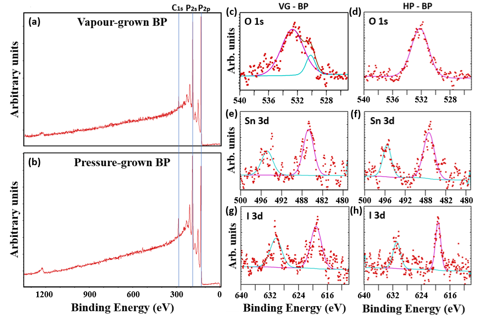
We use commercial BP samples obtained from two different suppliers: samples obtained from Smart-elements GmbH were fabricated using a vapour transport method 24, 25, while samples obtained from 2D Semiconductors Inc. were fabricated via a high pressure conversion of red phosphorus 26, 27. We refer to these samples as “vapour grown” and “high pressure” BP, respectively. To test for the presence of chemical impurities, we have analysed freshly cleaved samples of both sample types using XPS. Figures 2a,b show XPS survey scans for both sample types. All the major peaks in this scan belong to phosphorus with the only other feature being trace carbon contamination, likely due to low-level hydrocarbon background in the high-vacuum chamber used for the measurement. Additional contamination peaks (O, Sn, and I) were found using higher resolution and sensitivity XPS measurements, and we present these results in Figs. 2c–h. The presence of an oxygen peak at 532.5 eV for both samples (Figs. 2c,d) can be attributed to physisorbed water, since the samples were cleaved in ambient conditions before being immediately introduced to the vacuum chamber. The vapor grown sample (Fig. 2c) exhibits a smaller component at 530.2 eV, which may indicate some trace oxidation of the sample 28; this difference between the two samples can be attributed to the significantly smaller crystal sizes of vapour grown BP, producing a higher density of crystal edges and rendering the samples more vulnerable to oxidisation 29. Tin and iodine peaks were also found in both sample types (Figs. 2e–h). The observation of these elements in our samples is in agreement with a previous report 30 and can be attributed to the use of tin and iodine as catalysts during synthesis. Similar high resolution scans in other regions (e.g., Fe, Cu, Ti, Zn) did not produce any measurable peaks. It is notable that for both of our sample types the tin and iodine peaks are close to the measurement limit of our instrument.
3.2 DFT calculations of tin and iodine impurities in BP
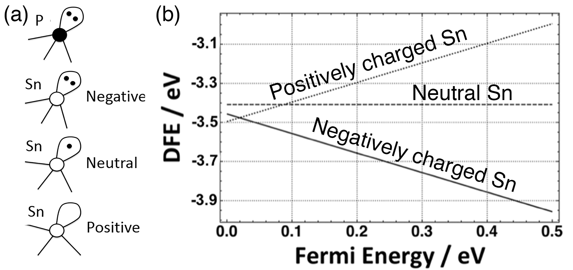
The observation of tin and iodine in our samples suggests the possibility that one or both of these impurity species is responsible for the p-type doping of BP and/or the observed long-range defect features seen in STM images. Recent DFT calculations examined a wide range of impurities in BP in adsorbed, intercalated, and substitutional lattice positions 17. Iodine was found to produce the least stable structures of all the elements considered. The most stable iodine structure was an adsorbed neutral iodine atom, which did not produce any electronic states in the BP bandgap 17. The absence of a localised charge or bandgap state rules out iodine being responsible for the features observed in STM images. In contrast, the substitutional tin impurity was found to be the most stable of all impurity defects considered 17. To better understand the defect behaviour as it is moved from the surface into the bulk, Sn impurities were calculated in various depths in a four layer BP slab. The slab consisted of 1296 atoms ( surface unit cell) and a single substitutional Sn was calculated in the upper row of the top layer, in the bottom row of the top layer and similarly in the second layer. As the Sn atom is moved into the slab the formation energy decreases slightly. The positively charged Sn in the top row of the top layer has the formation energy of -3.50 eV, while that in the second layer is slightly reduced to -3.56 eV.
To investigate whether substitutional tin impurities might be the cause of the p-type doping in BP and the features observed in STM images, it is necessary to determine the relative stability of the three possible charge states of the defect (negative, neutral, and positive) in the presence of an electron reservoir with a chemical potential equal to the Fermi level of the crystal. To achieve this, we calculate the formation energies of the positive and negative charge states of the substitutional tin impurity at the surface of the four layer slab by adding or subtracting a single electron from the computational cell 31. The resulting defect states are drawn schematically in Fig. 3a. Each phosphorus atom in BP is three-fold coordinated with an electron lone pair. Tin has one less valence electron than phosphorus, such that the neutral state of tin in BP features a singly-occupied dangling bond orbital. The negative charge state of the substitutional defect has one additional electron, forming a lone pair, while the positive charge state has one less electron than the neutral case, leaving an unoccupied dangling bond orbital on the tin atom. The relative stability of the three charge states as a function of the Fermi level, referenced to the valence band maximum, is ploted in Fig. 3(b). From this charge transition level plot, we see that the negative charge state of the substitutional tin impurity is energetically favourable for Fermi level values across most of the bandgap; the positively charged state is favourable only when the Fermi level lies within 0.02 eV of the valence band edge, and the neutral state is never favoured. This demonstrates that an isolated substitutional tin impurity in BP will naturally adopt a negatively charged configuration by capturing an electron from the BP conduction band. As the number of substitutional tin impurities increases, this will naturally lead to a shift of the Fermi level toward the valence band in an analogous manner to acceptor states in cubic semiconductors. The above results suggest that the p-type doping commonly observed in BP samples can be attributed to substitutional tin impurities.
3.3 Tunneling spectroscopy of surface defects
Next, we consider whether substitutional tin impurities can explain the long-ranged defect features commonly observed in STM images of BP. In cubic semiconductors, such as silicon and gallium arsenide, long-ranged features that appear superimposed on the surface atomic lattice have been attributed to presence of bulk substitutional dopant impurities located within several nanometres of the surface 32, 33, 34. Early reports found isotropic circular protrusions and depressions that were attributed to the effect of a localised charge-induced band bending, i.e., imaging the screened Coulomb potential of the dopant atom 32. Later reports discovered that in some cases it is also possible to find highly anisotropic protrusions, and these features have been attributed to directly imaging the probability distributions of the hydrogenic states of substitutional dopants 33, 34. The highly anisotropic, double-lobed protrusions that are seen in BP (Figs. 1b-d) are thus suggestive of imaging anisotropic hydrogenic states induced by a substitutional dopant.
To determine whether this is the case, we have performed tunnelling spectroscopy measurements on the defects. Figure 4a shows tunnelling spectroscopy measurements recorded over a defect-free area of the surface (black trace) and over a double-lobed feature (red trace). From the measurement over the defect free region we are able to extract a bandgap of eV, in agreement with previous reports 35, and we confirm that our sample is p-type 5, 6, 7, 8. Examining the STS measurement over the defect, we notice a bandgap state peak at eV, just above the valence band maximum. We also notice that the defect measurement shows a shoulder at eV, suggestive of a second peak deep within the bandgap. These features are consistent with previously published spectra of defects in BP 7.
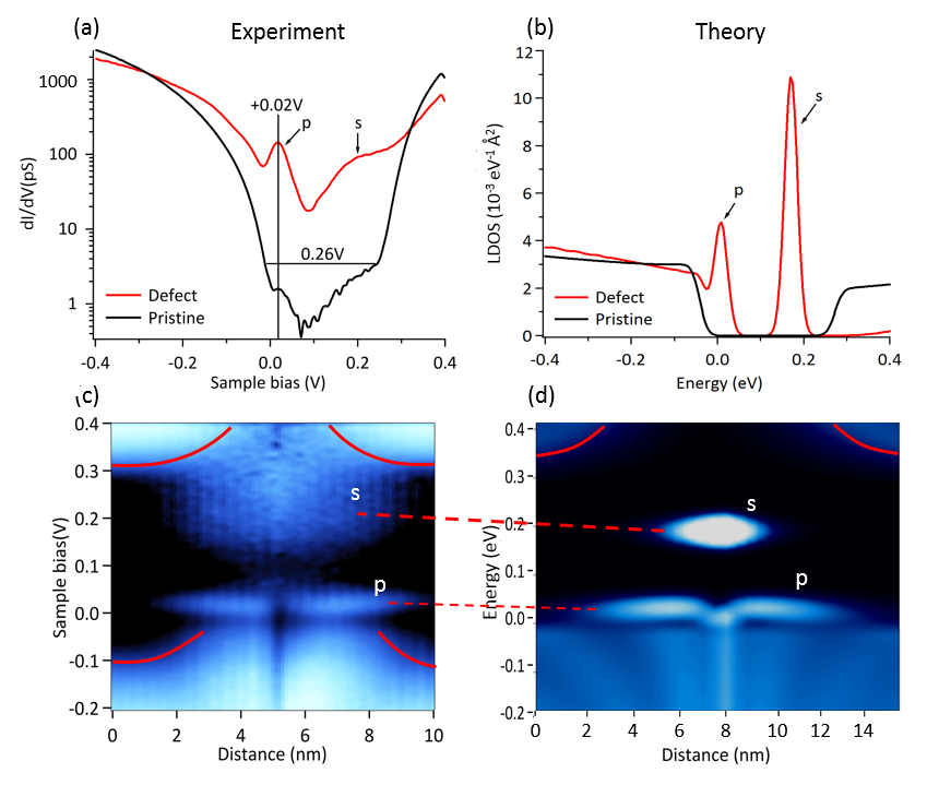
Figure 4c shows tunnelling spectrum as a function of position (horizontal axis) along the centre line of a single defect. The left and right regions (near 0 nm and 10 nm) show the spectrum acquired over the clean surface and are in agreement with the point spectroscopy measurements in Fig. 4a (black trace). The central region of the measurement, i.e., between and 8 nm, shows the spatial variation of the tunnelling spectroscopy along the length of the defect. In particular, the bandgap state that was seen at eV in the point spectrum (Fig. 4a) is resolved into a double-lobed feature with a node in the centre extending nm across the surface; this is the same spatial variation as the features observed in the topographic images, demonstrating that this bandgap state is the origin of the double-lobed features observed in STM images. The broad shoulder at eV appears as a diffuse region of enhanced conductivity, notably appearing as a continuous region with a maximum intensity near the centre rather than a node as in the case for the 0.02 eV feature. We do also see some upward band bending of the band edges on either side of the defect, consistent with the defect carrying a negative point charge.
3.4 Calculations of hydrogenic states of tin at the BP surface
In order to explain the physical characteristics of the defect state and determine whether it can be attributed to substitutional tin, it is necessary to perform simulations with unit cells large enough to model hydrogenic wave functions, and to capture the effects of charge-induced band bending. Such unit cells consist of many thousands of atoms, and are not currently accessible using DFT. Therefore, we have modelled the hydrogenic states produced by a substitutional tin impurity using tight-binding calculations. In these calculations, the defect is modelled as a negative point charge at the position of the tin nucleus (see Methods), which represents the negative charge that is localised on the lone pair orbital of the substutional tin impurity as predicted by our DFT calculations. We plot the simulated local density of states (LDOS) resulting from the tight-binding calculation in Fig. 4b; the red and black traces show the calculation with and without the negative point charge, respectively, and these can be compared directly to the corresponding experimentally measured tunnelling point spectra in Fig. 4a.
The simulated LDOS of the defect-free surface (black trace, Fig. 4b) reproduces the bandgap seen in the experimental data (black trace, Fig. 4a). The simulated LDOS of the defect (red trace, Fig. 4b) shows a bandgap state near the valence band maximum and a second peak near 0.18 eV, in good agreement with the experimental data (red trace, Fig. 4a). The spatial variation of the LDOS across a defect is shown in Fig. 4d and can be compared to the experimental measurement in Fig. 4c. Here we see that the double-lobed state just inside the bandgap at the valence band edge is reproduced in our tight bonding model, as is the upward band bending of the conduction band edge. The tight binding simulation also shows a nodeless state close to mid-gap, that corresponds well to the nodeless state observed in the experimental data.
The gap states in the tight-binding simulations are hydrogenic states induced by the localised negative point charge placed in the lattice to represent the negatively-charged substitutional tin impurity. This negative charge creates a partially screened Coulomb potential and induces hydrogenic defect states. Analysis of the simulation data shows that the two bandgap states in Fig. 4b can be attributed to the 1s hydrogenic ground state, and the 2px hydrogenic excited state (where corresponds to the heavy hole, i.e., armchair, direction), while the 2s and 2py states are shifted into the BP valence band. It is the anisotropic electronic structure of BP that results in the reordering of the state energies compared with the normal spherical hydrogenic model.
4 Conclusion
We have investigated the origin of p-type doping in nominally-intrinsic BP, and whether this doping can be attributed to the long-ranged defects commonly observed in STM images of BP. Using the combination of XPS, atomic-resolution STM/STS, and DFT, we demonstrated that tin impurities are present in BP samples, and that substitutional tin impurities are both highly stable and act as acceptor states. Using tight-binding calculations, we have demonstrated that substitutional tin impurities induce hydrogenic defect states in BP, and that the 2p state of these defects is the main source of the long-range features observed in STM images of BP. These observations provide compelling evidence that substitutional tin impurities are responsible for the p-type doping in BP, and are the origin of the long-ranged defect features observed in STM images of BP.
Acknowledgements
MW and MA were supported through studentships in the EPSRC Centre for Doctoral Training in Advanced Characterisation of Materials (EP/L015277/1) and EPSRC Centre for Doctoral Training in Theory and Simulation of Materials (EP/L015579/1), respectively. AAM, JL, ALS, MA, JG, and AJK acknowledge the support of the Thomas Young Centre through grant TYC-101. ALS and AJK acknowledge funding provided by EPSRC (EP/P013503/1), and Leverhulme Trust (RPG-2016-135). SRS acknowledges funding provided by EPSRC (EP/L002140/1). JG acknowledges the use of the ARCHER high-performance computing facilities via the membership in the U.K.s HPC Materials Chemistry Consortium, funded by EPSRC (EP/L000202) and the computer resources of the UK Materials and Molecular Modelling Hub, which is partially funded by EPSRC (EP/P020194).
References
- Kim et al. 2019 Kim, D. K.; Hong, S. B.; Jeong, K.; Lee, C.; Kim, H.; Cho, M. H. P-N Junction Diode Using Plasma Boron-Doped Black Phosphorus for High-Performance Photovoltaic Devices. ACS Nano 2019, 13, 1683–1693
- Jia et al. 2019 Jia, J.; Jeon, S.; Jeon, J.; Park, J. H.; Lee, S. Versatile Doping Control of Black Phosphorus and Functional Junction Structures. J. Phys. Chem. C 2019, 123, 10682–10688
- Novoselov et al. 2004 Novoselov, K. S.; Geim, A. K.; Morozov, S. V.; Jiang, D.; Zhang, Y.; Dubonos, S. V.; Grigorieva, I. V.; Firsov, A. A. Electric Field Effect in Atomically Thin Carbon Films. Science 2004, 306, 666–669
- Warschauer 1963 Warschauer, D. Electrical and optical properties of crystalline black phosphorus. J. Appl. Phys. 1963, 34, 1853–1860
- Akahama et al. 1983 Akahama, Y.; Endo, S.; Narita, S.-i. Electrical Properties of Black Phosphorus Single Crystals. Journal of the Physical Society of Japan 1983, 52, 2148–2155
- Castellanos-Gomez 2015 Castellanos-Gomez, A. Black Phosphorus: Narrow Gap, Wide Applications. Journal of Physical Chemistry Letters 2015, 6, 4280–4291
- Kiraly et al. 2017 Kiraly, B.; Hauptmann, N.; Rudenko, A. N.; Katsnelson, M. I.; Khajetoorians, A. A. Probing Single Vacancies in Black Phosphorus at the Atomic Level. Nano Letters 2017, 17, 3607–3612
- Qiu et al. 2017 Qiu, Z.; Fang, H.; Carvalho, A.; Rodin, A. S.; Liu, Y.; Tan, S. J.; Telychko, M.; Lv, P.; Su, J.; Wang, Y. et al. Resolving the Spatial Structures of Bound Hole States in Black Phosphorus. Nano Letters 2017, 17, 6935–6940
- Li et al. 2012 Li, L.; Lu, W.; Zhu, X.; Sun, Y. Effect of Fe-doping on charge density wave in 1T-TaS2: Instability and induced superconductivity. Journal of Physics: Conference Series 2012, 400, 022061
- McChesney et al. 2010 McChesney, J. L.; Bostwick, A.; Ohta, T.; Seyller, T.; Horn, K.; González, J.; Rotenberg, E. Extended van Hove Singularity and Superconducting Instability in Doped Graphene. Phys. Rev. Lett. 2010, 104, 136803
- Xia et al. 2014 Xia, F.; Wang, H.; Jia, Y. Rediscovering black phosphorus as an anisotropic layered material for optoelectronics and electronics. Nat. Commun. 2014, 5, 4458
- Rodin et al. 2014 Rodin, A. S.; Carvalho, A.; Castro Neto, A. H. Strain-Induced Gap Modification in Black Phosphorus. Phys. Rev. Lett. 2014, 112, 176801
- Zhang et al. 2009 Zhang, C. D.; Lian, J. C.; Yi, W.; Jiang, Y. H.; Liu, L. W.; Hu, H.; Xiao, W. D.; Du, S. X.; Sun, L. L.; Gao, H. J. Surface Structures of Black Phosphorus Investigated with Scanning Tunneling Microscopy. The Journal of Physical Chemistry C 2009, 113, 18823–18826
- Riffle et al. 2018 Riffle, J. V.; Flynn, C.; St Laurent, B.; Ayotte, C. A.; Caputo, C. A.; Hollen, S. M. Impact of vacancies on electronic properties of black phosphorus probed by STM. Journal of Applied Physics 2018, 123
- Guo and Robertson 2015 Guo, Y.; Robertson, J. Vacancy and Doping States in Monolayer and bulk Black Phosphorus. Sci.Rep 2015, 1–10
- Cai et al. 2016 Cai, Y.; Ke, Q.; Zhang, G.; Yakobson, B. I.; Zhang, Y. W. Highly Itinerant Atomic Vacancies in Phosphorene. JACS 2016, 138, 10199–10206
- Gaberle and Shluger 2018 Gaberle, J.; Shluger, A. L. Structure and Properties of Intrinsic and Extrinsic Defects in Black Phosphorus. Nanoscale 2018, 10, 19536–19546
- Hu and Dong 2015 Hu, T.; Dong, J. Geometric and electronic structures of mono- and di-vacancies in phosphorene. Nanotechnology 2015, 26, 0–9
- VandeVondele et al. 2005 VandeVondele, J.; Krack, M.; Mohamed, F.; Parrinello, M.; Chassaing, T.; Hutter, J. Quickstep: Fast and Accurate Density Functional Calculations Using a Mixed Gaussian and Plane Waves Approach. Comp. Phys. Commun. 2005, 167, 103–128
- VandeVondele and Hutter 2007 VandeVondele, J.; Hutter, J. Gaussian Basis Sets for Accurate Calculations on Molecular Systems in Gas and Condensed Phases. J. Chem. Phys. 2007, 127, 114105–1–9
- Guidon et al. 2009 Guidon, M.; Hutter, J.; VandeVondele, J. Robust Periodic Hartree Fock Exchange for Large-Scale Simulations Using Gaussian Basis Sets. J. Chem. Theory Comput. 2009, 5, 3010–3021
- Guidon et al. 2010 Guidon, M.; Hutter, J.; VandeVondele, J. Auxiliary Density Matrix Methods for Hartree Fock Exchange Calculations. Journal of Chemical Theory and Computation 2010, 6, 2348–2364
- Rudenko and Katsnelson 2014 Rudenko, A. N.; Katsnelson, M. I. Quasiparticle band structure and tight-binding model for single- and bilayer black phosphorus. Phys. Rev. B 2014, 89, 1–6
- Lange et al. 2007 Lange, S.; Schmidt, P.; Nilges, T. Au3SnP7 Black Phosphorus: An Easy Access to Black Phosphorus. Inorganic Chemistry 2007, 46, 4028–4035
- Köpf et al. 2014 Köpf, M.; Eckstein, N.; Pfister, D.; Grotz, C.; Krüger, I.; Greiwe, M.; Hansen, T.; Kohlmann, H.; Nilges, T. Access and in situ growth of phosphorene-precursor black phosphorus. Journal of Crystal Growth 2014, 405, 6–10
- Bridgman 1914 Bridgman, P. W. Two New Modifications of Phosphorus. JACS 1914, 36, 1344–1363
- Shirotani 1982 Shirotani, I. Growth of Large Single Crystals of Black Phosphorus at High Pressures and Temperatures, and its Electrical Properties. Molecular Crystals and Liquid Crystals 1982, 86, 203–211
- Luo et al. 2016 Luo, W.; Zemlyanov, D. Y.; Milligan, C. A.; Du, Y.; Yang, L.; Wu, Y.; Ye, P. D. Surface chemistry of black phosphorus under a controlled oxidative environment. Nanotechnology 2016, 27, 434002
- Kuntz et al. 2017 Kuntz, K. L.; Wells, R. A.; Hu, J.; Yang, T.; Dong, B.; Guo, H.; Woomer, A. H.; Druffel, D. L.; Alabanza, A.; Tomanek, D. et al. Control of Surface and Edge Oxidation on Phosphorene. ACS Applied Materials & Interfaces 2017, 9, 9126–9135
- Mayorga-Martinez et al. 2018 Mayorga-Martinez, C. C.; Sofer, Z.; Sedmidubský, D.; Luxa, J.; Kherzi, B.; Pumera, M. Metallic impurities in black phosphorus nanoflakes prepared by different synthetic routes. Nanoscale 2018, 10, 1540–1546
- Schofield et al. 2013 Schofield, S. R.; Studer, P.; Hirjibehedin, C. F.; Curson, N. J.; Aeppli, G.; Bowler, D. R. Quantum engineering at the silicon surface using dangling bonds. Nat. Commun. 2013, 4, 1649
- Liu et al. 2001 Liu, L.; Yu, J.; Lyding, J. W. Atom-resolved three-dimensional mapping of boron dopants in Si(100) by scanning tunneling microscopy. Appl. Phys. Lett. 2001, 78, 386
- Yakunin et al. 2004 Yakunin, a.; Silov, A.; Koenraad, P. M.; Wolter, J.; Van Roy, W.; De Boeck, J.; Tang, J.-M.; Flatté, M. Spatial Structure of an Individual Mn Acceptor in GaAs. Phys. Rev. Lett. 2004, 92, 216806
- Sinthiptharakoon et al. 2014 Sinthiptharakoon, K.; Schofield, S. R.; Studer, P.; Brázdová, V.; Hirjibehedin, C. F.; Bowler, D. R.; Curson, N. J. Investigating individual arsenic dopant atoms in silicon using low-temperature scanning tunnelling microscopy. J. Phys. Condens. Matter 2014, 26, 012001
- Prytz and Flage-Larsen 2010 Prytz, O.; Flage-Larsen, E. The Influence of Exact Exchange Corrections in van der Waals Layered Narrow Bandgap Black Phosphorus. J. Phys: Condens. Matter 2010, 22, 015502