Design Technology Co-Optimization for Neuromorphic Computing
Abstract
We present a design-technology tradeoff analysis in implementing machine-learning inference on the processing cores of a Non-Volatile Memory (NVM)-based many-core neuromorphic hardware. Through detailed circuit-level simulations for scaled process technology nodes, we show the negative impact of design scaling on read endurance of NVMs, which directly impacts their inference lifetime. At a finer granularity, the inference lifetime of a core depends on 1) the resistance state of synaptic weights programmed on the core (design) and 2) the voltage variation inside the core that is introduced by the parasitic components on current paths (technology). We show that such design and technology characteristics can be incorporated in a design flow to significantly improve the inference lifetime.
I Introduction
Neuromorphic systems are integrated circuits designed to mimic the computations in a mammalian brain [1]. They enable energy-efficient execution of Spiking Neural Networks (SNN) [2] and therefore, these systems are suitable for implementing machine learning inference tasks for embedded Systems and Edge devices in Internet-of-Things (IoT). A neuromorphic system consists of processing cores that implement neurons and synapses. Multiple such cores are interconnected together using Segmented Bus [3] or Network-on-Chip (NoC) [4] to design a many-core neuromorphic hardware [5]. Table I illustrates the neuron and synapse capacity of recent neuromorphic hardware cores.
| ODIN | Brain | DYNAPs | BrainScaleS | SpiNNaker | Neurogrid | Loihi | TrueNorth | |
| [6] | [7] | [8] | [9] | [10] | [11] | [12] | [13] | |
| # Neurons/core | 256 | 336 | 256 | 512 | 36K | 65K | 130K | 1M |
| # Synapses/core | 64K | 38K | 16K | 128K | 2.8M | 8M | 130M | 256M |
| # Cores/chip | 1 | 1 | 1 | 1 | 144 | 128 | 128 | 4096 |
| # Chips/board | 1 | 1 | 4 | 352 | 56 | 16 | 768 | 4096 |
| # Neurons | 256 | 336 | 1K | 4M | 2.5B | 1M | 100M | 4B |
| # Synapses | 256 | 336 | 65K | 1B | 200B | 16B | 100B | 1T |
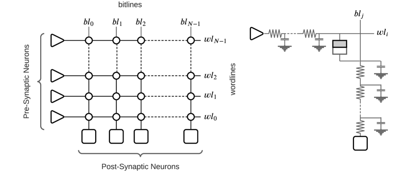
A neuromorphic core can be implemented using an analog crossbar where bitlines and wordlines are organized in a grid with memory cells connected at their crosspoints to store the synaptic weights [14, 15, 16, 17]. Neuron circuits are implemented along bitlines and wordlines (see Figure 2). Recently, Non-Volatile Memory (NVM) technologies such as phase-change memory (PCM) and oxide-based resistive switching random access memory (OxRRAM) are used to implement the memory cells in a neuromorphic core due to their low power consumption, CMOS-compatible scaling, and multilevel analog operations [18].111NVMs are also used in classical von Neumann computing to mitigate the performance and energy bottlenect of DRAM [19, 20, 21, 22, 23, 24, 25]. In an NVM-based neuromorphic inference hardware, the resistance state corresponding to the synaptic weights of an SNN are programmed on the NVM cells.
Unfortunately, NVMs suffer from reliability issues such as circuit aging, limited endurance, and read disturbance [26, 27, 28, 29]. Many of these issues have been addressed recently in the context of neuromorphic computing [30, 31, 32, 33, 34, 35, 36, 37]. In this work, we focus on the read disturbance issues of OxRRAM technology, where an OxRRAM cell’s resistance state may change after performing a certain number of read operations [38, 39, 40]. Therefore, when an OxRRAM-based neuromorphic hardware is used to implement an inference task, the trained synaptic weights programmed on the hardware may change after performing a few inference operations. To ensure expected results from an inference task, the trained weights need to be reprogrammed on to the hardware periodically. Reprogramming of synaptic weights to a neuromorphic hardware involves offlining the hardware and transferring the weights from the host to the hardware via a bandwidth-limited interconnect. This can significantly increase the overhead, and lower the availability and reliability of neuromorphic computing.
In this work, we present a design-technology tradeoff analysis in implementing machine learning inference on many-core neuromorphic hardware. Through circuit-level simulations we show the negative impact of design scaling on read endurance of NVMs, which directly impacts their inference lifetime. We show that the inference lifetime of a crossbar depends on 1) the resistance state of synaptic weights programmed on the NVMs and 2) the voltage variation inside the crossbar that is introduced by the parasitic components on current paths. Such design and technology characteristics can be incorporated in a design flow to significantly improve the inference lifetime.
II Background
We briefly introduce Spiking Neural Network (SNN) and their implementation in hardware.
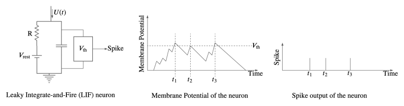
Spiking Neural Networks (SNNs) are the third generation of neural networks designed using spiking neurons and bio-inspired learning algorithms [2]. In an SNN, spikes injected from pre-synaptic neurons raise the membrane voltage of a post-synaptic neuron (middle sub-figure of Figure 1). When the membrane voltage crosses a threshold (), the post-synaptic neuron emits spikes that propagate to other neurons (right sub-figure of Figure 1). SNNs implement some variants of Integrate and Fire (I&F) neurons with a spike duration ranging from 1 s to several ms [41, 42, 43] (left sub-figure of Figure 1).
SNNs can implement many machine learning approaches [44, 45, 46, 47, 48, 49, 50, 51]. In a supervised machine learning, an SNN is pre-trained with representative data. Machine-learning inference refers to feeding live data points to this trained SNN to generate the corresponding output. The quality of machine learning inference can be expressed in terms of accuracy [48], Mean Square Error (MSE) [44], Peak Signal-to-Noise Ratio (PSNR) [52], and Structural Similarity Index Measure (SSIM) [53]. For SNNs, these quality metrics are defined in terms of the inter-spike interval (ISI) [54, 55, 56, 57]. If denote a neuron’s firing times in the time interval , the average ISI of this spike train is
| (1) |
A neuromorphic hardware platform is implemented as a tiled architecture, where tiles are interconnected via a time-multiplexed shared interconnect. Each tile consists of a neuromorphic processing core, which can implement neurons and synapses of a machine learning model. A common design practice is to use an analog crossbar to implement a core.
In a crossbar, pre-synaptic neuron circuits are placed on horizontal wires called wordlines, while post-synaptic neuron circuits are placed on vertical wires called bitlines. Memory cells are placed at the crosspoint of each wordline and bitline, and they implement the synaptic weights of an SNN. The left subfigure of Figure 2 illustrates an crossbar. The right subfigure illustrates the parasitic RC components on the current path from a pre-synaptic neuron to a post-synaptic neuron accessing the memory cell located at the crosspoint of wordline and bitline.
Overall, a neuromorphic hardware enables distributed and pipelined processing of SNN operations. Additionally, each crossbar in the hardware can implement a maximum of pre-synaptic neurons per post-synaptic neuron. Therefore, system-software frameworks such as NEUTRAMS [58], NeuroXplorer [59], Corelet [60], PACMAN [61], and LAVA [62] consist of 1) a compiler, which partitions an SNN model into clusters such that the neurons and synapses of each cluster can be mapped to a crossbar of the hardware, and 2) a run-time manager, which maps the clusters of an SNN to the cores of a many-core hardware. To this end, several mapping strategies have been proposed, including optimizing for energy [63, 64, 65, 66], throughput [67, 68, 69, 70], resource utilization [71, 72, 62, 58, 56], circuit aging [34, 31, 32, 30, 33], inference lifetime [39], and write endurance [35, 36, 37]. These mapping techniques all use some variant of the SNN-partitioning approach proposed in SpiNeMap [64].
Recently, dataflow models have been used to analyze performance of SNNs implemented on neuromorphic hardware, especially using Synchronous Dataflow Graphs (SDFGs) [73].222SDFGs are commonly used to model streaming applications that are implemented on a multi-core system and their performance analysis [74, 75, 76, 77, 78]. There are two strategies proposed in literature – the SDFSNN [67] and its extended versions [68, 79, 80], which uses dataflow graphs to model an SNN, performing partitioning and mapping explorations with neurons and synapses directly, and the DFSynthesizer [69] and its extended version [70], which uses dataflow graphs to only model the clustered SNN, allowing mapping and scheduling of the clusters (a collection of neurons and synapses) to the PEs of a neuromorphic hardware.
Emerging non-volatile memory (NVM) technologies such as phase-change memory (PCM), oxide-based memory (OxRAM), spin-based magnetic memory (STT-MRAM), and Flash have recently been used for synaptic storage in crossbars. NVMs are non-volatile, have high CMOS compatibility, and can achieve high integration density. Each NVM device can implement both a single-bit and multi-bit synapse. Because of these properties, an NVM-based neuromorphic hardware typically consumes energy that is magnitudes lower than using SRAMs [81, 82, 83]. However, NVMs also introduce reliability issues [26]. Table II summarizes them for different NVMs.
| Reliability Issues | NVMs |
|---|---|
| High-voltage related circuit aging | PCM, Flash |
| High-current related circuit aging | OxRAM, STT-MRAM |
| Limited read endurance | All |
| Limited write endurance | All |
We discuss one specific issue – limited read endurance for OxRRAM-based neuromorphic hardware.
III Introduction to Oxide-based Resistive RAM
The resistance switching random access memory (OxRRAM) technology presents an attractive option for implementing the synaptic cells of a crossbar due to its demonstrated potential for low-power multi-level operation and high integration density [18]. An OxRRAM cell is composed of an insulating film sandwiched between conducting electrodes forming a metal-insulator-metal (MIM) structure (see Figure 3). Recently, filament-based metal-oxide OxRRAM implemented with transition-metal-oxides such as HfO2, ZrO2, and TiO2 has received considerable attention due to their low-power and CMOS-compatible scaling.
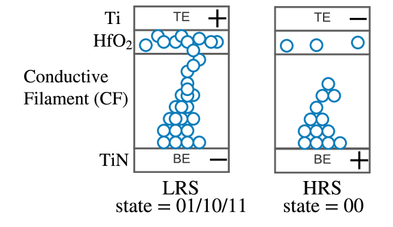
Synaptic weights are represented as conductance of the insulating layer within each OxRRAM cell. To program an OxRRAM cell, elevated voltages are applied at the top and bottom electrodes, which re-arranges the atomic structure of the insulating layer. Figure 3 shows the High-Resistance State (HRS) and the Low-Resistance State (LRS) of an OxRRAM cell. An OxRRAM cell can also be programmed into intermediate low-resistance states, allowing its multilevel operations.
In OxRRAM technology, the transition from HRS state is governed by a sudden decrease of the vertical filament gap on application of stress voltage during spike propagation [38]. This is illustrated in the left subfigure of Figure 4 where the vertical filament gap is shown to reduce by an amount . This may result in a conducting filament between the two metal layers causing the resistive state to change from HRS to LRS. The rate of change of the filament gap of the OxRRAM cell at the location in the crossbar is
| (2) |
In the above equation, defines the state transition time, is the initial filament gap of the OxRRAM cell, is the voltage applied to the cell, is the local field enhancement factor and is related to the gap , is the atomic hoping distance, and is a fitting constant.
The transition from one of the LRS states is governed by the lateral filament growth [38]. This is illustrated in the right subfigure of Figure 4. The time for state transition in the RRAM cell is given by
| (3) |
If the state transition time of an OxRRAM cell is 1000 ms, then a single quasi-static read operating using 1000 ms read pulse or 1000 read accesses using with 1-ms spike pulses can lead to an abrupt change in the state of the cell. Therefore, the endurance of the cell is 1000. If the cell propagates spikes during inference of each image, then the inference lifetime is defined as . Formally,
| (4) |
IV Design-Technology Tradeoff Analysis
The computer memory industry has thus far been primarily driven by the cost-per-bit metric, which provides the maximum capacity for a given manufacturing cost. As shown in recent works [22, 21, 84, 19, 20, 23, 24], manufacturing cost can be estimated from the area overhead. To estimate the cost-per-bit of a neuromorphic core, we investigate the internal architecture of a crossbar and find that a neuron circuit can be designed using 20 transistors and a capacitor [85], while an NVM cell is a 1T-1R arrangement with a transistor used as an access device for the cell. Within an crossbar, there are pre-synaptic neurons, post-synaptic neurons, and synaptic cells. The total area of all the neurons and synapses of a crossbar is
| neuron area | ||||
| synapse area |
where stands for transistor, for capacitor, and for NVM cell. The total synaptic cell capacity is , with each NVM cell implementing 2-bit per synapse. The total number of bits (i.e., synaptic capacity) in the crossbar is
| (6) |
Therefore, the cost-per-bit of an x crossbar is
| (7) |
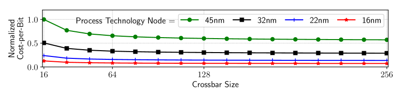
where the cost-per-bit is represented in terms of the crossbar dimension and the feature size . Equation 7 provides a back-of-the-envelope calculation of cost-per-bit. Figure 5 plots the normalized cost-per-bit for four different process technology nodes, with the crossbar dimension ranging from 16 to 256. We observe that the cost-per-bit reduces with increase in the dimension of a crossbar, i.e., larger-sized crossbars can accommodate more bits for a given cost.
We now analyze the internal architecture of a crossbar. Figure 6a shows the current through the memory cells in a 128x128 crossbar. This current variation is due to the difference in the length of current paths from pre to post-synaptic neurons in the crossbar, where the length of a current path is measured in terms of the number of parasitic components on the path. These current values are obtained for a 65nm technology node and at 300K temperature corner. As can be clearly seen from the figure, current through memory cells on the top-right corner of the crossbar is lower than those at the bottom-left corner.
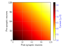
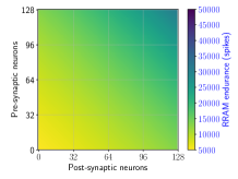
Figure 6b shows the endurance variation of a 128x128 crossbar at 45 nm node and at 30∘C with each RRAM cell programmed to HRS state. The endurance variation is a direct result of the current variation in the crossbar.
Figure 7 shows the difference between currents on the shortest and longest paths for 32x32, 64x64, 128x128, and 256x256 crossbars at 65nm process node. The input spike voltage of the pre-synaptic neurons is set to generate on the longest path. This current value corresponds to the current needed to read the resistance state of an OxRRAM cell.
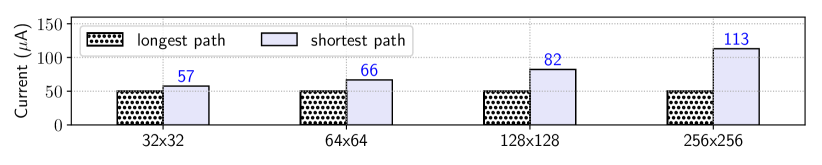
We observe that the current injected into the post-synaptic neuron on the longest path is lower than the current on the shortest path by 13.3% for 32x32, 25.1% for 64x64, 39.2% for 128x128, and 55.8% for 256x256 crossbar. This current difference is because of the higher voltage drop on the longest path, which reduces the current on this path compared to the shortest path for the same amount of spike voltage applied on both these paths. The current difference increases with crossbar size because of the increase in the number of parasitic resistances on the longest current path, which results in larger voltage drops, lowering the current injected into its post-synaptic neuron. However, larger current variation causes larger endurance variation as illustrated in Figure 6b. Therefore, larger crossbar sizes leads to larger endurance variation.
System designers often make a tradeoff between cost-per-bit and endurance variation. Typically, crossbar sizes of and gives the best tradeoff.
V Design Flow Incorporating
Design-Technology Tradeoff
An optimized design flow is one, which takes into account the design and technology characteristics to place neurons and synapses to a crossbar such that those synapses that propagate more spikes are mapped to NVMs with higher read endurance. This is to increase the inference lifetime.
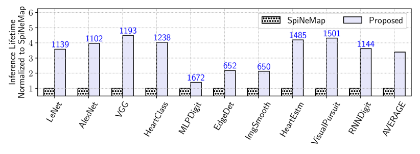
In our prior work [39], we show that such a design flow can significantly improve the inference lifetime. Figure 8 reports the inference lifetime for 10 applications for the proposed design flow normalized to SpiNeMap. We observe that through intelligent synapse mapping, the inference lifetime obtained using the proposed approach is on average 3.4x higher.
VI Conclusion
A design-technology tradeoff analysis is performed to investigate inference lifetime of neuromorphic hardware that adopts NVM as synaptic storage. An essential observation of the analysis is that the read endurance of an NVM cell depends on its programmed synaptic weight (design) and the voltage exposed to the cell (technology). Our analysis also reveals that voltages exposed to NVM cells inside a crossbar vary due to the parasitic components on current paths, which leads to asymmetric read endurance across NVM cells in a crossbar. From detailed circuit-level simulations, we show design scaling on read endurance of NVMs negatively impacts the inference lifetime of neuromorphic hardware. In addition, the design flow that considers asymmetry in read endurance can significantly improve the inference lifetime of neuromorphic hardware.
Acknowledgment
This work is supported by the United States National Science Foundation Faculty Early Career Development Award CCF-1942697 (CAREER: Facilitating Dependable Neuromorphic Computing: Vision, Architecture, and Impact on Programmability) and the United States Department of Energy CAREER Award DE-SC0022014 (Architecting the Hardware-Software Interface for Neuromorphic Computers).
References
- [1] C. Mead, “Neuromorphic electronic systems,” Proc. of the IEEE, 1990.
- [2] W. Maass, “Networks of spiking neurons: The third generation of neural network models,” Neural Networks, 1997.
- [3] A. Balaji et al., “Exploration of segmented bus as scalable global interconnect for neuromorphic computing,” in GLSVLSI, 2019.
- [4] X. Liu et al., “Neu-NoC: A high-efficient interconnection network for accelerated neuromorphic systems,” in ASP-DAC, 2018.
- [5] F. Catthoor et al., “Very large-scale neuromorphic systems for biological signal processing,” in CMOS Circuits for Biological Sensing and Processing, 2018.
- [6] C. Frenkel et al., “A 0.086-mm2 12.7-pj/sop 64k-synapse 256-neuron online-learning digital spiking neuromorphic processor in 28-nm CMOS,” TBCAS, 2018.
- [7] J. Stuijt et al., “Brain: An event-driven and fully synthesizable architecture for spiking neural networks,” Frontiers in Neuroscience, 2021.
- [8] S. Moradi et al., “A scalable multicore architecture with heterogeneous memory structures for dynamic neuromorphic asynchronous processors (DYNAPs),” TBCAS, 2017.
- [9] J. Schemmel et al., “Live demonstration: A scaled-down version of the brainscales wafer-scale neuromorphic system,” in ISCAS, 2012.
- [10] S. Furber et al., “The SpiNNaker project,” Proc. of the IEEE, 2014.
- [11] B. Benjamin et al., “Neurogrid: A mixed-analog-digital multichip system for large-scale neural simulations,” Proceedings of the IEEE, 2014.
- [12] M. Davies et al., “Loihi: A neuromorphic manycore processor with on-chip learning,” IEEE Micro, 2018.
- [13] M. V. Debole et al., “TrueNorth: Accelerating from zero to 64 million neurons in 10 years,” Computer, 2019.
- [14] C. Liu et al., “A spiking neuromorphic design with resistive crossbar,” in DAC, 2015.
- [15] M. Hu et al., “Memristor crossbar-based neuromorphic computing system: A case study,” TNNLS, 2014.
- [16] M. Hu et al., “Dot-product engine for neuromorphic computing: Programming 1T1M crossbar to accelerate matrix-vector multiplication,” in DAC, 2016.
- [17] A. Ankit et al., “TraNNsformer: Neural network transformation for memristive crossbar based neuromorphic system design,” in ICCAD, 2017.
- [18] A. Mallik et al., “Design-technology co-optimization for OxRRAM-based synaptic processing unit,” in VLSIT, 2017.
- [19] S. Song et al., “Enabling and exploiting partition-level parallelism (PALP) in phase change memories,” TECS, 2019.
- [20] O. Mutlu, “Memory scaling: A systems architecture perspective,” in IMW, 2013.
- [21] S. Song et al., “Improving phase change memory performance with data content aware access,” in ISMM, 2020.
- [22] O. Mutlu et al., “Research problems and opportunities in memory systems,” SUFI, 2015.
- [23] S. Song et al., “Exploiting inter- and intra-memory asymmetries for data mapping in hybrid tiered-memories,” in ISMM, 2020.
- [24] S. Song et al., “Aging-aware request scheduling for non-volatile main memory,” in ASP-DAC, 2021.
- [25] S. Song et al., “Design methodologies for reliable and energy-efficient PCM systems,” in IGSC Workshops, 2020.
- [26] R. M. Shelby et al., “Non-volatile memory as hardware synapse in neuromorphic computing: A first look at reliability issues,” in IRPS, 2015.
- [27] L. Larcher et al., “High- related reliability issues in advanced non-volatile memories,” Microelectronics Reliability, 2010.
- [28] C.-Y. Lu et al., “Non-volatile memory technology-today and tomorrow,” in IPFA, 2006.
- [29] P. Noé et al., “Phase-change materials for non-volatile memory devices: from technological challenges to materials science issues,” Semiconductor Science and Technology, 2017.
- [30] S. Song et al., “A case for lifetime reliability-aware neuromorphic computing,” in MWSCAS, 2020.
- [31] A. Balaji et al., “A framework to explore workload-specific performance and lifetime trade-offs in neuromorphic computing,” CAL, 2019.
- [32] S. Song et al., “Improving dependability of neuromorphic computing with non-volatile memory,” in EDCC, 2020.
- [33] S. Kundu et al., “Special session: Reliability analysis for ML/AI hardware,” in VTS, 2021.
- [34] S. Song et al., “Dynamic reliability management in neuromorphic computing,” JETC, 2021.
- [35] T. Titirsha et al., “Reliability-performance trade-offs in neuromorphic computing,” in IGSC Workshops, 2020.
- [36] T. Titirsha et al., “Thermal-aware compilation of spiking neural networks to neuromorphic hardware,” in LCPC, 2020.
- [37] T. Titirsha et al., “Endurance-aware mapping of spiking neural networks to neuromorphic hardware,” TPDS, 2021.
- [38] W. Shim et al., “Impact of read disturb on multilevel RRAM based inference engine: Experiments and model prediction,” in IRPS, 2020.
- [39] S. Song et al., “Improving inference lifetime of neuromorphic systems via intelligent synapse mapping,” in ASAP, 2021.
- [40] K.-T. Chen et al., “Non-volatile ferroelectric FETs using 5-nm Hf 0.5 Zr 0.5 O 2 with high data retention and read endurance for 1T memory applications,” EDL, 2019.
- [41] S. Fusi et al., “Collective behavior of networks with linear (VLSI) integrate-and-fire neurons,” Neural Computation, 1999.
- [42] S. Zhang et al., “A pulse-width modulation neuron with continuous activation for processing-in-memory engines,” in DATE. IEEE, 2020.
- [43] A. J. Leigh et al., “An efficient spiking neuron hardware system based on the hardware-oriented modified Izhikevich neuron (HOMIN) model,” TCAS II: Express Briefs, 2020.
- [44] A. Das et al., “Unsupervised heart-rate estimation in wearables with Liquid states and a probabilistic readout,” Neural Networks, 2018.
- [45] E. J. Moyer et al., “Machine learning applications to DNA subsequence and restriction site analysis,” in SPMB, 2020.
- [46] J. P. Dominguez-Morales et al., “Deep spiking neural network model for time-variant signals classification: a real-time speech recognition approach,” in IJCNN, 2018.
- [47] A. Das et al., “Heartbeat classification in wearables using multi-layer perceptron and time-frequency joint distribution of ECG,” in CHASE, 2018.
- [48] A. Balaji et al., “Power-accuracy trade-offs for heartbeat classification on neural networks hardware,” JOLPE, 2018.
- [49] Q. Yu et al., “A spiking neural network system for robust sequence recognition,” TNNLS, 2015.
- [50] S. Schliebs et al., “Evolving spiking neural network—a survey,” Evolving Systems, 2013.
- [51] M. Dong et al., “Unsupervised speech recognition through spike-timing-dependent plasticity in a convolutional spiking neural network,” PloS one, 2018.
- [52] T. Chou et al., “CARLsim 4: An open source library for large scale, biologically detailed spiking neural network simulation using heterogeneous clusters,” in IJCNN, 2018.
- [53] A. Hore et al., “Image quality metrics: PSNR vs. SSIM,” in ICPR, 2010.
- [54] P. A. Cariani, “Temporal coding of sensory information in the brain,” Acoustical Science and Technology, 2001.
- [55] H. Fang et al., “Encoding, model, and architecture: systematic optimization for spiking neural network in FPGAs,” in ICCAD, 2020.
- [56] A. Balaji et al., “PyCARL: A PyNN interface for hardware-software co-simulation of spiking neural network,” in IJCNN, 2020.
- [57] M. Kiselev, “Rate coding vs. temporal coding-is optimum between?” in IJCNN, 2016.
- [58] Y. Ji et al., “NEUTRAMS: Neural network transformation and co-design under neuromorphic hardware constraints,” in MICRO, 2016.
- [59] A. Balaji et al., “NeuroXplorer 1.0: An extensible framework for architectural exploration with spiking neural networks,” in ICONS, 2021.
- [60] A. Amir et al., “Cognitive computing programming paradigm: a corelet language for composing networks of neurosynaptic cores,” in IJCNN, 2013.
- [61] F. Galluppi et al., “A hierachical configuration system for a massively parallel neural hardware platform,” in CF, 2012.
- [62] C.-K. Lin et al., “Mapping spiking neural networks onto a manycore neuromorphic architecture,” in PLDI, 2018.
- [63] A. Das et al., “Mapping of local and global synapses on spiking neuromorphic hardware,” in DATE, 2018.
- [64] A. Balaji et al., “Mapping spiking neural networks to neuromorphic hardware,” TVLSI, 2020.
- [65] T. Titirsha et al., “On the role of system software in energy management of neuromorphic computing,” in CF, 2021.
- [66] A. Balaji et al., “Run-time mapping of spiking neural networks to neuromorphic hardware,” JSPS, 2020.
- [67] A. Das et al., “Dataflow-based mapping of spiking neural networks on neuromorphic hardware,” in GLSVLSI, 2018.
- [68] A. Balaji et al., “A framework for the analysis of throughput-constraints of SNNs on neuromorphic hardware,” in ISVLSI, 2019.
- [69] S. Song et al., “Compiling spiking neural networks to neuromorphic hardware,” in LCTES, 2020.
- [70] S. Song et al., “DFSynthesizer: Dataflow-based synthesis of spiking neural networks to neuromorphic hardware,” TECS, 2021.
- [71] A. Balaji et al., “Enabling resource-aware mapping of spiking neural networks via spatial decomposition,” ESL, 2020.
- [72] A. Balaji et al., “Compiling spiking neural networks to mitigate neuromorphic hardware constraints”,” in IGSC Workshops, 2020.
- [73] E. Lee et al., “Synchronous data flow,” Proceedings of the IEEE, 1987.
- [74] S. Sriram et al., Embedded Multiprocessors; Scheduling and Synchronization, 2000.
- [75] L. Jiashu et al., “A design flow for partially reconfigurable heterogeneous multi-processor platforms,” in RSP, 2012.
- [76] A. Das et al., Reliable and Energy Efficient Streaming Multiprocessor Systems. Springer, 2018.
- [77] A. Das et al., “Reliability and energy-aware mapping and scheduling of multimedia applications on multiprocessor systems,” TPDS, 2015.
- [78] A. H. Ghamarian et al., “Throughput analysis of synchronous data flow graphs,” in ACSD, 2006.
- [79] S. Song et al., “A design flow for mapping spiking neural networks to many-core neuromorphic hardware,” in ICCAD, 2021.
- [80] S. Curzel et al., “Automated generation of integrated digital and spiking neuromorphic machine learning accelerators,” in ICCAD, 2021.
- [81] G. W. Burr et al., “Neuromorphic computing using non-volatile memory,” Advances in Physics: X, 2017.
- [82] S. Kim et al., “NVM neuromorphic core with 64k-cell (256-by-256) phase change memory synaptic array with on-chip neuron circuits for continuous in-situ learning,” in IEDM, 2015.
- [83] S. B. Eryilmaz et al., “Device and system level design considerations for analog-non-volatile-memory based neuromorphic architectures,” in IEDM, 2015.
- [84] D. Lee et al., “Tiered-latency DRAM: A low latency and low cost DRAM architecture,” in HPCA, 2013.
- [85] G. Indiveri, “A low-power adaptive integrate-and-fire neuron circuit,” in ISCAS, 2003.