DFT study of tunable electronic, magnetic, thermal, and optical properties of a Ga2Si6 monolayer
Abstract
The electrical, magnetic, thermal and optical characteristics of Gallium (Ga) doped silicene are investigated using density functional theory (DFT). The effect of doping is studied by tuning dopant concentrations as well as examining varied doping distances, and atomic dopant interactions for the same substitutional doping concentration. The results indicate that the Ga atoms alter the band structure and the band gap in the silicene monolayer at various concentrations, which can be referred back to to the repulsive interaction of Ga-Ga atoms. The band gap is determined by the interaction strength of the Ga-Ga atoms, the Coulomb repulsive force, and it does not always widen as doping concentration increases. In addition, our spin-polarized DFT calculations show that these monolayers behave like nonmagnetic semiconductors, exhibiting symmetric spin-up and spin-down channels. The repulsive interaction between the Ga atoms causes a symmetry breaking of the monolayers. As a consequence, a Ga dopant can open the band gap, leading to better thermoelectric properties such as the Seebeck coefficient and the figure of merit, as well as an increase in the optical response. As a result of our estimates, Ga doped silicene monolayers could be advantageous in thermoelectric and optoelectronic devices.
keywords:
Monolayer Silicene , DFT , Ga-doping , Electronic structure , Magnetic Behavior , Thermoelectric Properties , Optical Properties1 Introduction
Two-dimensional (2D) nanomaterials, which are made up of small systems with a thickness of at least one atomic layer, have emerged as an extraordinary class of materials. These 2D materials have a high surface-area-to-volume ratio as compared to bulk materials. A very thin sheet’s magnetic, electrical, optical, mechanical, and catalytic properties may be fine-tuned by carefully controlling the size, shape, synthesis conditions, and functionalization [1, 2, 3, 4]. Since the successful fabrication of graphene, the first two-dimensional (2D) material, scientists have been working on it continually, both theoretically and experimentally. Other graphene-related compounds are apparently still being explored in order to broaden the scope of possible device applications [5, 6]. Silicene is a silicon monolayer with a low-buckled honeycomb and a Dirac cone in the band structure that is the silicon counterpart of graphene. Due to its amazing properties for a wide range of applications and relative ease of integration with today’s current silicon-based electronic devices, 2D silicene monolayer is one of the most fascinating two-dimensional materials [7, 8, 9, 10]. Monolayer silicene has been successfully synthesized so far using a variety of experimental techniques. The bottom-up technique has been the most common, including epitaxial growth on a substrate by deposition onto a supporting template such as monolayer silicence on Ag (111) substrate [11, 12, 13, 14, 15], also fabricated on zirconium diboride thin films [16], Ir (111) [17], ZrB2 [18], MoS2[19, 20] and SiC [21] substrate. Furthermore, Tao et al. [22] recently confirmed the development of monolayer silicene field-effect transistors based on Ag(111). As a result, the substrate’s role in silicene’s properties is important for practical uses of silicene.
Unlike graphene, which is flat and stable, silicene is somewhat sticky and hence unstable due to its puckered or crinkled structure [23]. Despite the fact that their crystal structures are identical, silicene creates sp3 bonds, whereas graphene forms sp2 bonds. Their applications will be limited because of the lack of a band gap due to its buckled structure [24]. A key success for enhancing silicene-targeted applications is an increase in its free-carrier density or the opening of its band gap. Despite the fact that external electric, magnetic, and mechanical forces all have a significant impact on the electrical properties of silicene, doping more significantly affects the properties of silicene [25, 26, 27, 28].
Several theoretical studies of silicene have recently indicated that it is very desirable for enhancing device performance and remains a challenge to further studies via doping. For example, in the framework of DFT within GGA, transition metal doped silicene Vanadium (V) can produce a stable quantum anomalous Hall effect and provide a platform for electrically controlled topological states [29], the energy bands at the Dirac point in Ni-doped silicene undergo a transformation from linear to parabolic dispersion, which is further stabilized [30].
Furthermore, a new extra electron energy loss spectra peak is found in perpendicular polarization for the optical characteristics of free standing silicene with different concentrations of Al, P, and Al-P codoping [31], apart from the Fermi level, which varies on the concentration of the atom doped and preserves the linear energy dispersion, the Al, B, and P interact significantly with the Si atoms of the dopant atoms in silicene [32] and controlling the doping locations in the structures changes dramatically the electronic characteristics of C doped silicene monolayers, resulting in a Mott-Anderson transition [33].
In addition, transition metals (TM) such as Ti, V, Mn, Fe, and Co lower the buckling degree of the silicene structure, and significant orbital hybridization between TM atoms and silicene creates a high magnetic moment. In the absence of spin-polarization, certain TM-silicenes exhibits a high Seeback coefficient [34], light rare-earth (RE) metals doped in silicene, such as La, Ce, Pr, Nd, Pm, and Sm, can create significant magnetic moments, and their magnetic characteristics are largely produced by RE atoms in their f states, with the exception of Pm and Sm doped silicene [35], and under certain adsorption configurations, metals such as Na, Mg, and Al in doped silicene enhanced the buckling degree, the free-carrier densities, changed the Dirac cone structure, the spin-degenerate electron energy spectrum across Fermi energy, and the ferromagnetic properties [36].
In this work, monolayer Silicene doped with Ga forming a Ga2Si6 monolayer is investigated with different concentrations and atomic configurations of Ga atoms and the interaction between Ga atoms. The obtained results are analyzed using the spin-dependent and independent DFT forms. The band gap is opened when the distance between the doping atoms is large or the repulsive between the Ga atom is weak, causing silicene to become a semiconductor, and it tends to zero when they are near one other due to the strong repulsive force. Thus, the electrical, thermal, optical, and magnetic characteristics of a silicene monolayer are enhanced by the repulsive interactions between the dopant atoms, which has not previously been reported. In this research we discover that Ga doping of silicene has a novel effect on the physical characteristics of silicene monolayers, which is quite attractive for future nano-optoelectronics applications.
2 Model and Method
All computations of electrical and optical properties are carried out using DFT, as implemented in the Quantum Espresso (QE) code [37, 38]. Using the generalized gradient approximation (GGA) in the Perdew-Burke-Ernzernhof (PBE) functionals, the electronic band structure and optical properties are studied. The (XCrySDen) [39] and VESTA [40] are used in this work to visualize the crystalline and molecular structure of the Ga doped silicene monolayers. We use a Monkhorst-Pack K-point mesh with a eV energy cutoff for fully relaxed monolayers [41]. The atomic relaxation is performed until all the forces on the atoms are less than eV/Å. The density of states (DOS) calculations are done using a K-mesh grid points. Finally, the thermoelectric properties are determined using the BoltzTraP software program [42, 43]. The BoltzTraP code has a QE interface and functions with a mesh of band energies.
3 Results and discussion
The electrical, magnetic, thermal, and optical properties of Ga doped silicene are computed and analyzed in this section. Various concentrations and configurations of silicene at different doping levels are computed in a supercell.
3.1 Electronic properties
In general, a supercell has three atomic positions: ortho, meta, and para positions [44, 45]. If one Ga atom is doped in silicene identified as GaSi7, the concentration of the Ga dopant atom is . The position of Ga atom in all the three positions of the hexagon of silicene will give similar physical properties. If two Ga atoms are doped in the silicene identified as Ga2Si6, the concentration of the Ga dopant atoms is . In this case three distinct substitutional doping possibilities are considered. These three doping possibilities are expected to have different physical properties.
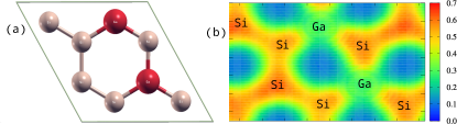
The two Ga atoms can be doped at para-ortho, para-meta, and para-para positions. These three different atomic configurations are identified as Ga2Si6-1, Ga2Si6-2, and Ga2Si6-3 for para-ortho, para-meta, and para-para positions, respectively. For instant, the atomic configuration (a) and the electronic localization function (b) of one of these structures, Ga2Si6-2 is shown in Fig. 1, where the two Ga atoms are doped at the para-meta positions.
It seems that the electron charge transfers from the Ga atoms to the Si atoms in all monolayers under investigation here, which is expected as the electronegativity of an Si atom, , is higher than that of a Ga atom, .
The energetic stability of the Ga doped silicene monolayers is gauged by a calculation of their formation energy [46]. The DFT calculations indicate that the three Ga2Si6 monolayers can be arranged from the higher to lower formation energy as follow: Ga2Si6-1 Ga2Si6-3 Ga2Si6-2. It has been shown that the lower the formation energy, the more energetically stable structure is found. As a result, the Ga2Si6-1 monolayer is the most stable structure.
The Ga atom doped in silicene will modify the electronic structure such as the lattice constant, the bond lengths, and the band gap. Tab. 1 presents the physical parameters of the four configurations, that have been considered here. We determine, that the lattice constants of GaSi7, Ga2Si6-1, Ga2Si6-2, and Ga2Si6-3 are longer than that of pure silicene. The lattice constant of pure silicene is [47]. Comparing to the lattice constant of pure silicene, the lattice constant of Ga-doped silicene is larger (see Tab. 1) indicating a supercell expansion of these Ga doped silicene monolayers. In comparison to them, the Ga2Si6-3 structure has a larger lattice constant between atoms than the others.
| Structure | a | Si-Si | Ga-Si | Ga-Ga | band gap |
|---|---|---|---|---|---|
| GaSi7 | 3.95 | 2.31 | 2.31 | - | 0.28 eV |
| Ga2Si6-1 | 4.03 | 2.28 | 2.35 | 2.43 | 0.2 meV |
| Ga2Si6-2 | 4.04 | 2.31 | 2.34 | - | 0.12 eV |
| Ga2Si6-3 | 4.05 | 2.25 | 2.38 | - | 0.6 eV |
The supercell expansion arises from the Ga-Ga interaction in the silicene structure. To determine the interaction type between the Ga-Ga atoms [48], our DFT calculations show that the interaction energy between the Ga atoms is repulsive as the interaction energy is positive. The repulsive interaction is directly proportional to the distance between Ga atoms. The repulsive interaction energy is , , and eV for Ga2Si6-1, Ga2Si6-2, and Ga2Si6-3, respectively. The modifications in the lattice constant and the bond length influence the symmetry of the structure and thus the band structures.
It has been shown that the 2D pure silicene monolayer has no band gap, similar to graphene, and the valence and conduction bands meet at the Fermi level [49, 50]. The band structure of silicene doped with Ga atoms is determined using DFT methods. The electronic band structure of the GaSi7, Ga2Si6-1, Ga2Si6-2, and Ga2Si6-3 systems is shown in Fig. 2. The doping was initially investigated at low impurity concentrations. When one Si atom is replaced with one Ga atom in a supercell, the impurity concentration rises to . Our band gap of GaSi7 is eV, as shown in Fig. 2(a), which is in good agreement with previous theoretical result of eV [51]. The Ga atom alters the band gap, causing silicene to transform from semimetal to semiconductor. Due to the presence of a finite bandgap around Fermi energy, silicene doped with Ti and V is a semiconductor, whereas Mn, Fe, and Co doped silicene is a metal because the Fermi energy penetrates the valence or the conduction bands.
It has been shown that the band gap of most monolayers is increased with the dopant concentration ratio [52, 53, 54]. This status is not true if one considers the interaction between the dopant atoms. We investigated Ga doping at impurity concentration with various Ga-Ga separations by substituting two Si atoms with two Ga atoms. There are three possible doped silicene monolayers in supercell with two Ga atoms in various positions, yielding three distinct lattice constants, and interaction energy as is seen in Tab. 1. Our findings show that the band gap is determined by the repulsive interaction between the Ga doped atoms, rather than by the amount of impurities. The band gap opens as the distance between the Ga-Ga atoms is slightly increased, while the band gap narrows as the repelling force between them increased.
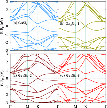
The band structure is significantly tuned, and a band gap is opened based on Ga atom configurations for the GaSi7, Ga2Si6-1, Ga2Si6-2, and Ga2Si6-3 structures.
The band gap is found to be at a maximum due to the decreased repulsive force when both of the two Ga atoms are placed at para positions in case of Ga2Si6-3, while it is reduced when they are placed at different positions of para and meta in Ga2Si6-2. However, due to the enhanced repulsive force between Ga atoms at para-ortho, the band gap of silicene is found to be very narrow, equal to meV for the Ga2Si6-1 structure.
3.2 Magnetic properties
The pure silicene was found to have no magnetism in the system, indicating that it is a nonmagnetic substance. For the varying doping concentrations of Ga atoms in silicene we compute the magnetic characteristics of the resulting material and identify possible ferromagnetic and antiferromagnetic phases.
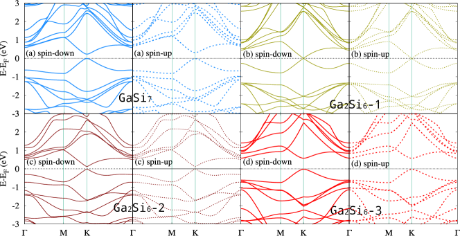
We compute the results of a spin-dependent model for the Ga-doped silicene monolayers. First, we perform both ferromagnetic (FM) and antiferromagnetic (AFM) calculations with the magnetization strength assumed to be m. The energy difference between the AFM and the FM states is . The of the Ga doped silicene is found to be zero for all structures under investigation here indicating a nonmagnetic structures. The calculations of the spin-dependent band structures can confirm the magnetic properties of the monolayers. The spin-dependent electronic band structures of GaSi7, Ga2Si6-1, Ga2Si6-2, and Ga2Si6-3 for both spin-up (solid lines) and spin-down (dotted lines) are shown in Fig. 3. The spin-up and spin-down of band structures are symmetric, and there is no spin splitting between them at the Fermi energy. It is found that the materials behave as spin unpolarized semiconductors with no spin splitting between the spin-up and spin-down channels. As a result, these materials are known as nonmagnetic semiconductors.
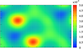
Another confirmation of the non-magnetic properties of these structures is the spin polarized density. For instance, the spin polarized density of Ga2Si6-2 is shown in Fig. 4. In both situations, FM and AFM, the distance between the atoms remains unchanged, as do the effects of both states on the lattice constant and the distance between the Ga-Ga atoms. The spin polarized density of Ga2Si6-2 is extremely small indication a non-magnetic material.
3.3 Thermal properties
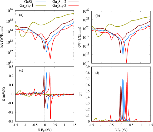
Thermal characteristics, such as the electronic thermal conductivity, the electrical conductivity, the Seebeck coefficient, and the figure of merit are examined and shown in this section. The thermal calculations are performed in the temperature range of 20–150 K. The electron contribution to transport is considerable, but the phonon contribution is negligible, and the electron and lattice temperatures are unrelated [55, 56]. Scientists have become more interested in the issue of removing heat from nanoelectronic devices and thermoelectrically turning excess heat into energy in recent years. The next generation of nanoscale electronic devices will require this thermoelectric energy conversion [57]. The figure of merit, which is connected to the Seebeck coefficient, the electrical conductivity, the temperature, and the electronic thermal conductivity, determines the efficiency of heat conversion. It has been proven that a material with a high figure of merit should have a high electrical conductivity and Seebeck coefficient, and low thermal conductivity with a specificity temperature. A thermoelectric device’s or material’s efficiency is evaluated by its thermoelectric figure of merit, which is defined as [58], where is the Seeback coefficient, is the electrical conductance, the temperature and the electronic thermal conductance. A monolayer silicene’s thermoelectric performance is low due to closeness of its band gaps. Pure silicene has a low and a high , resulting in a low [35]. Figure 5 indicates the relationship between (a), (b), (c), and (d) with energy. Lowering the , which enhances the structure and increases the , is achieved by doping silicene. The decrease in the value of is found to be significantly higher than the change in . Doping Ga in silicene opens the band gap, which is dependent of the distance between dopant atoms rather than the increase in concentration. The and in GaSi7, Ga2Si6-1, Ga2Si6-2, and Ga2Si6-3 structures are estimated to rise. The Ga2Si6-1 has a low band gap, but Ga2Si6-3 has the largest band gap, resulting in the highest and . The other structures GaSi7, Ga2Si6-1 fall between them. As a result, the Ga2Si6-3 should perform better in terms of thermoelectricity.
3.4 Optical properties
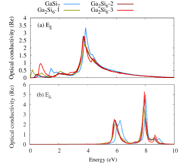
In this part, we calculate the optical properties, such as the imaginary part of the dielectric function, , the excitation spectra, , and the optical conductivity for 2D Ga-doped silicene in parallel (E∥) and perpendicular (E⟂) polarized electric fields. The electronic band structure has a direct impact on the optical properties. As a result, changing the band gap of a material has an effect on its optical characteristics. The dielectric function is widely used to evaluate the optical properties, and it can also be used to describe other qualities. The material’s ability to absorb energy is proportional to the imaginary component of the dielectric function.
There are two primary peaks in , and for for silicene with no doping [59]. In the M-K direction, the transition occurs at eV, whereas the transition occurs at eV in both the M-K and -K directions. For the case of E⟂, interband transitions have been reported, and the transitions occur at energies below 10 eV [59].
We show the (a,b) and excitation spectra (c,d) for light polarized parallel and perpendicular to the plane of the GaSi7, Ga2Si6-1, Ga2Si6-2, and Ga2Si6-3 in Fig. 6. The dielectric function and the excitation spectra are affected by the repulsive interaction of the Ga-Ga atoms as the band structure and the band gap are tuned due to the Ga atoms. Both peaks occur with a little shift to lower energy in both directions, and the high peak is created at low energy for the imaginary part of the dielectric function. Ga2Si6-3 has the highest pick among the structures because of the largest band gap arising from the minimized repulsive force between Ga atoms.

The last part of this study is the influence of doping on the optical conductivity (real part) of GaSi7, Ga2Si6-1, Ga2Si6-2, and Ga2Si6-3 structures in parallel and perpendicular electric fields as shown in Fig. 7. For these structures, the optical conductivity in E∥ is almost zero up to eV, meV, eV, and eV, indicating the band gap of these monolayers, which have semiconductors properties. The Ga2Si6-3 has the highest peak value in terms of low energy among them due to its repelling action.
4 Conclusion
The effects of the atomic configuration, the interatomic distance, and the atomic interaction of the dopant atoms with silicene are given special consideration in this study. Despite its favorable properties, silicene, like graphene, has a zero band gap, which restricts its application in nanodevices. We show that a Ga doped silicene monolayer opens a band gap. The configuration and the dopant concentration ratio control the band gap according to the first-principles calculations. The effects of doping has been examined by changing the dopant concentrations from to , as well as examining alternative atomic positions for the same replacement doping concentration. The band gap in a 2D silicene doped with Ga is seen to be significantly dependent on the location of the Ga atoms and the Ga-Ga interactions. The band gap is determined by the distance between the dopant atoms and the Coulomb repulsive force, rather than the doping concentration. As a result, the band gap in a monolayer of silicene can be widened, resulting in enhanced thermoelectric and optical properties. Furthermore, these structures behave as nonmagnetic semiconductors because they are spin unpolarized and have no spin splitting between spin-up and spin-down levels in the band structure. Finally, our calculations revealed that Ga doped silicene monolayers will be beneficial for thermoelectric and optoelectronic devices.
References
-
[1]
N. Baig, I. Kammakakam, W. Falath,
Nanomaterials: a review of
synthesis methods, properties, recent progress, and challenges, Mater.
Adv. 2 (2021) 1821–1871.
doi:10.1039/D0MA00807A.
URL http://dx.doi.org/10.1039/D0MA00807A -
[2]
J. H. Kim, J. H. Jeong, N. Kim, R. Joshi, G.-H. Lee,
Mechanical properties of
two-dimensional materials and their applications, Journal of Physics D:
Applied Physics 52 (8) (2018) 083001.
doi:10.1088/1361-6463/aaf465.
URL https://doi.org/10.1088/1361-6463/aaf465 -
[3]
N. R. Abdullah,
Outstanding
performance of si-bilayer graphene using first-principle computation:
Significant effects of si atoms configuration, Physica B: Condensed Matter
620 (2021) 413273.
doi:https://doi.org/10.1016/j.physb.2021.413273.
URL https://www.sciencedirect.com/science/article/pii/S0921452621004464 -
[4]
S. Z. Butler, S. M. Hollen, L. Cao, Y. Cui, J. A. Gupta, H. R. Gutiérrez,
T. F. Heinz, S. S. Hong, J. Huang, A. F. Ismach, E. Johnston-Halperin,
M. Kuno, V. V. Plashnitsa, R. D. Robinson, R. S. Ruoff, S. Salahuddin,
J. Shan, L. Shi, M. G. Spencer, M. Terrones, W. Windl, J. E. Goldberger,
Progress, challenges, and
opportunities in two-dimensional materials beyond graphene, ACS Nano 7 (4)
(2013) 2898–2926, pMID: 23464873.
arXiv:https://doi.org/10.1021/nn400280c, doi:10.1021/nn400280c.
URL https://doi.org/10.1021/nn400280c -
[5]
X. Yu, H. Cheng, M. Zhang, Y. Zhao, L. Qu, G. Shi,
Graphene-based smart
materials, Nature Reviews Materials 2 (9) (2017) 17046.
doi:10.1038/natrevmats.2017.46.
URL https://doi.org/10.1038/natrevmats.2017.46 -
[6]
A. Borenstein, O. Hanna, R. Attias, S. Luski, T. Brousse, D. Aurbach,
Carbon-based composite materials
for supercapacitor electrodes: a review, J. Mater. Chem. A 5 (2017)
12653–12672.
doi:10.1039/C7TA00863E.
URL http://dx.doi.org/10.1039/C7TA00863E -
[7]
H. Oughaddou, H. Enriquez, M. R. Tchalala, H. Yildirim, A. J. Mayne,
A. Bendounan, G. Dujardin, M. Ait Ali, A. Kara,
Silicene,
a promising new 2d material, Progress in Surface Science 90 (1) (2015)
46–83, special Issue on Silicene.
doi:https://doi.org/10.1016/j.progsurf.2014.12.003.
URL https://www.sciencedirect.com/science/article/pii/S0079681614000331 -
[8]
A. M. Tokmachev, D. V. Averyanov, O. E. Parfenov, A. N. Taldenkov, I. A.
Karateev, I. S. Sokolov, O. A. Kondratev, V. G. Storchak,
Emerging two-dimensional
ferromagnetism in silicene materials, Nature Communications 9 (1) (2018)
1672.
doi:10.1038/s41467-018-04012-2.
URL https://doi.org/10.1038/s41467-018-04012-2 -
[9]
G. G. Guzmán-Verri, L. C. Lew Yan Voon,
Electronic
structure of silicon-based nanostructures, Phys. Rev. B 76 (2007) 075131.
doi:10.1103/PhysRevB.76.075131.
URL https://link.aps.org/doi/10.1103/PhysRevB.76.075131 -
[10]
L. C. Lew Yan Voon, J. Zhu, U. Schwingenschlögl,
Silicene: Recent theoretical
advances, Applied Physics Reviews 3 (4) (2016) 040802.
arXiv:https://doi.org/10.1063/1.4944631, doi:10.1063/1.4944631.
URL https://doi.org/10.1063/1.4944631 -
[11]
P. Vogt, P. De Padova, C. Quaresima, J. Avila, E. Frantzeskakis, M. C. Asensio,
A. Resta, B. Ealet, G. Le Lay,
Silicene:
Compelling experimental evidence for graphenelike two-dimensional silicon,
Phys. Rev. Lett. 108 (2012) 155501.
doi:10.1103/PhysRevLett.108.155501.
URL https://link.aps.org/doi/10.1103/PhysRevLett.108.155501 -
[12]
C.-L. Lin, R. Arafune, K. Kawahara, N. Tsukahara, E. Minamitani, Y. Kim,
N. Takagi, M. Kawai, Structure
of silicene grown on ag(111), Applied Physics Express 5 (4) (2012) 045802.
doi:10.1143/apex.5.045802.
URL https://doi.org/10.1143/apex.5.045802 -
[13]
H. Jamgotchian, Y. Colignon, N. Hamzaoui, B. Ealet, J. Y. Hoarau, B. Aufray,
J. P. Bibérian,
Growth of silicene
layers on ag(111): unexpected effect of the substrate temperature, Journal
of Physics: Condensed Matter 24 (17) (2012) 172001.
doi:10.1088/0953-8984/24/17/172001.
URL https://doi.org/10.1088/0953-8984/24/17/172001 -
[14]
B. Feng, Z. Ding, S. Meng, Y. Yao, X. He, P. Cheng, L. Chen, K. Wu,
Evidence of silicene in honeycomb
structures of silicon on ag(111), Nano Letters 12 (7) (2012) 3507–3511,
pMID: 22658061.
arXiv:https://doi.org/10.1021/nl301047g, doi:10.1021/nl301047g.
URL https://doi.org/10.1021/nl301047g -
[15]
R. Arafune, C.-L. Lin, K. Kawahara, N. Tsukahara, E. Minamitani, Y. Kim,
N. Takagi, M. Kawai,
Structural
transition of silicene on ag(111), Surface Science 608 (2013) 297–300.
doi:https://doi.org/10.1016/j.susc.2012.10.022.
URL https://www.sciencedirect.com/science/article/pii/S0039602812003925 -
[16]
A. Fleurence, R. Friedlein, T. Ozaki, H. Kawai, Y. Wang, Y. Yamada-Takamura,
Experimental
evidence for epitaxial silicene on diboride thin films, Phys. Rev. Lett. 108
(2012) 245501.
doi:10.1103/PhysRevLett.108.245501.
URL https://link.aps.org/doi/10.1103/PhysRevLett.108.245501 -
[17]
L. Meng, Y. Wang, L. Zhang, S. Du, R. Wu, L. Li, Y. Zhang, G. Li, H. Zhou,
W. A. Hofer, H.-J. Gao, Buckled
silicene formation on ir(111), Nano Letters 13 (2) (2013) 685–690, pMID:
23330602.
arXiv:https://doi.org/10.1021/nl304347w, doi:10.1021/nl304347w.
URL https://doi.org/10.1021/nl304347w -
[18]
T. Aizawa, S. Suehara, S. Otani,
Phonon dispersion of
silicene on ZrB2(0 0 0 1), Journal of Physics: Condensed Matter 27 (30)
(2015) 305002.
doi:10.1088/0953-8984/27/30/305002.
URL https://doi.org/10.1088/0953-8984/27/30/305002 -
[19]
J. Zhu, U. Schwingenschlögl,
Silicene on MoS2: role
of the van der waals interaction, 2D Materials 2 (4) (2015) 045004.
doi:10.1088/2053-1583/2/4/045004.
URL https://doi.org/10.1088/2053-1583/2/4/045004 -
[20]
D. Chiappe, E. Scalise, E. Cinquanta, C. Grazianetti, B. van den Broek,
M. Fanciulli, M. Houssa, A. Molle,
Two-dimensional
si nanosheets with local hexagonal structure on a mos2 surface, Advanced
Materials 26 (13) (2014) 2096–2101.
arXiv:https://onlinelibrary.wiley.com/doi/pdf/10.1002/adma.201304783,
doi:https://doi.org/10.1002/adma.201304783.
URL https://onlinelibrary.wiley.com/doi/abs/10.1002/adma.201304783 -
[21]
H. Liu, J. Gao, J. Zhao, Silicene on
substrates: A way to preserve or tune its electronic properties, The Journal
of Physical Chemistry C 117 (20) (2013) 10353–10359.
arXiv:https://doi.org/10.1021/jp311836m, doi:10.1021/jp311836m.
URL https://doi.org/10.1021/jp311836m -
[22]
L. Tao, E. Cinquanta, D. Chiappe, C. Grazianetti, M. Fanciulli, M. Dubey,
A. Molle, D. Akinwande,
Silicene field-effect
transistors operating at room temperature, Nature Nanotechnology 10 (3)
(2015) 227–231.
doi:10.1038/nnano.2014.325.
URL https://doi.org/10.1038/nnano.2014.325 -
[23]
M. Takahashi, Flat building
blocks for flat silicene, Scientific Reports 7 (1) (2017) 10855.
doi:10.1038/s41598-017-11360-4.
URL https://doi.org/10.1038/s41598-017-11360-4 -
[24]
A. Molle, C. Grazianetti, L. Tao, D. Taneja, M. H. Alam, D. Akinwande,
Silicene, silicene
derivatives, and their device applications, Chem. Soc. Rev. 47 (2018)
6370–6387.
doi:10.1039/C8CS00338F.
URL http://dx.doi.org/10.1039/C8CS00338F -
[25]
D. Jose, A. Datta, Structures and
chemical properties of silicene: Unlike graphene, Accounts of Chemical
Research 47 (2) (2014) 593–602, pMID: 24215179.
arXiv:https://doi.org/10.1021/ar400180e, doi:10.1021/ar400180e.
URL https://doi.org/10.1021/ar400180e -
[26]
S.-Y. Lin, S.-L. Chang, N. T. Thuy Tran, P.-H. Yang, M.-F. Lin,
H–si bonding-induced unusual
electronic properties of silicene: a method to identify hydrogen
concentration, Phys. Chem. Chem. Phys. 17 (2015) 26443–26450.
doi:10.1039/C5CP04841A.
URL http://dx.doi.org/10.1039/C5CP04841A -
[27]
D. K. Nguyen, N. T. T. Tran, Y.-H. Chiu, M.-F. Lin,
Concentration-diversified
magnetic and electronic properties of halogen-adsorbed silicene, Scientific
Reports 9 (1) (2019) 13746.
doi:10.1038/s41598-019-50233-w.
URL https://doi.org/10.1038/s41598-019-50233-w -
[28]
Y. Du, J. Zhuang, H. Liu, X. Xu, S. Eilers, K. Wu, P. Cheng, J. Zhao, X. Pi,
K. W. See, G. Peleckis, X. Wang, S. X. Dou,
Tuning the band gap in silicene by
oxidation, ACS Nano 8 (10) (2014) 10019–10025, pMID: 25248135.
arXiv:https://doi.org/10.1021/nn504451t, doi:10.1021/nn504451t.
URL https://doi.org/10.1021/nn504451t -
[29]
X.-L. Zhang, L.-F. Liu, W.-M. Liu,
Quantum anomalous hall effect and
tunable topological states in 3d transition metals doped silicene,
Scientific Reports 3 (1) (2013) 2908.
doi:10.1038/srep02908.
URL https://doi.org/10.1038/srep02908 -
[30]
A. Manjanath, V. Kumar, A. K. Singh,
Mechanical and electronic
properties of pristine and ni-doped si, ge, and sn sheets, Phys. Chem.
Chem. Phys. 16 (2014) 1667–1671.
doi:10.1039/C3CP54655A.
URL http://dx.doi.org/10.1039/C3CP54655A -
[31]
R. Das, S. Chowdhury, A. Majumdar, D. Jana,
Optical properties of p and al
doped silicene: a first principles study, RSC Adv. 5 (2015) 41–50.
doi:10.1039/C4RA07976K.
URL http://dx.doi.org/10.1039/C4RA07976K -
[32]
H. Hernández Cocoletzi, J. Castellanos Águila,
Dft
studies on the al, b, and p doping of silicene, Superlattices and
Microstructures 114 (2018) 242–250.
doi:https://doi.org/10.1016/j.spmi.2017.12.040.
URL https://www.sciencedirect.com/science/article/pii/S0749603617325193 -
[33]
R. Pablo-Pedro, M. A. Magaña-Fuentes, M. Videa, J. Kong, M. Li, J. L.
Mendoza-Cortes, T. Van Voorhis,
Understanding disorder in
2d materials: The case of carbon doping of silicene, Nano Letters 20 (9)
(2020) 6336–6343, pMID: 32787169.
arXiv:https://doi.org/10.1021/acs.nanolett.0c01775, doi:10.1021/acs.nanolett.0c01775.
URL https://doi.org/10.1021/acs.nanolett.0c01775 -
[34]
N. R. Abdullah, M. T. Kareem, H. O. Rashid, A. Manolescu, V. Gudmundsson,
Spin-polarised
dft modeling of electronic, magnetic, thermal and optical properties of
silicene doped with transition metals, Physica E: Low-dimensional Systems
and Nanostructures 129 (2021) 114644.
doi:https://doi.org/10.1016/j.physe.2021.114644.
URL https://www.sciencedirect.com/science/article/pii/S1386947721000266 -
[35]
W.-Z. Li, M.-Y. Liu, L. Gong, Q.-Y. Chen, C. Cao, Y. He,
Emerging
various electronic and magnetic properties of silicene by light rare-earth
metal substituted doping, Superlattices and Microstructures 148 (2020)
106712.
doi:https://doi.org/10.1016/j.spmi.2020.106712.
URL https://www.sciencedirect.com/science/article/pii/S0749603620312611 -
[36]
N. T. T. Tran, G. Gumbs, D. K. Nguyen, M.-F. Lin,
Fundamental properties of
metal-adsorbed silicene: A dft study, ACS Omega 5 (23) (2020) 13760–13769.
arXiv:https://doi.org/10.1021/acsomega.0c00905, doi:10.1021/acsomega.0c00905.
URL https://doi.org/10.1021/acsomega.0c00905 -
[37]
P. Giannozzi, S. Baroni, N. Bonini, M. Calandra, R. Car, C. Cavazzoni,
D. Ceresoli, G. L. Chiarotti, M. Cococcioni, I. Dabo, A. D. Corso,
S. de Gironcoli, S. Fabris, G. Fratesi, R. Gebauer, U. Gerstmann,
C. Gougoussis, A. Kokalj, M. Lazzeri, L. Martin-Samos, N. Marzari, F. Mauri,
R. Mazzarello, S. Paolini, A. Pasquarello, L. Paulatto, C. Sbraccia,
S. Scandolo, G. Sclauzero, A. P. Seitsonen, A. Smogunov, P. Umari, R. M.
Wentzcovitch,
QUANTUM
ESPRESSO: a modular and open-source software project for quantum
simulations of materials, Journal of Physics: Condensed Matter 21 (39)
(2009) 395502.
doi:10.1088/0953-8984/21/39/395502.
URL https://doi.org/10.1088%2F0953-8984%2F21%2F39%2F395502 - [38] P. Giannozzi, O. Andreussi, T. Brumme, O. Bunau, M. B. Nardelli, M. Calandra, R. Car, C. Cavazzoni, D. Ceresoli, M. Cococcioni, et al., Advanced capabilities for materials modelling with quantum espresso, Journal of Physics: Condensed Matter 29 (46) (2017) 465901.
-
[39]
A. Kokalj,
Xcrysden—a
new program for displaying crystalline structures and electron densities,
Journal of Molecular Graphics and Modelling 17 (3) (1999) 176–179.
doi:10.1016/S1093-3263(99)00028-5.
URL http://www.sciencedirect.com/science/article/pii/S1093326399000285 - [40] K. Momma, F. Izumi, Vesta 3 for three-dimensional visualization of crystal, volumetric and morphology data, Journal of applied crystallography 44 (6) (2011) 1272–1276.
-
[41]
N. R. Abdullah, H. O. Rashid, V. Gudmundsson,
Study
of bc14n-bilayer graphene: Effects of atomic spacing and interatomic
interaction between b and n atoms, Superlattices and Microstructures 156
(2021) 106981.
doi:https://doi.org/10.1016/j.spmi.2021.106981.
URL https://www.sciencedirect.com/science/article/pii/S0749603621001798 -
[42]
G. K. H. Madsen, D. J. Singh,
Boltztrap.
a code for calculating band-structure dependent quantities, Computer Physics
Communications 175 (1) (2006) 67–71.
URL http://www.sciencedirect.com/science/article/pii/S0010465506001305 -
[43]
N. R. Abdullah, B. J. Abdullah, C.-S. Tang, V. Gudmundsson,
Properties
of bc6n monolayer derived by first-principle computation: Influences of
interactions between dopant atoms on thermoelectric and optical properties,
Materials Science in Semiconductor Processing 135 (2021) 106073.
doi:https://doi.org/10.1016/j.mssp.2021.106073.
URL https://www.sciencedirect.com/science/article/pii/S1369800121004182 -
[44]
H. O. Rashid, N. R. Abdullah, V. Gudmundsson,
Silicon
on a graphene nanosheet with triangle- and dot-shape: Electronic structure,
specific heat, and thermal conductivity from first-principle calculations,
Results in Physics 15 (2019) 102625.
doi:10.1016/j.rinp.2019.102625.
URL http://www.sciencedirect.com/science/article/pii/S2211379719317140 -
[45]
N. R. Abdullah, H. O. Rashid, C.-S. Tang, A. Manolescu, V. Gudmundsson,
Role
of interlayer spacing on electronic, thermal and optical properties of
bn-codoped bilayer graphene: Influence of the interlayer and the induced
dipole-dipole interactions, Journal of Physics and Chemistry of Solids 155
(2021) 110095.
doi:https://doi.org/10.1016/j.jpcs.2021.110095.
URL https://www.sciencedirect.com/science/article/pii/S002236972100161X -
[46]
N. R. Abdullah, H. O. Rashid, C.-S. Tang, A. Manolescu, V. Gudmundsson,
Properties
of bsi6n monolayers derived by first-principle computation, Physica E:
Low-dimensional Systems and Nanostructures (2020) 114556doi:https://doi.org/10.1016/j.physe.2020.114556.
URL http://www.sciencedirect.com/science/article/pii/S1386947720316246 - [47] N. R. Abdullah, H. O. Rashid, A. Manolescu, V. Gudmundsson, Interaction effects in a two-dimensional alsi p nanosheet: A first-principles study on the electronic, mechanical, thermal, and optical properties, arXiv preprint arXiv:2108.00387 (2021).
-
[48]
N. R. Abdullah, H. O. Rashid, M. T. Kareem, C.-S. Tang, A. Manolescu,
V. Gudmundsson,
Effects
of bonded and non-bonded b/n codoping of graphene on its stability,
interaction energy, electronic structure, and power factor, Physics Letters
A 384 (12) (2020) 126350.
doi:10.1016/j.physleta.2020.126350.
URL http://www.sciencedirect.com/science/article/pii/S0375960120301602 -
[49]
K. Takeda, K. Shiraishi,
Theoretical
possibility of stage corrugation in si and ge analogs of graphite, Phys.
Rev. B 50 (1994) 14916–14922.
doi:10.1103/PhysRevB.50.14916.
URL https://link.aps.org/doi/10.1103/PhysRevB.50.14916 -
[50]
N. R. Abdullah, H. O. Rashid, C.-S. Tang, A. Manolescu, V. Gudmundsson,
Modeling
electronic, mechanical, optical and thermal properties of graphene-like bc6n
materials: Role of prominent bn-bonds, Physics Letters A 384 (32) (2020)
126807.
doi:https://doi.org/10.1016/j.physleta.2020.126807.
URL http://www.sciencedirect.com/science/article/pii/S0375960120306745 -
[51]
Pamungkas, Mauludi Ariesto, Maftuhin, Wafa,
Electronic structures of
silicene doped with galium: First principle study, MATEC Web of Conferences
30 (2015) 03003.
doi:10.1051/matecconf/20153003003.
URL https://doi.org/10.1051/matecconf/20153003003 -
[52]
Z. Ni, H. Zhong, X. Jiang, R. Quhe, G. Luo, Y. Wang, M. Ye, J. Yang, J. Shi,
J. Lu, Tunable band gap and
doping type in silicene by surface adsorption: towards tunneling
transistors, Nanoscale 6 (2014) 7609–7618.
doi:10.1039/C4NR00028E.
URL http://dx.doi.org/10.1039/C4NR00028E -
[53]
A. Hussain, S. Ullah, M. A. Farhan,
Fine tuning the band-gap of
graphene by atomic and molecular doping: a density functional theory study,
RSC Adv. 6 (2016) 55990–56003.
doi:10.1039/C6RA04782C.
URL http://dx.doi.org/10.1039/C6RA04782C -
[54]
N. R. Abdullah, H. O. Rashid, A. Manolescu, V. Gudmundsson,
Interlayer
interaction controlling the properties of ab- and aa-stacked bilayer
graphene-like bc14n and si2c14, Surfaces and Interfaces 21 (2020) 100740.
doi:https://doi.org/10.1016/j.surfin.2020.100740.
URL http://www.sciencedirect.com/science/article/pii/S246802302030732X -
[55]
D. L. Nika, A. A. Balandin,
Two-dimensional phonon
transport in graphene, Journal of Physics: Condensed Matter 24 (23) (2012)
233203.
doi:10.1088/0953-8984/24/23/233203.
URL https://doi.org/10.1088/0953-8984/24/23/233203 -
[56]
Y. Cheng, X. Wu, Z. Zhang, Y. Sun, Y. Zhao, Y. Zhang, G. Zhang,
Thermo-mechanical correlation in
two-dimensional materials, Nanoscale 13 (2021) 1425–1442.
doi:10.1039/D0NR06824A.
URL http://dx.doi.org/10.1039/D0NR06824A -
[57]
H. Sadeghi, S. Sangtarash, C. J. Lambert,
Enhanced thermoelectric efficiency
of porous silicene nanoribbons, Scientific Reports 5 (1) (2015) 9514.
doi:10.1038/srep09514.
URL https://doi.org/10.1038/srep09514 -
[58]
J. Wang, X. Mu, M. Sun, The
thermal, electrical and thermoelectric properties of graphene nanomaterials,
Nanomaterials 9 (2) (2019).
doi:10.3390/nano9020218.
URL https://www.mdpi.com/2079-4991/9/2/218 -
[59]
R. John, B. Merlin,
Optical
properties of graphene, silicene, germanene, and stanene from ir to far uv
– a first principles study, Journal of Physics and Chemistry of Solids 110
(2017) 307 – 315.
doi:https://doi.org/10.1016/j.jpcs.2017.06.026.
URL http://www.sciencedirect.com/science/article/pii/S0022369717300367