First-principles ionized-impurity scattering and charge transport in doped materials
Abstract
Scattering of carriers with ionized impurities governs charge transport in doped semiconductors. However, electron interactions with ionized impurities cannot be fully described with quantitative first-principles calculations, so their understanding relies primarily on simplified models. Here we show an ab initio approach to compute the interactions between electrons and ionized impurities or other charged defects. It includes the short- and long-range electron-defect (-d) interactions on equal footing, and allows for efficient interpolation of the -d matrix elements. We combine the -d and electron-phonon interactions in the Boltzmann transport equation to compute the carrier mobilities in doped silicon over a wide range of temperature and doping concentrations, spanning seamlessly the defect- and phonon-limited transport regimes. The individual contributions of the defect- and phonon-scattering mechanisms to the carrier relaxation times and mean-free paths are analyzed. Our method provides a powerful tool to study electronic interactions in doped materials. It broadens the scope of first-principles transport calculations, enabling studies of a wide range of doped semiconductors and oxides with application to electronics, energy and quantum technologies.
Scattering of carriers with charged defects is treated primarily using heuristic models. An important example are calculations of ionized-impurity scattering in doped semiconductors and the resulting defect-limited transport properties.
Widely adopted models neglect the detailed atomic structure of the defects, employ approximate defect-scattering potentials, and rely on simplified electronic band structures usually, a single isotropic band parametrized by the effective mass [1, 2, 3].
First-principles calculations of electron-defect (-d) interactions for ionized impurities and other charged defects remain an open challenge. Their development would enable quantitative studies of transport in doped materials with complex atomic and electronic structures, providing microscopic insight into the effects of dopants in a wide range of technological materials and devices.
Recent work has highlighted the computational cost and difficult workflows for obtaining -d interactions in the framework on density functional theory (DFT) [4, 5, 6], particularly when using fine Brillouin zone (BZ) grids required for transport calculations [7, 8, 5, 6]. Various approximations have been employed to obviate these bottlenecks, such as treating the charged-defect perturbation as a Yukawa potential [9, 10] or the Bloch electronic states as plane waves [11].
Recent work by us [5, 6] and Kaasbjerg et al. [12] has developed a fully ab initio framework, based on DFT, to compute e-d interactions without simplifying approximations, so far focusing on charge-neutral defects [12, 5, 6].
Despite these advances, an efficient ab initio method to compute e-d interactions for charged defects and study their impact on charge transport is still missing. Ideally, such an approach would capture the atomic details of the defect perturbation potential, use electronic Bloch wave functions, and employ the full band structure of the material.
Here, we show a first-principles method to efficiently compute the e-d interactions for ionized impurities and other charged defects. Our approach is based on plane-wave DFT calculations and satisfies all the ideal characteristics listed above.
To obtain the -d matrix elements, we develop approaches for supercell potential-alignment and removal of spurious image contributions. Both the short- and long-range perturbations induced by the charged defects are included, without using any empirical or tuning parameters.
We combine the e-d and electron-phonon (e-ph) interactions in the Boltzmann transport equation (BTE) to compute the carrier mobility in a doped material with an accurate account of ionized-impurity scattering.
We apply our method to silicon doped with phosphorous (P) or boron (B); we compute and analyze state-dependent relaxation times (RTs) for ionized-impurity scattering, and predict the doping and temperature dependence of the electron and hole mobilities in quantitative agreement with experiment.
Our treatment of electron-charged defect interactions complements recent efforts to develop quantitative tools to study charge transport in real materials [8, 13, 14, 6, 15, 16, 17].
The -d matrix element coupling a Bloch state , with band index and crystal momentum , to another state due to the perturbation potential from a charged defect, , is defined as
| (1) |
where the Bloch states are for the pristine system without any defect [5].
The -d defect perturbation potential is obtained from DFT calculations as the difference between the Kohn-Sham (KS) potential of the pristine system and that of the same system containing a defect [5].
We use two supercells with the same size to simulate the pristine and defect-containing systems.
For charged defects, the difference between the KS Hamiltonians of these two supercells, , is not equal to the -d perturbation, and requires a correction that is not needed for charge-neutral defects [5].
To treat charged defects in plane-wave DFT, the widely-used Jellium model [18] removes the divergence due to the charge introduced in the supercell by setting to zero the component of the Hartree potential ( are reciprocal lattice vectors of the supercell).
Although the divergence has been removed, the supercell is, in a sense, still charged since a uniform electron density is added to the system, the long-range tail of the Coulomb potential generated by the charged defect is still present [19].
As a result, the charged-defect perturbation potential does not decay to zero inside the supercell, and therefore is contaminated by the periodic images of the supercell.
To remove these spurious contributions, we introduce a supercell-periodic screened-Coulomb potential, , generated from a point charge (where is the electron charge) in the supercell, which simulates the charge state of the defect:
| (2) |
where is the volume of the supercell. The Fourier coefficient at wave vector of this screened-Coulomb potential is defined as
| (3) |
where is the vacuum permittivity and is the dielectric function due to the screening from the valence electrons, described here using an isotropic homogeneous electron model. The spurious image-cell contributions are then removed by subtracting from the KS perturbation potential. An additional correction is needed to account for DFT potential-alignment errors due to the different potential references used in the pristine and defect-containing supercell calculations [5]. With these corrections, we compute the neutral part of the -d perturbation potential as
| (4) |
where the term enforces the potential alignment.
Finally, we obtain the charged-defect perturbation potential, , by adding the screened-Coulomb potential due to an isolated point charge, ; the latter is screened by both the valence electrons and by any extrinsic free carriers (with concentration ) resulting from ionized impurities:
| (5) |
with the Fourier coefficient of the screened-Coulomb potential of the isolated defect computed as [20]
| (6) |
Above, is the dielectric constant, and the inverse screening length due to the free carriers is [21]
| (7) |
where is the density of states (DOS) at electron energy , is the conduction band minimum, and is the Fermi-Dirac distribution.
This expression is for electrons, but a similar one holds for hole carriers [21].
Substituting Eq. (5) into Eq. (1) splits the -d matrix element for a charged defect into two parts,
| (8) |
The first term, , is a short-ranged charge-neutral contribution, while the second term, , accounts for the long-range screened Coulomb interaction generated by the charged defect (with the spurious image contributions properly removed).
In practice, the -d matrix elements are computed using the approach developed in Ref [5], using wave functions from a primitive unit cell (as opposed to the large supercell) to greatly reduce the computational cost.
The Wannier function (WF) interpolation scheme we recently developed for charge-neutral defects [6] is then employed to interpolate the neutral part of the matrix elements, , on ultra-fine BZ grids.
For the long-range part, , we develop a different interpolation approach inspired by recent work on -ph interactions in polar materials (for details, see the Supplemental Material [22]).
With the ab initio ionized-impurity scattering in hand, we combine -ph and elastic -d interactions in the BTE framework to compute the carrier mobility as a function of temperature and doping concentration [23, 7].
The conductivity tensor is computed using [24, 25, 14]
| (9) |
where and are Cartesian directions; the mobility is obtained using , where is the carrier concentration. The transport distribution function is defined as [14]
| (10) |
where is the spin degeneracy and is the number of -points in the BZ; and are electron band energies and velocities, respectively. The vector is proportional to the steady-state occupation change of each electronic state [14], and is obtained by solving the linearized BTE for a weak electric field. Extending the approach developed in Perturbo [14] to include both -d and -ph interactions, the BTE becomes:
| (11) |
where and are the numbers of -points and -points in the BZ, respectively. The -ph scattering rate for each electronic state, , is computed using [14]
| (12) |
where is the scattering rate from state to due to the emission or absorption of a phonon with mode index and crystal momentum [14]. The -d scattering rate is defined analogously as
| (13) |
where is the elastic -d scattering rate between two electronic states due to a charged defect [5]:
| (14) |
In this expression, is the number of atoms in the primitive cell and the scattering rate is proportional to the impurity concentration , defined as in Ref. [5] as the dimensionless ratio of the number of impurities to the total number of atoms in the crystal.
The -ph and -d relaxation times (RTs) for each electronic state are obtained as the inverse of the respective scattering rates,
and .
The occupation change vector in Eq. (11) can be obtained with an iterative approach (ITA) to solve the BTE [26, 14], or alternatively by using the relaxation-time approximation (RTA), where backscattering is neglected by setting to zero the two summations in the right-hand side of Eq. (11).
For elastic -d interactions, a widely used approach to approximately account for backscattering is to use the RTA with the -d scattering rates multiplied by a cosine factor [25].
These so-called transport -d scattering rates are defined as [25]:
| (15) |
where is the angle between the band velocities and . Using these transport -d scattering rates in the left-hand side of Eq. (11), while leaving out the backscattering terms in the right-hand side, leads to the transport relaxation-time approximation (tr-RTA).
In this work, we first obtain the occupation changes by solving the BTE in one of the three flavors described above (ITA, RTA or tr-RTA). We then compute the conductivity using Eq. (9), and from it obtain the carrier mobility .
Our approach allows us to include scattering from both the -d interactions due to charged defects (here, ionized impurities) and the -ph interactions.
We can also obtain the mobility limited by only one of the -ph or -d interactions, by leaving out, respectively, the defect or phonon scattering terms in the BTE.
The formalism discussed above has been implemented in our open-source code, Perturbo [14].
We apply our approach to Si doped with phosphorous (P) or boron (B), respectively to study electron or hole carriers;
for now, we assume that the dopants are fully ionized.
We carry out plane-wave DFT calculations [27] with norm-conserving pseudopotentials [28] using the Quantum Espresso code [29] (numerical details are provided below [30]).
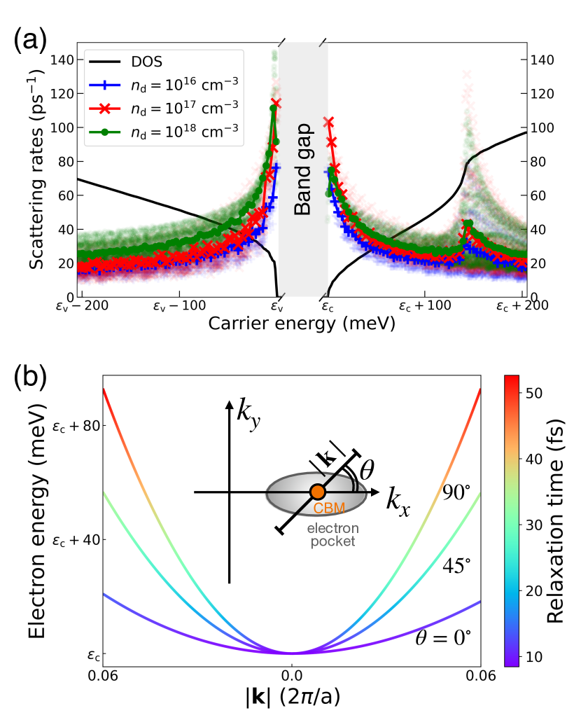
Figure 1(a) shows our computed -d scattering rates for electron and hole majority carriers in doped Si at K, for doping concentrations of cm-3.
The -d scattering rates decrease for increasing carrier energy, referenced to the valence band maximum (VBM) for holes and conduction band minimum (CBM) for electrons. This trend is opposite to neutral-defect scattering [5], where the scattering rates increase with carrier energy due to the greater electronic DOS, which measures the number of accessible final states for elastic -d scattering.
Our results show that this phase-space argument does not hold for charged defects, where the momentum dependence of the -d matrix elements plays a dominant role since the matrix elements increase rapidly for decreasing transferred momenta ,
the -d scattering rates are greater near the valence and conduction band edges, despite the small DOS values.
For the same reason, we find a peak in the electron scattering rates meV above the CBM in correspondence with a band crossing. Note also how increasing doping levels lead to stronger -d scattering (and thus greater scattering rates), a relevant sanity check for our calculations.
Our approach can capture the momentum dependence of the scattering rates. At each given carrier energy, the scattering rates exhibit a range of values due to the anisotropic character of the band structure and scattering processes.
To highlight this point, Fig. 1(b) shows the state-dependent RTs for electronic states in the lowest conduction band along three different paths passing through the CBM.
These paths, chosen to lie in the - plane, are specified by an angle measured from the axis (i.e., the X direction in the BZ), so that is the longitudinal, and the transverse valley direction [3].
For a fixed carrier energy here, meV above the CBM the RTs for , , and are 10, 20, and 30 fs respectively, thus demonstrating that electronic states with the same energy can have a broad distribution of RTs.
Our ability to treat -d scattering for anisotropic, multi-valley band structures is key for studies of defect-limited transport in complex materials.
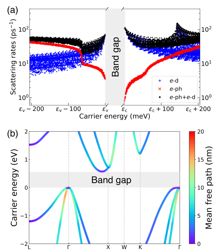
Next, we examine the individual and combined effects of the -ph and -d interactions in a doped material [see Fig. 2(a)].
Different from the ionized-impurity case, the -ph scattering rates increase with carrier energy due to the dominant role of the scattering phase-space.
As a consequence, -d scattering from ionized impurities dominates at low energy and -ph scattering at higher carrier energies.
This result shows that different scattering mechanisms can govern electron dynamics in different electron energy windows, a valuable physical insight for transport and device physics.
As an example, a key material property in nano- and micro-electronic devices is the electron mean free path (MFP), namely the distance traveled by the carriers between scattering events [31, 32, 33].
We compute state-dependent electron MFPs [34], , using RTs that include both the -ph and -d interactions (via Matthiessen’s rule [24]).
The computed MFPs for doped Si at 300 K, shown in Fig. 2(b),
are minimal near the band edges due to the strong ionized-impurity scattering and small band velocities, and increase non-monotonically within eV of the band edges.
The longest MFPs, of order 1020 nm, are achieved meV above the CBM for electrons and meV below the VBM for holes. The ability to find energy windows with optimal MFPs can be leveraged to design hot-carrier devices for energy and sensing applications [35, 36].
Predicting the mobility in doped semiconductors is critical to designing electronic and energy devices [3, 32]. Most first-principles calculations have so far focused on the phonon-limited mobility [8, 17], in some cases adding ionized-impurity scattering with simple models [16].
Here our goal is to capture both phonon and impurity scattering in a fully first-principles quantitative framework 111A first step in this direction, using methods less advanced than those developed here, was taken in early work by Restrepo et al. [4]..
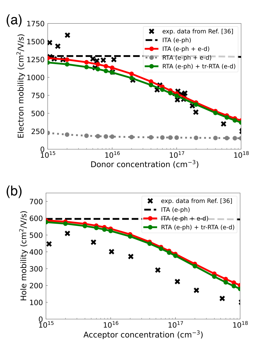
We first focus on the dependence of the electron and hole mobilities on doping concentration.
Figure 3(a) compares the computed electron mobility with experiments [38] for P-doped Si at K.
The phonon-limited mobility, computed using the ITA without -d interactions, is independent of donor concentration and overestimates the experimental mobility values at all doping concentrations greater than 1015 cm-3.
Including both -ph and -d ionized-impurity scattering within the ITA allows us to predict the experimental data with a high accuracy up to cm-3. Greater doping concentrations that modify the band structure [39] are not studied here.
We also find that using the RTA for -ph plus tr-RTA for -d scattering provides electron mobilities close to the full-ITA solution (with -ph plus -d interactions) for a greatly reduced computational cost.
Conversely, the RTA for both -ph and -d scattering (i.e., without the cosine factors in the -d scattering) significantly underestimates the mobility.
We obtain analogous results for hole carriers in B-doped Si at K [Fig. 3(b)]. Comparing the computed hole mobility with experimental data [38] again shows that full ITA calculations
can correctly predict the dependence of the mobility on doping, providing results in agreement with experiment.
Similar results are obtained with -ph RTA plus -d tr-RTA calculations. For hole carriers, we find a greater discrepancy with experiment (a factor of 1.22x) than for electrons. Improving the effective masses (for example, using GW or experimental values [16]) and accounting for spin-orbit coupling would refine the results.
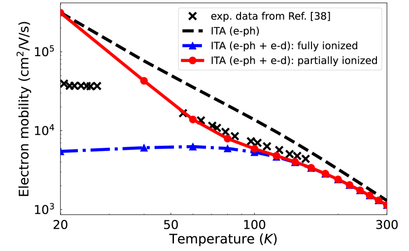
Finally, we analyze the temperature dependence of the mobility for a fixed doping concentration.
For shallow donors, the impurities are fully ionized at higher temperatures, but only partially ionized or in their charge-neutral state at lower temperatures, posing additional challenges to our calculations.
Figure 4 shows the temperature-dependent electron mobility in P-doped Si; one set of results assumes fully-ionized impurities and the other takes into account partial impurity ionization as described in Supplemental Material [22].
When accounting for partial ionization, our full ITA calculations with both -ph and -d scattering can accurately predict the experimental mobility [40] above K. However, scattering from the neutral P donor in our calculation is too weak to reproduce the measured residual mobility below 50 K.
This result suggests that the mobility below K may be limited by scattering mechanisms not included here. In particular, higher-order neutral-impurity scattering, which is usually neglected in the interpretation of transport experiments, has been shown to be important at low temperature [41].
Our results reinforce the hypothesis that low-temperature transport may be governed by higher-order -d interactions with impurities in their charge-neutral state. A recent quantitative study using the T-matrix approach [42] concluded that higher-order -d scattering rates for neutral defects can differ by orders of magnitude from the lowest-order -d interactions employed here. More work is needed to include such higher-order effects in our transport calculations.
Our results highlight the need to carefully take into account partial dopant ionization.
In Fig. 4, our full-ITA calculation assuming fully ionized donors gives electron mobilities well below the experimental values between 50100 K, and saturate to a residual mobility an order of magnitude lower than experiment below K. The temperature trend of the mobility betweeen 50100 K, where partial ionization is essential, is completely missed.
The framework presented in this work lends itself to various applications beyond our proof-of-concept study of doped Si. Although we focused on shallow defects, our method can also be applied to deep-level defects, a topic of great relevance for halide perovskites and narrow-gap semiconductors. Both bulk and two-dimensional (2D) materials can be treated, provided the Coulomb potential in the 2D material is modified to account for the different dimensionality. Among other systems, van der Waals materials and heterostructures [43], as well as interfaces between bulk materials, would greatly benefit from detailed studies of how defects impact charge transport. Extensions to include higher-order neutral impurity scattering, for example with the T-matrix approach, will be considered in future work.
In summary, we developed a rigorous and practical first-principles approach to compute -d interactions due to ionized impurities or other charged defects. Our method can take into account the atomic structure of the defects, the spatially-varying Bloch wave functions, and an arbitrary, anisotropic and multi-valley band structure. This framework makes it possible to capture important defect physics in ab initio calculations of electron dynamics. Our work enables studies of transport from low to high temperatures in doped semiconductors and oxides without any fitting or empirical parameters.
Acknowledgements.
This work was supported by the Air Force Office of Scientific Research through the Young Investigator Program Grant FA9550-18-1-0280. This research used resources of the National Energy Research Scientific Computing Center (NERSC), a U.S. Department of Energy Office of Science User Facility located at Lawrence Berkeley National Laboratory, operated under Contract No. DE-AC02-05CH11231. I-T. L. thanks Dr. Ivan Maliyov and Dr. Cheng-Wei Lee for fruitful discussions.References
- Chattopadhyay and Queisser [1981] D. Chattopadhyay and H. J. Queisser, Electron scattering by ionized impurities in semiconductors, Rev. Mod. Phys. 53, 745 (1981).
- Ridley [2013] B. K. Ridley, Quantum Processes in Semiconductors (Oxford University Press, New York, 2013).
- Lundstrom [2009] M. Lundstrom, Fundamentals of Carrier Transport (Cambridge University Press, New York, 2009).
- Restrepo et al. [2009] O. D. Restrepo, K. Varga, and S. T. Pantelides, First-principles calculations of electron mobilities in silicon: Phonon and Coulomb scattering, Appl. Phys. Lett. 94, 212103 (2009).
- Lu et al. [2019] I.-T. Lu, J.-J. Zhou, and M. Bernardi, Efficient ab initio calculations of electron-defect scattering and defect-limited carrier mobility, Phys. Rev. Mater. 3, 033804 (2019).
- Lu et al. [2020] I.-T. Lu, J. Park, J.-J. Zhou, and M. Bernardi, Ab initio electron-defect interactions using Wannier functions, NPJ Comput. Mater. 6, 1 (2020).
- Bernardi [2016] M. Bernardi, First-principles dynamics of electrons and phonons, Eur. Phys. J. B 89, 239 (2016).
- Zhou and Bernardi [2016] J.-J. Zhou and M. Bernardi, Ab initio electron mobility and polar phonon scattering in GaAs, Phys. Rev. B 94, 201201 (2016).
- Qiu et al. [2015] B. Qiu, Z. Tian, A. Vallabhaneni, B. Liao, J. M. Mendoza, O. D. Restrepo, X. Ruan, and G. Chen, First-principles simulation of electron mean-free-path spectra and thermoelectric properties in silicon, EPL 109, 57006 (2015).
- Ganose et al. [2021] A. M. Ganose, J. Park, A. Faghaninia, R. Woods-Robinson, K. A. Persson, and A. Jain, Efficient calculation of carrier scattering rates from first principles, Nat. Commun. 12, 1 (2021).
- Chaves et al. [2020] A. S. Chaves, A. Antonelli, D. T. Larson, and E. Kaxiras, Boosting the efficiency of ab initio electron-phonon coupling calculations through dual interpolation, Phys. Rev. B 102, 125116 (2020).
- Kaasbjerg et al. [2017] K. Kaasbjerg, J. H. J. Martiny, T. Low, and A.-P. Jauho, Symmetry-forbidden intervalley scattering by atomic defects in monolayer transition-metal dichalcogenides, Phys. Rev. B 96, 241411 (2017).
- Jhalani et al. [2020] V. A. Jhalani, J.-J. Zhou, J. Park, C. E. Dreyer, and M. Bernardi, Piezoelectric electron-phonon interaction from ab initio dynamical quadrupoles: Impact on charge transport in wurtzite GaN, Phys. Rev. Lett. 125, 136602 (2020).
- Zhou et al. [2021] J.-J. Zhou, J. Park, I.-T. Lu, I. Maliyov, X. Tong, and M. Bernardi, Perturbo: A software package for ab initio electron–phonon interactions, charge transport and ultrafast dynamics, Comput. Phys. Commun. 264, 107970 (2021).
- Desai et al. [2021] D. C. Desai, B. Zviazhynski, J.-J. Zhou, and M. Bernardi, Magnetotransport in semiconductors and two-dimensional materials from first principles, Phys. Rev. B 103, L161103 (2021).
- Poncé et al. [2018] S. Poncé, E. R. Margine, and F. Giustino, Towards predictive many-body calculations of phonon-limited carrier mobilities in semiconductors, Phys. Rev. B 97, 121201 (2018).
- Brunin et al. [2020] G. Brunin, H. P. C. Miranda, M. Giantomassi, M. Royo, M. Stengel, M. J. Verstraete, X. Gonze, G.-M. Rignanese, and G. Hautier, Phonon-limited electron mobility in Si, GaAs, and GaP with exact treatment of dynamical quadrupoles, Phys. Rev. B 102, 094308 (2020).
- Van de Walle and Neugebauer [2004] C. G. Van de Walle and J. Neugebauer, First-principles calculations for defects and impurities: Applications to III-nitrides, J. Appl. Phys. 95, 3851 (2004).
- O’Hara et al. [2019] A. O’Hara, B. R. Tuttle, X.-G. Zhang, and S. T. Pantelides, Formation energies of charged defects in two-dimensional materials – resolution of long-standing difficulties, arXiv:1911.11192 (2019).
- Resta [1979] R. Resta, Dielectric behavior of a doped semiconductor, Phys. Rev. B 19, 3022 (1979).
- Ashcroft and Mermin [1976] N. W. Ashcroft and N. D. Mermin, Solid State Physics (Saunders College Publishing, 1976).
- [22] See Supplemental Material at (URL to be added) for additional computational details, Wannier interpolation of the -d matrix elements, and treatment of partially ionized impurities.
- Li [2015] W. Li, Electrical transport limited by electron-phonon coupling from Boltzmann transport equation: An ab initio study of Si, Al, and MoS2, Phys. Rev. B 92, 075405 (2015).
- Ziman [2001] J. M. Ziman, Electrons and Phonons: The Theory of Transport Phenomena in Solids (Oxford University Press, New York, 2001).
- Mahan [2010] G. D. Mahan, Condensed Matter in a Nutshell (Princeton University Press, New York, 2010).
- Li et al. [2016] S.-L. Li, K. Tsukagoshi, E. Orgiu, and P. Samorì, Charge transport and mobility engineering in two-dimensional transition metal chalcogenide semiconductors, Chem. Soc. Rev. 45, 118 (2016).
- Perdew et al. [1996] J. P. Perdew, K. Burke, and M. Ernzerhof, Generalized gradient approximation made simple, Phys. Rev. Lett. 77, 3865 (1996).
- van Setten et al. [2018] M. J. van Setten, M. Giantomassi, E. Bousquet, M. J. Verstraete, D. R. Hamann, X. Gonze, and G. M. Rignanese, The PseudoDojo: Training and grading a 85 element optimized norm-conserving pseudopotential table, Comput. Phys. Commun. 226, 39 (2018).
- Giannozzi et al. [2009] P. Giannozzi, S. Baroni, N. Bonini, M. Calandra, R. Car, C. Cavazzoni, D. Ceresoli, G. L. Chiarotti, M. Cococcioni, I. Dabo, A. D. Corso, S. d. Gironcoli, S. Fabris, G. Fratesi, R. Gebauer, U. Gerstmann, C. Gougoussis, A. Kokalj, M. Lazzeri, L. Martin-Samos, N. Marzari, F. Mauri, R. Mazzarello, S. Paolini, A. Pasquarello, L. Paulatto, C. Sbraccia, S. Scandolo, G. Sclauzero, A. P. Seitsonen, A. Smogunov, P. Umari, and R. M. Wentzcovitch, QUANTUM ESPRESSO: a modular and open-source software project for quantum simulations of materials, J. Phys.: Condens. Matter 21, 395502 (2009).
- [30] DFT calculations on the primitive unit cell of Si use a Å lattice constant and an -point grid. We employ supercells containing atoms, with one Si atom replaced by the impurity dopant, to simulate P-doped and B-doped Si, with the BZ sampled at the -point only. The plane-wave kinetic energy cutoffs are 40 Ry for P-doped and 70 Ry for B-doped Si. The -ph and the -d matrix elements are first computed in the Bloch representation on coarse BZ grids, and then Fourier-transformed to a WF representation and interpolated to fine BZ grids using WF-based interpolation. We use the fine-grid -ph and -d matrix elements to compute the RTs and MFPs, which are fully converged using more than million points in the fine BZ grids. Additional computational details are provided in the Supplemental Material [22].
- Datta [1997] S. Datta, Electronic Transport in Mesoscopic Systems (Cambridge University Press, New York, 1997).
- Kasap and Capper [2017] S. Kasap and P. Capper, Springer Handbook of Electronic and Photonic Materials (Springer, Trento, Italy, 2017).
- Böer and Pohl [2018] K. W. Böer and U. W. Pohl, Semiconductor Physics (Springer, New York, 2018).
- Bernardi et al. [2014] M. Bernardi, D. Vigil-Fowler, J. Lischner, J. B. Neaton, and S. G. Louie, Ab initio study of hot carriers in the first picosecond after sunlight absorption in silicon, Phys. Rev. Lett. 112, 257402 (2014).
- Wei et al. [2008] J. Wei, D. Olaya, B. S. Karasik, S. V. Pereverzev, A. V. Sergeev, and M. E. Gershenson, Ultrasensitive hot-electron nanobolometers for terahertz astrophysics, Nat. Nanotech. 3, 496 (2008).
- Ferry et al. [2020] D. K. Ferry, S. M. Goodnick, V. R. Whiteside, and I. R. Sellers, Challenges, myths, and opportunities in hot carrier solar cells, J. Appl. Phys. 128, 220903 (2020).
- Note [1] A first step in this direction, using methods less advanced than those developed here, was taken in early work by Restrepo et al. [4].
- Jacoboni et al. [1977] C. Jacoboni, C. Canali, G. Ottaviani, and A. Alberigi Quaranta, A review of some charge transport properties of silicon, Solid State Electron. 20, 77 (1977).
- Altermatt et al. [2006] P. P. Altermatt, A. Schenk, and G. Heiser, A simulation model for the density of states and for incomplete ionization in crystalline silicon. I. Establishing the model in Si:P, J. Appl. Phys. 100, 113714 (2006).
- Norton et al. [1973] P. Norton, T. Braggins, and H. Levinstein, Impurity and lattice scattering parameters as determined from Hall and mobility analysis in -type silicon, Phys. Rev. B 8, 5632 (1973).
- Szmulowicz [1986] F. Szmulowicz, Calculation of the mobility and the Hall factor for doped p-type silicon, Phys. Rev. B 34, 4031 (1986).
- Kaasbjerg [2020] K. Kaasbjerg, Atomistic -matrix theory of disordered two-dimensional materials: Bound states, spectral properties, quasiparticle scattering, and transport, Phys. Rev. B 101, 045433 (2020).
- Novoselov et al. [2016] K. S. Novoselov, A. Mishchenko, A. Carvalho, and A. H. C. Neto, 2D materials and van der waals heterostructures, Science 353, aac9439 (2016).