Target-wavelength-trimmed second harmonic generation with gallium phosphide-on-nitride ring resonators
Abstract
We demonstrate post-fabrication target-wavelength trimming with a gallium phosphide on silicon nitride integrated photonic platform using controlled electron-beam exposure of hydrogen silsesquioxane cladding. A linear relationship between the electron-beam exposure dose and resonant wavelength red-shift enables deterministic, individual trimming of multiple devices on the same chip to within 30 pm of a single target wavelength. Second harmonic generation from telecom to near infrared at a target wavelength is shown in multiple devices with quality factors on the order of . Post-fabrication tuning is an essential tool for targeted wavelength applications including quantum frequency conversion.
1 Introduction
Nanophotonic devices have transformed frequency conversion processes, enabling conversion efficiencies orders of magnitude higher than in bulk materials by confining light and controlling mode dispersion. To fully leverage the potential of nanophotonic platforms for frequency conversion, multi-resonant devices are desirable; for example, in a nonlinear media, doubly resonant devices for second-harmonic generation (SHG) and parametric down-conversion (PDC) and triply resonant devices for difference- and sum-frequency generation. Moreover, applications are emerging in which an absolute frequency of one or more interacting fields is required. Examples of this include PDC entangled photon sources for optical quantum computing [1, 2, 3, 4] and frequency conversion of single visible or NIR photons, emitted by ions or solid-state defects, for long-distance fiber transmission [5, 6, 7, 8, 9]. Toward this latter application, multi-resonant frequency conversion of photons to/from the telecom band has been demonstrated in nanophotonic structures fabricated from non-linear materials such as gallium phosphide (GaP) [10], aluminum nitride [11], lithium niobate [12, 13] and silicon nitride [14, 15]. However, tight fabrication tolerances for such devices typically cause resonant wavelengths to differ significantly from their designed values, presenting a challenge for practical device implementation. Here we introduce a promising technique for post-fabrication nanoscale control of photonic resonances to address this challenge via electron-beam modification of hydrogen silsesquioxane (HSQ) cladding.
Generally, photonic resonators can be tuned by altering the physical dimensions or optical properties of the structure. For a ring resonator, tuning variables include ring width and height, resonator refractive index, and cladding refractive index. Resonances may be either tuned via processes that require constant active control (e.g. temperature [16, 17], electric field [18, 19]) or trimmed via processes that permanently change device parameters (e.g. etching [20, 21, 22], introducing strain [23, 24], modification of cladding material [25, 26, 27, 28]). Resonant wavelength modification of ring resonators for frequency conversion processes presents a particularly complex challenge due to the simultaneous involvement of multiple wavelengths. Any tuning or trimming process will cause a shift in both absolute resonant wavelength and relative spacing between the two or more required resonances. Thus, realizing multiple independent tuning mechanisms and/or developing techniques which offer the spatial resolution to preferentially tune certain resonator modes are particularly interesting. Further, a tuning mechanism that can be readily integrated into a well established fabrication process is preferred.
HSQ is heavily utilized for high-resolution electron-beam lithography [29, 30] of photonic devices and is fully compatible with most materials and fabrication processes. Prior studies have investigated the utility of HSQ for resonance tuning using thermal annealing [31] to convert the cage-like structure of uncured HSQ into a denser cross-linked silica structure, increasing the index of refraction from n = 1.45 to n = 1.51. Similarly, localized laser[26] and in situ[25] annealing of HSQ on individual silicon micro-ring resonators has been utilized to shift resonances by up to 2 nm. Both techniques involve heating the devices to high temperatures, thus limiting integration of III-V non-linear photonic materials such as GaAs and GaP. Additionally, long-term, the spatial resolution afforded by thermal processes will be inadequate for multi-resonance frequency conversion applications. High-energy electron-beam exposure allows high spatial and tuning resolution [28]. In this work we investigate the utility of HSQ electron-beam exposure as a method for high-resolution, post-fabrication, single device trimming, with the potential for mode-selective trimming. Electron-beam exposure of HSQ has been shown to induce cross-linking similar to thermal annealing, while high exposure intensity enables further refractive index tuning (up to ) via the formation of silicon-rich SiO2 [32, 33]. Our results indicate that the induced wavelength shift is linearly dependent on the electron-beam exposure dose, with an observed trimming range of 5 nm for the applied doses. We demonstrate high spatial and tuning resolution, resonance stability, and minimal impact on device quality factor (Q), making HSQ electron-beam trimming a promising candidate for use in quantum frequency conversion applications. Finally, we demonstrate successful target-wavelength second harmonic generation with multiple devices and provide an outlook toward utilizing this technology for simultaneous multiple resonance tuning.
2 Resonator design, fabrication and testing
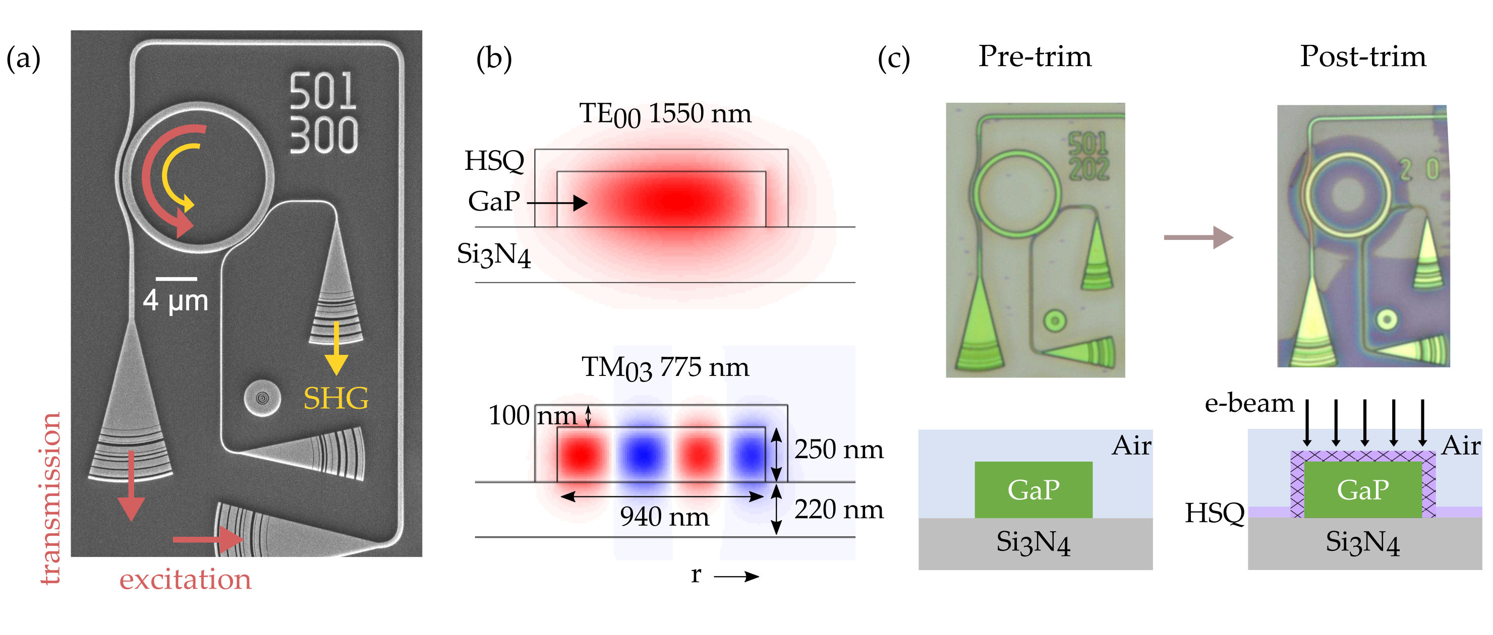
The ring resonators were designed and fabricated in a 250 nm (100) GaP photonic layer on an epiwafer substrate with 220 nm LPCVD silicon nitride on 4 µm silicon oxide on silicon. A ring radius of 7.77 µm and width of 940 nm were selected to satisfy a quasi-phase matching condition for a TE00 fundamental mode and TM03 second harmonic (SH) mode at and , respectively [10]. Each ring mode is evanescently coupled to a different input/output waveguide leading to a pair of cross-polarized grating couplers. A device SEM image and schematic are shown in Fig. 1a, with the relevant mode profiles in Fig. 1b. Additional design details can be found in Appendix A1.
Eigenmode simulations of the ring resonator predict that an increment in refractive index of in a 100 nm thick conformal HSQ cladding will red-shift the resonant wavelength of the fundamental mode by 2.98 nm and SH mode by 1.07 nm. With changes in HSQ refractive index as high as 0.22 reported [32, 33], the predicted trimming range is capable of compensating for typical device-to-device fabrication variations.
To fabricate the structure, the 250 nm GaP layer was released from a GaP substrate by etching an intermediate sacrificial layer with dilute HF. The GaP was then transferred to the Si3N4-on-SiO2/Si substrate using a wet transfer process [34, 35, 36, 10]. Electron-beam lithography using HSQ resist and subsequent plasma reactive-ion-etching (RIE) of the GaP layer forms the photonic devices. Two chips (A and B) were fabricated with identical device dimensions. After fabrication, a layer of developed HSQ mask remains. This HSQ layer is removed with a vapor-HF etch, enabling the spin-on of a new conformal coating of HSQ for the resonance trimming process. After HSQ spin-on, each device was trimmed by exposing a donut-shaped region extending 1 µm beyond the inner and outer device radii at a beam voltage of 5 keV (Fig. 1c). Further details of the fabrication are provided in Appendix A2. The fabrication process is compatible with diamond substrates for GaP-on-diamond or GaAs-on-diamond photonic circuits integrated with solid-state defects [35, 36, 37].
The fundamental resonances of individual devices were identified by sweeping a continuous-wave telecom laser (1530 to 1565 nm) and detecting transmission spectra using a InGaAs photodiode. In the visible band a supercontinuum laser (550 to 1350 nm) was used for excitation and the transmission spectra is detected with a grating spectrometer. The excitation polarization was set to excite TE (1550 nm) or TM (775 nm) modes, as depicted in Fig. 1a. Scattered excitation light was filtered out of the collection path via polarization and spatial filtering. Chip-A exhibited resonances with Q-factors of 7 2.2 103. Chip-B exhibited narrower resonances with Q-factors of 3 1.7 104.
3 HSQ target-wavelength trimming
The first goal is to establish a relationship between exposure dose and resonant wavelength shift to deterministically tune the resonant wavelength of individual devices on-chip. Approximately 24 hours after HSQ spin-on, 13 devices (chip-A) were selected for a dose-test and exposed with electron-beam lithography. Three devices each received doses of 1000, 1750, and 2500 µC/cm2 respectively and four devices received no exposure. Transmission spectra of one specific fundamental mode taken before and after exposure show a linear relationship between resonance shift and exposure dose (Fig. 2a). On average, the exposed devices exhibit a tuning rate (red-shift) of 1.4 0.1 pm/µC/cm2, with the maximum tested dose (2500 µC/cm2) giving an average shift of 3.08 nm.
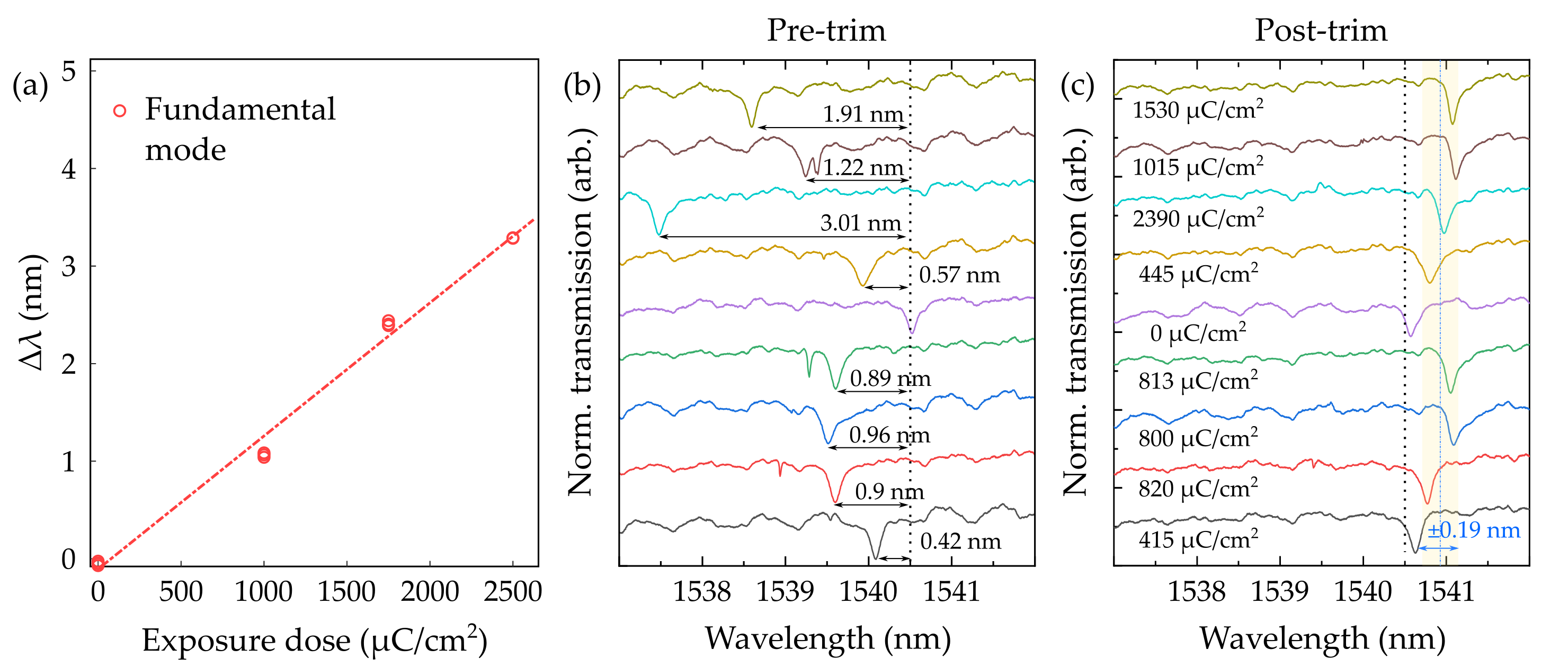
In the next step, a set of nine identically designed devices were identified (Fig. 2b) with initial resonances near nm to trim to mutual resonance. Before trimming, the spread of resonant wavelengths was measured to be 3 nm. We used the above linear dose-shift relationship to determine the necessary exposure dose for targeted trimming of each device resonance to nm. With a single exposure of each device, all resonances were trimmed to the target wavelength with an offset of 0.410.19 nm (Fig. 2c).
Post-tuning analysis (Appendix A3) of the transmission spectra determined that the tuning rate is different for various families of modes supported by the ring. The highest observed shift was 4.92 nm (Fig. A1a, mode-1). The significant mode-sensitivity suggests deterministic inter-modal control could be developed within this platform. Further, we observed an average post-trim resonance drift of 10.6 pm/day (corresponding to 0.7% of average trimmed red-shift or 5% of the average target resonance linewidth) over 12 days. This minor drift followed a non-monotonic trend for all tested devices. The source of the post-exposure drift requires further investigation.
4 Target-wavelength-trimmed SHG
In a second experiment (chip-B), we expanded the scope of our dose-test to incorporate both the fundamental and SH modes. Using the same dose-test procedure, a linear dose-shift relationship is found for the fundamental mode with a nearly identical tuning rate (1.2 0.1 pm/µC/cm2) to the chip-A dose-test. The largest dose (2500 µC/cm2) corresponds to an average shift of 3.0 nm. This matches the simulated resonance shift for a cladding index change of , which is reasonable for the large electron-beam exposure dose [32]. A linear dose-shift relationship (0.5 0.2 pm/µC/cm2) is also established for the SH mode (Fig. 3a). Due to the highly multi-mode nature of the ring at 775 nm, difficulty in consistently identifying radial modes prevented us from accurately determining the mode-specific trimming rate of the targeted SH mode. Thus, we focus on HSQ target trimming of the fundamental mode to demonstrate target-wavelength-trimmed SHG in multiple devices.
We selected three nominally identical devices with telecom resonances that exhibited strong SH conversion. The initial spread of resonances was 1.11 nm. Each device was exposed to a calibrated HSQ electron-beam dose for trimming to a target wavelength of nm. All three devices were trimmed to within of the target wavelength (Fig. 3b). The strong temperature dependence of the SHG signal (Fig. 3c), indicates that the devices were close to quasi-phase matched double resonance after the trimming process. The SH and fundamental resonances red-shift at different rates with increasing temperature, causing the SHG conversion efficiency to peak as the SH resonance tunes into and out of double resonance with the fundamental. All three devices gain some double-resonant SHG enhancement at the target wavelength (1533.75 nm), but due to remaining variations in the SH resonant wavelength after the HSQ exposure trimming, each resonator reaches its maximum SHG efficiency at a slightly different temperature and wavelength.
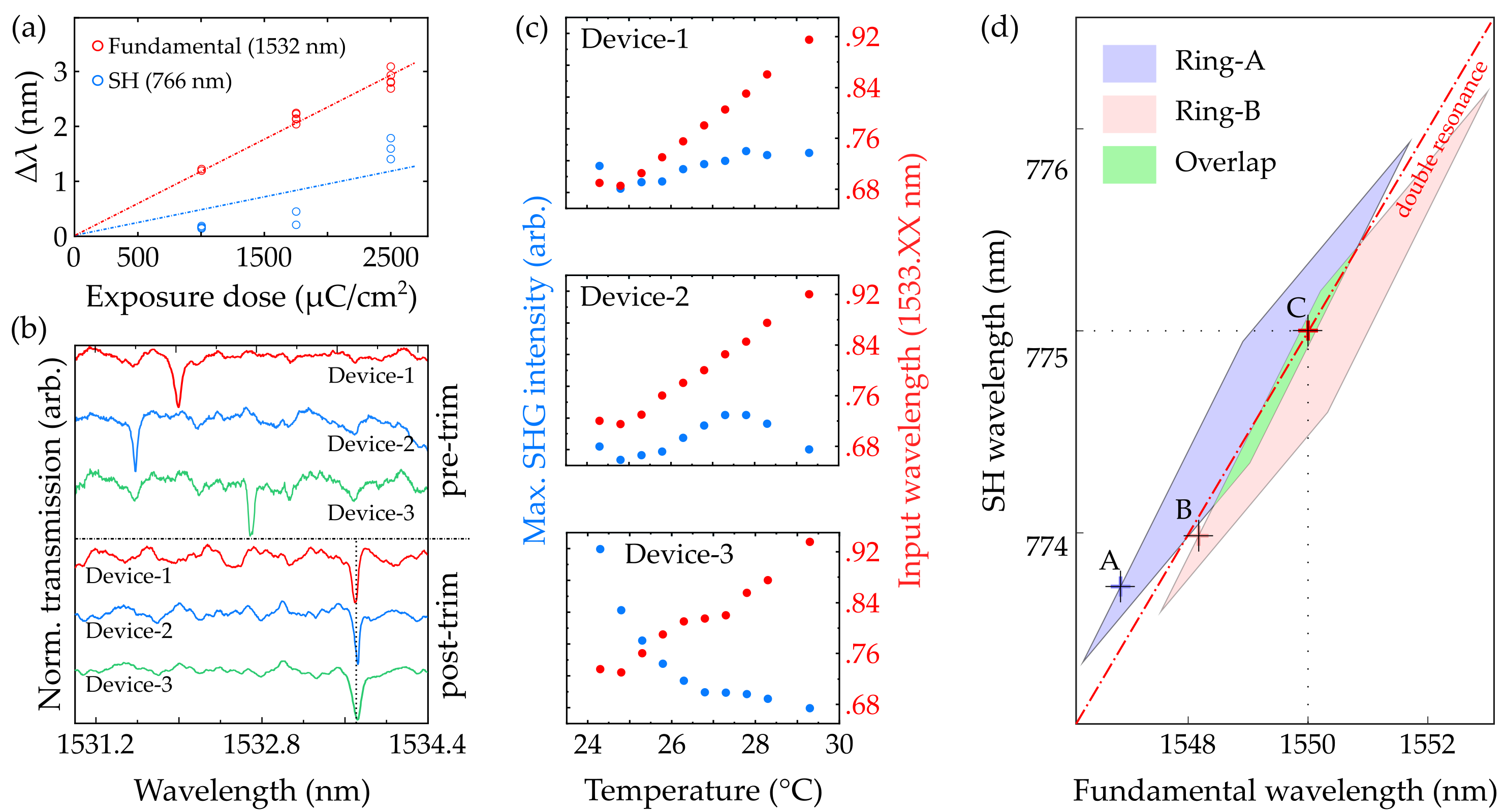
SHG efficiency is also very sensitive to the Q-factors of the resonant modes. The narrow resonances observed on chip-B enable us to investigate the effect of trimming on the fundamental mode Q-factor. Initially the average Q-factor for 15 devices was 3 1.7104. The Q-factor is observed to both decrease and increase with the average Q decreasing by 5.1 6.1103 after exposure. It is likely that the majority of this variation in Q can be attributed to exposure of the coupling region, altering the coupling-Q as described in Appendix A1. An exposure pattern that avoids the coupling region could maintain the device Q through the trimming process. Further, selective exposure of the coupling regions could be utilized to tune devices to the critical-coupling regime in addition to resonant wavelength trimming.
5 Outlook and Conclusion
In this work we demonstrated that HSQ exposure is a promising post-fabrication trimming method for photonic resonators. With a simple calibration process, we target-wavelength trim a large set of identically designed devices with typical post-fabrication variations. HSQ trimming will be an important tool in the larger effort towards target-wavelength frequency conversion. For example, combined with temperature tuning, HSQ trimming should enable dual target-wavelength trimming for doubly resonant quasi-phase matched frequency conversion processes. The devices in this work that were trimmed to correct variance at the telecom wavelength at room temperature still had some variance in the SH resonance, resulting in maximum SHG conversion at different temperatures and wavelengths. By taking the effect of temperature tuning into account when selecting exposure doses, Fig. 3d illustrates how multiple resonators could be trimmed to provide their maximum SHG conversion efficiency at the same target wavelength. Two simulated devices (A, B) with fundamental wavelengths differing by 1.3 nm at room temperature and at their optimal SHG temperatures can be target wavelength tuned within the green dose-temperature area. A third independent tuning mechanism will be required to achieve optimal efficiency for a specific sum- or difference-frequency conversion process needed for quantum frequency conversion applications.
The attractive properties of HSQ exposure trimming include tuning range, resolution and precision, low post-trim drift and minimal effect on quality factor. We expect that additional process development will further improve the accuracy and precision. Better mode identification will reduce uncertainty in mode-specific trimming rates enabling the implementation of multiple tuning mechanisms. Improved understanding of sources of drift will allow us to design for or mitigate post-trim resonant shifts. The spatial resolution afforded by electron-beam lithography for HSQ trimming creates potential for applications beyond resonance shifting. Selective exposure of coupling regions could allow post-fabrication fine tuning of coupling Q. Other works have shown that periodic nanometer-scale variations along the ring inner radius can target specific modes for mode-splitting [38]. Electron-beam lithography-based trimming makes target mode trimming and splitting a realistic opportunity. We have shown HSQ exposure to be a simple and effective post fabrication trimming technique. With further development it stands to become a process widely utilized by the photonics community.
Appendix
A1 Device design and simulation details
The ring resonators were designed using bent-waveguide eigenmode simulations in Lumerical MODE. Using ring radius and width as design variables, the resonator was optimized to maximize nonlinear overlap while satisfying the mode polarization and quasi-phase matching (QPM) requirements imposed by the zincblende crystal symmetry and (100)-normal orientation of the GaP photonic layer [10, 39, 40]. At each design point, the target modes ( at and at ) were simulated in a ring cross section. The nonlinear overlap was calculated from the mode profiles, along with fractional azimuthal mode numbers for each mode, which are used to check the QPM condition . Integer azimuthal mode numbers at the simulated wavelengths are preferred, but not required; a design with non-integer is expected to have QPM modes that are near double resonance at wavelengths that are not exactly 1550 nm and 775 nm in ambient conditions, which is acceptable if within the tolerance of our tuning capabilities. Based on previous experiments in similar material platforms (GaP-on-Diamond, GaP-on-oxide), intrinsic quality factor is expected to be dominated by fabrication-related factors such as sidewall roughness, so the simulated radiative quality factor was not considered for the design process.
The ring resonator coupling regions were designed to provide specific coupling quality factors using a supermode analysis method. For a range of coupling waveguide widths and ring-to-waveguide distances, the target ring and waveguide modes were simulated with each structure alone, and then all guided modes were simulated for the combined structure. Mode overlap between each coupling region mode and the ring/waveguide modes were calculated and used to numerically find the total power transfer from the ring mode to waveguide mode as a function of coupling region length. The coupling quality factor was derived from the simulated free spectral range of the resonator mode and the field coupling coefficient from a single pass through the coupling region:
| (1) |
To provide a consistent interface to the rest of the coupling photonic circuit, a constant waveguide width and propagation length was selected for each ring mode’s coupling region, with only the separation distance varied to set .
Coupling quality factor depends significantly on how well the HSQ fills the space between the ring and the waveguide, as well as HSQ exposure dose; the coupling regions were simulated with a 100 nm conformal HSQ layer. The telecom ring mode is coupled to a 440 nm wide waveguide wrapped around a arc of the ring, and the SH mode is coupled to a 120 nm waveguide with a wrap. For the telecom mode, a ring-to-waveguide gap distance of 240 nm gives with increasing ebeam exposure, and a distance of 360 nm gives . For the SH mode, a gap distance of 120 nm gives , and 160 nm gives .
The grating couplers were designed to provide coupling to free space with minimal footprint and low back reflections. For each wavelength band and polarization, an aperiodic grating coupler design was found using a sampled hill climbing optimization algorithm with a simplified model of grating behavior as an objective function. The performance of the final design was verified with a 3D FDTD simulation. To suppress on-chip back reflections, which cause Fabry-Perot interference patterns in transmission spectra, the grating designs were implemented as elliptically-shaped focusing grating couplers. The grating notches are shaped as sections of progressively larger ellipses with one focus centered on the end of the waveguide. Back reflections from the waveguide are directed toward the second focus of the ellipse instead of going back into the waveguide mode [41]. The design variables used for the elliptical grating were: eccentricity, the angle between waveguide and major axis, the arc angle of the elliptical section, and major axis length of first grating notch. Designs were evaluated with 3D FDTD simulations to find a combination of parameters that sufficiently suppresses back reflection in the the same mode while maintaining a reasonable spot shape for light scattered into free space.
A2 Fabrication details
The GaP material used for the photonics layer was grown by molecular beam epitaxy on a 300 nm sacrificial layer on a GaP substrate. This epitaxial GaP layer was released in 2% HF solution, followed by a H2O rinse and wet transfer to the nitride substrate. To improve GaP adhesion, prior to transfer, a 5 nm layer of SiO2 was thermally evaporated onto the substrate, which was then treated with hexamethyldisilizane vapor. The transferred GaP was allowed to dry overnight on a hotplate at 80 ∘C. Electron beam lithography (JEOL-6300, 100 kV, 1 nA beam current) was utilized to pattern the designed photonic structures on a thin (150 nm) HSQ resist layer on top of the GaP-on-nitride stack. Multiple arrays of devices were patterned with the resonator and coupling region dimensions varying across the pattern to compensate for fabrication variations. A reactive-ion etch (RIE) step (3.0 mTorr, 45 W RF, 60 W ICP, 235 V DC-bias, 1.0/6.0/3.0 sccm Cl2/Ar/N2 flow) was used to etch the GaP layer. The residual HSQ mask had to be removed. Initial attempts at HSQ removal using a dilute HF (0.5%) dip revealed low adhesion of the GaP devices to the substrate: stiction from the wet process damaged the waveguide coupling regions. Thus, a HF vapor-etch process was investigated. After the successful HSQ vapor-etch, the chip was heated to 200 ∘C for 5 min to remove etch byproducts. This provided a clean surface for a 150 nm layer of HSQ electron-beam resist that was spun-on and exposed for device trimming. The thickness of this HSQ layer is expected to shrink by up to 33% due to e-beam exposure [32].
A3 Post-tuning analysis
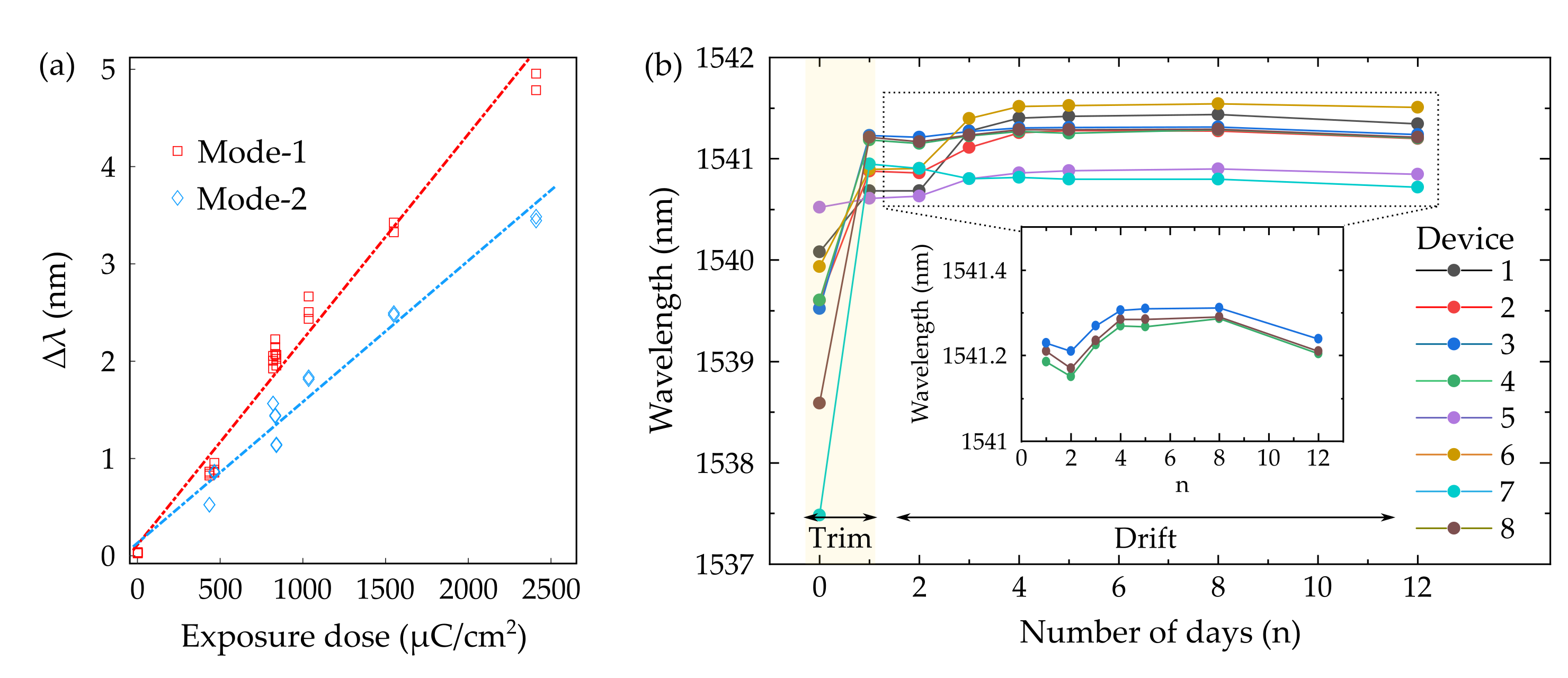
The dose-shift relationship is dependent on the overlap of the target mode with the surrounding cladding. Analysis of the chip-A trim-test data (Fig. A1a) reveals that two families of modes were observed in the transmission spectra (1530 to 1565 nm) with significantly different tuning rates. Mode-1 (FSR = 13.61 0.14 nm) exhibits a sensitivity of 2.11 pm/µC/cm2, and mode-2 (FSR = 12.91 0.05 nm) exhibits a lower sensitivity of 1.45 pm/µC/cm2. From simulations, the fundamental TE00 mode is expected to have an FSR14.7 nm. Given the smaller observed FSR, we suspect both these families of resonances are higher order hybrid TE01/TM00 modes. Simulations show these hybrid modes tune about twice as fast as the fundamental mode, with a change in HSQ cladding index of 0.1 shifting the wavelength by about 6.25 nm and 7.32 nm respectively instead of 2.98 nm.
To monitor the temporal stability of the trimming process, after HSQ exposure, room temperature transmission spectra of eight identically designed devices were periodically collected over a 12 day period. Devices 1, 2, 6 and 7 were re-exposed for fine target wavelength trimming. Therefore, we only included the remaining devices for detailed analysis of the resonance shift. One possible reason for the observed shift could be the change in refractive index of the cladding over time (possibly from uptake of ambient moisture by the exposed HSQ [26, 25]) and further investigation is required for identification of the source of the drift.
Funding
Acknowledgments This material is based upon work supported by the National Science Foundation under Grants EFMA-1640986 (photonic design and fabrication) and U.S. Department of Energy, Office of Science, National Quantum Information Science Research Centers, Co-design Center for Quantum Advantage (C2QA) under contract number DE-SC0012704 (HSQ tuning and testing). The photonic devices were fabricated at the Washington Nanofabrication Facility, a National Nanotechnology Coordinated Infrastructure (NNCI) site at the University of Washington which is supported in part by funds from the National Science Foundation (awards NNCI-1542101, 1337840 and 0335765).
Disclosures The authors declare that there are no conflicts of interest related to this article.
Data Availability Statement Data underlying the results presented in this paper are not publicly available at this time but may be obtained from the authors upon reasonable request.
References
- [1] P. G. Kwiat, E. Waks, A. G. White, I. Appelbaum, and P. H. Eberhard, “Ultrabright source of polarization-entangled photons,” \JournalTitlePhysical Review A 60, R773 (1999).
- [2] P. J. Mosley, J. S. Lundeen, B. J. Smith, P. Wasylczyk, A. B. U’Ren, C. Silberhorn, and I. A. Walmsley, “Heralded generation of ultrafast single photons in pure quantum states,” \JournalTitlePhysical Review Letters 100, 133601 (2008).
- [3] X.-C. Yao, T.-X. Wang, P. Xu, H. Lu, G.-S. Pan, X.-H. Bao, C.-Z. Peng, C.-Y. Lu, Y.-A. Chen, and J.-W. Pan, “Observation of eight-photon entanglement,” \JournalTitleNature photonics 6, 225–228 (2012).
- [4] Y. Wang, K. D. Jöns, and Z. Sun, “Integrated photon-pair sources with nonlinear optics,” \JournalTitleApplied Physics Reviews 8, 011314 (2021).
- [5] J. D. Siverns, J. Hannegan, and Q. Quraishi, “Neutral-atom wavelength-compatible 780 nm single photons from a trapped ion via quantum frequency conversion,” \JournalTitlePhysical Review Applied 11, 014044 (2019).
- [6] X. Lu, Q. Li, D. A. Westly, G. Moille, A. Singh, V. Anant, and K. Srinivasan, “Chip-integrated visible–telecom entangled photon pair source for quantum communication,” \JournalTitleNature physics 15, 373–381 (2019).
- [7] P. Kumar, “Quantum frequency conversion,” \JournalTitleOptics letters 15, 1476–1478 (1990).
- [8] M. Bock, P. Eich, S. Kucera, M. Kreis, A. Lenhard, C. Becher, and J. Eschner, “High-fidelity entanglement between a trapped ion and a telecom photon via quantum frequency conversion,” \JournalTitleNature communications 9, 1–7 (2018).
- [9] S. Zaske, A. Lenhard, C. A. Keßler, J. Kettler, C. Hepp, C. Arend, R. Albrecht, W.-M. Schulz, M. Jetter, P. Michler et al., “Visible-to-telecom quantum frequency conversion of light from a single quantum emitter,” \JournalTitlePhysical review letters 109, 147404 (2012).
- [10] A. D. Logan, M. Gould, E. R. Schmidgall, K. Hestroffer, Z. Lin, W. Jin, A. Majumdar, F. Hatami, A. W. Rodriguez, and K.-M. C. Fu, “400%/w second harmonic conversion efficiency in 14 m-diameter gallium phosphide-on-oxide resonators,” \JournalTitleOptics express 26, 33687–33699 (2018).
- [11] A. W. Bruch, X. Liu, X. Guo, J. B. Surya, Z. Gong, L. Zhang, J. Wang, J. Yan, and H. X. Tang, “17 000%/w second-harmonic conversion efficiency in single-crystalline aluminum nitride microresonators,” \JournalTitleApplied Physics Letters 113, 131102 (2018).
- [12] A. Rao, K. Abdelsalam, T. Sjaardema, A. Honardoost, G. F. Camacho-Gonzalez, and S. Fathpour, “Actively-monitored periodic-poling in thin-film lithium niobate photonic waveguides with ultrahigh nonlinear conversion efficiency of 4600% w- 1 cm- 2,” \JournalTitleOptics express 27, 25920–25930 (2019).
- [13] J.-Y. Chen, Z.-H. Ma, Y. M. Sua, Z. Li, C. Tang, and Y.-P. Huang, “Ultra-efficient frequency conversion in quasi-phase-matched lithium niobate microrings,” \JournalTitleOptica 6, 1244–1245 (2019).
- [14] Y. Liu, M. Davanço, V. Aksyuk, and K. Srinivasan, “Electromagnetically induced transparency and wideband wavelength conversion in silicon nitride microdisk optomechanical resonators,” \JournalTitlePhysical review letters 110, 223603 (2013).
- [15] X. Lu, G. Moille, Q. Li, D. A. Westly, A. Singh, A. Rao, S.-P. Yu, T. C. Briles, S. B. Papp, and K. Srinivasan, “Efficient telecom-to-visible spectral translation through ultralow power nonlinear nanophotonics,” \JournalTitleNature Photonics 13, 593–601 (2019).
- [16] P. Dong, S. Liao, D. Feng, H. Liang, D. Zheng, R. Shafiiha, C.-C. Kung, W. Qian, G. Li, X. Zheng, A. V. Krishnamoorthy, and M. Asghari, “Low vpp, ultralow-energy, compact, high-speed silicon electro-optic modulator,” \JournalTitleOptics Express 17 (2009).
- [17] L. Koehler, P. Chevalier, E. Shim, B. Desiatov, A. Shams-Ansari, M. Piccardo, Y. Okawachi, M. Yu, M. Loncar, M. Lipson, A. L. Gaeta, and F. Capasso, “Direct thermo-optical tuning of silicon microresonators for the mid-infrared,” \JournalTitleOptics Express 26 (2018).
- [18] H. Jung, K. Y. Fong, C. Xiong, and H. X. Tang, “Electrical tuning and switching of an optical frequency comb generated in aluminum nitride microring resonators,” \JournalTitleOptics Letters 39 (2014).
- [19] H. Shen, M. H. Khan, L. Fan, L. Zhao, Y. Xuan, J. Ouyang, L. T. Varghese, and M. Qi, “Eight-channel reconfigurable microring filters with tunable frequency, extinction ratio and bandwidth,” \JournalTitleOptics express 18, 18067–18076 (2010).
- [20] K. Hennessy, A. Badolato, A. Tamboli, P. M. Petroff, E. Hu, M. Atatüre, J. Dreiser, and A. Imamoǧlu, “Tuning photonic crystal nanocavity modes by wet chemical digital etching,” \JournalTitleApplied Physics Letters 87 (2005).
- [21] X. Lu, G. Moille, Q. Li, D. A. Westly, A. Singh, A. Rao, S. P. Yu, T. C. Briles, S. B. Papp, and K. Srinivasan, “Efficient telecom-to-visible spectral translation through ultralow power nonlinear nanophotonics,” \JournalTitleNature Photonics 13 (2019).
- [22] A. H. Atabaki, A. A. Eftekhar, M. Askari, and A. Adibi, “Accurate post-fabrication trimming of ultra-compact resonators on silicon,” \JournalTitleOptics express 21, 14139–14145 (2013).
- [23] M. M. Milosevic, X. Chen, W. Cao, A. F. Runge, Y. Franz, C. G. Littlejohns, S. Mailis, A. C. Peacock, D. J. Thomson, and G. T. Reed, “Ion implantation in silicon for trimming the operating wavelength of ring resonators,” \JournalTitleIEEE Journal of Selected Topics in Quantum Electronics 24, 1–7 (2018).
- [24] J. Schrauwen, D. Van Thourhout, and R. Baets, “Trimming of silicon ring resonator by electron beam induced compaction and strain,” \JournalTitleOptics express 16, 3738–3743 (2008).
- [25] S. Spector, J. M. Knecht, and P. W. Juodawlkis, “Localized in situ cladding annealing for post-fabrication trimming of silicon photonic integrated circuits,” \JournalTitleOptics express 24, 5996–6003 (2016).
- [26] V. Biryukova, G. J. Sharp, C. Klitis, and M. Sorel, “Trimming of silicon-on-insulator ring-resonators via localized laser annealing,” \JournalTitleOptics express 28, 11156–11164 (2020).
- [27] L. Zhou, K. Okamoto, and S. Yoo, “Athermalizing and trimming of slotted silicon microring resonators with uv-sensitive pmma upper-cladding,” \JournalTitleIEEE Photonics Technology Letters 21, 1175–1177 (2009).
- [28] S. Prorok, A. Y. Petrov, M. Eich, J. Luo, and A. K.-Y. Jen, “Trimming of high-q-factor silicon ring resonators by electron beam bleaching,” \JournalTitleOptics letters 37, 3114–3116 (2012).
- [29] A. Grigorescu and C. Hagen, “Resists for sub-20-nm electron beam lithography with a focus on hsq: state of the art,” \JournalTitleNanotechnology 20, 292001 (2009).
- [30] V. R. Manfrinato, F. E. Camino, A. Stein, L. Zhang, M. Lu, E. A. Stach, and C. T. Black, “Patterning si at the 1 nm length scale with aberration-corrected electron-beam lithography: Tuning of plasmonic properties by design,” \JournalTitleAdvanced Functional Materials 29, 1903429 (2019).
- [31] C.-C. Yang and W.-C. Chen, “The structures and properties of hydrogen silsesquioxane (hsq) films produced by thermal curing,” \JournalTitleJournal of Materials Chemistry 12, 1138–1141 (2002).
- [32] H.-J. Lee, J. Goo, S.-H. Kim, J.-G. Hong, H.-D. Lee, H.-K. Kang, S.-I. Lee, and M. Y. Lee, “A new, low-thermal-budget planarization scheme for pre-metal dielectric using electron-beam cured hydrogen silsesquioxane in device,” \JournalTitleJapanese Journal of Applied Physics 39, 3924 (2000).
- [33] S. Choi, M. J. Word, V. Kumar, and I. Adesida, “Comparative study of thermally cured and electron-beam-exposed hydrogen silsesquioxane resists,” \JournalTitleJournal of Vacuum Science & Technology B: Microelectronics and Nanometer Structures Processing, Measurement, and Phenomena 26, 1654–1659 (2008).
- [34] E. Yablonovitch, D. M. Hwang, T. J. Gmitter, L. T. Florez, and J. P. Harbison, “Van der Waals bonding of GaAs epitaxial liftoff films onto arbitrary substrates,” \JournalTitleApplied Physics Letters 56, 2419–2421 (1990).
- [35] M. Gould, E. R. Schmidgall, S. Dadgostar, F. Hatami, and K.-M. C. Fu, “Efficient Extraction of Zero-Phonon-Line Photons from Single Nitrogen-Vacancy Centers in an Integrated GaP-on-Diamond Platform,” \JournalTitlePhysical Review Applied 6, 011001 (2016).
- [36] E. R. Schmidgall, S. Chakravarthi, M. Gould, I. R. Christen, K. Hestroffer, F. Hatami, and K.-M. C. Fu, “Frequency Control of Single Quantum Emitters in Integrated Photonic Circuits,” \JournalTitleNano Letters 18, 1175–1179 (2018).
- [37] D. Huang, A. Abulnaga, S. Welinski, M. Raha, J. D. Thompson, and N. P. de Leon, “Hybrid iii-v diamond photonic platform for quantum nodes based on neutral silicon vacancy centers in diamond,” \JournalTitleOptics Express 29, 9174–9189 (2021).
- [38] X. Lu, A. Rao, G. Moille, D. A. Westly, and K. Srinivasan, “Universal frequency engineering tool for microcavity nonlinear optics: multiple selective mode splitting of whispering-gallery resonances,” \JournalTitlePhotonics Research 8 (2020).
- [39] Z.-F. Bi, A. W. Rodriguez, H. Hashemi, D. Duchesne, M. Loncar, K.-M. Wang, and S. G. Johnson, “High-efficiency second-harmonic generation in doubly-resonant (2) microring resonators,” \JournalTitleOpt. Express 20, 7526–7543 (2012).
- [40] R. Boyd, Nonlinear Optics (Academic, 2008).
- [41] D. Vermeulen, Y. D. Koninck, Y. Li, E. Lambert, W. Bogaerts, R. Baets, and G. Roelkens, “Reflectionless grating couplers for silicon-on-insulator photonic integrated circuits,” \JournalTitleOpt. Express 20, 22278–22283 (2012).