Quantum Hall phase in graphene engineered by interfacial charge coupling
††* These authors contribute equally.†††Corresponding to: jhmao@ucas.ac.cn, yeyu@pku.edu.cn, liujp@shanghaitech.edu.cn, kchang@semi.ac.cn, and vitto.han@gmail.comQuantum Hall effect (QHE), the ground to construct modern conceptual electronic systems with emerging physics [1, 2, 3, 4, 5], is often much influenced by the interplay between the host two-dimensional electron gases and the substrate, sometimes predicted to exhibit exotic topological states [6, 7]. Yet the understanding of the underlying physics and the controllable engineering of this paradigm of interaction remain challenging. Here we demonstrate the observation of an unusual QHE, which differs markedly from the known picture, in graphene samples in contact with an anti-ferromagnetic insulator CrOCl equipped with dual gates. Two distinct QH phases are developed, with the Landau levels in monolayer graphene remaining intact at the conventional phase, but largely distorted for the interfacial-coupling phase. The latter QH phase even presents in the limit of zero magnetic field, with the consequential Landau quantization following a parabolic relation between the displacement field and the magnetic field . This characteristic prevails up to 100 K in a sufficiently wide effective doping range from 0 to 1013 cm-2. Our findings thus open up new routes for manipulating the quantum electronic states, which may find applications in such as quantum metrology.
The QHE is found in a number of solid-state systems to demonstrate topologically protected dissipation-less edge channels with their transversal conductance quantized by , with and being the elementary charge and the Planck constant, respectively [8, 9, 10, 11, 12]. This peculiar behaviour has been crucial for such as the implementation of quantum-based resistance standards with extremely high precision and reproducibility [13]. Among the few known systems manifesting QHE, graphene received special attention for its distinct band structure and the resulting Nth Landau level (LL) at the energy of under a fixed magnetic field . Due to the linear transformation of energy and the square root of carrier density [14, 15, 16], the Landau quantization of conventional graphene in the parameter space of and is defined as the famed Landau fan diagram, with all LLs linearly extrapolated to the charge neutrality point [15, 17, 16].
Interfacial coupling is known to be an important factor to affect the QHE in graphene, usually by two different means: charge impurities that cause reduced mobility leading to wider QH plateaux at some circumstances [13], and charge transfer that to some extent shifts the effective doping [18, 19, 20, 21, 22, 23]. Recent theories predict that the interplay between an antiferromagnetic insulator substrate and a graphene layer can give rise to topological quantum ground states such as quantum anomalous Hall phases [6, 7, 24]. Experimentally, interfacial coupling from such as RuCl3 to graphene is indeed spotted, with strong charge transfer, which is sometimes possibly coupled to the magnetism [25] while sometimes not fully evidenced so [26]. To date, understanding of the underlying physics and controllable engineering of the interfacial coupling between the specific insulator substrate and graphene, especially in the QHE regime remains largely unknown.
In this work, we investigate the case of monolayer graphene interfaced to CrOCl, an antiferromagnetic insulator with Cl atoms as the ending bonds at its surface. By examining multiple configurations of graphene encapsulated with h-BN and/or CrOCl, we mapped out the peculiar interfacial coupling between the carbon honeycomb lattice and CrOCl in the parameter space of temperature , total gate doping , magnetic field , and electrical field . At low temperatures, where the CrOCl bulk is totally insulating, strong interfacial coupling (SIC) is found at positive gate voltages. At finite magnetic fields, it leads to a gate-tunable crossover from fan-like to cascades-like Landau quantization. In the regime of positive total electron doping, a QHE phase with parabolic dependence between and is obtained, with the Landau quantization reaching the zero magnetic field limit. This way allows one to effectively engineer the QHE in this hybrid system, with a = plateau starting from as low as sub 100 mT and prevails up to 100 K in a wide doping range from 0 to 1013 cm-2. Our results open up new routes for manipulating the quantum electronic states via SIC, which may lead to evolutional applications in such as quantum metrology in the Systme International d’units.
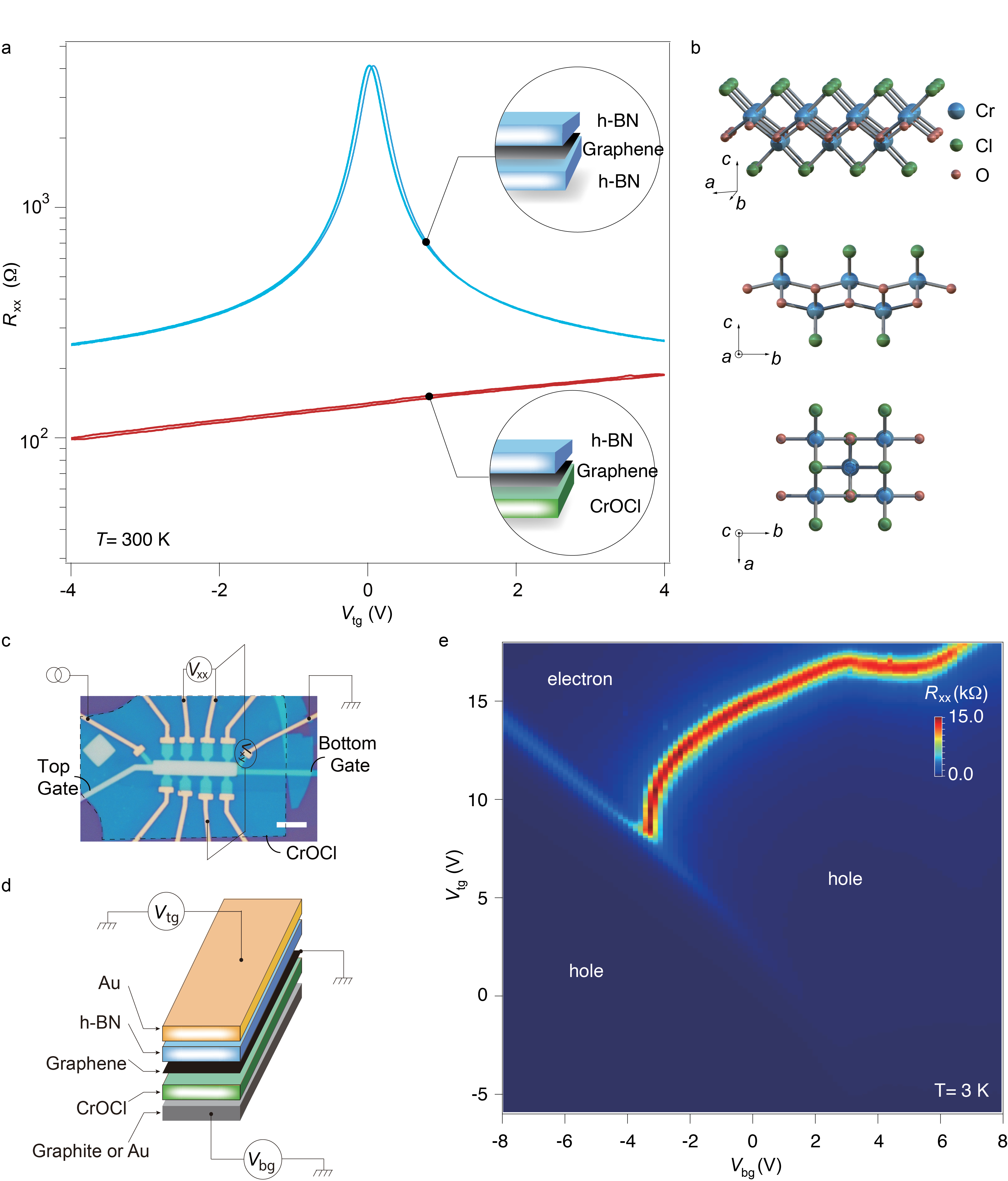
Characterizations of graphene/CrOCl heterostructures. Monolayered graphene as well as thin CrOCl flakes and encapsulating hexagonal boron nitride (h-BN) flakes were exfoliated from high-quality bulk crystals and stacked in ambient condition using the dry transfer method.[27] The vertically assembled van der Waals heterostructures were then patterned into Hall bars with their electrodes edge-contacted. As seen in Fig. 1a, the field-effect curve of h-BN/graphene/CrOCl samples (red curve) differs significantly with the conventional h-BN/graphene/h-BN ones (blue curve), with the resistive Dirac peak disappearing and the conductivity, in general, is enhanced compared with the former structure but with degraded gate tunability (art views of each configurations are illustrated in inset of Fig. 1a). Figure 1b shows the crystal structure of CrOCl, which consists of a Cr-O double-layer sandwiched between the Cl atom layers stacked along the -axis [28].
We first started with single gated devices and found that an SIC is taking place to affect the real doping in graphene that exhibits significant discrepancy from the doping expected from conventional gate dielectric, as shown in Supplementary Figures 1-6. Fig.1c shows the optical micrograph image of a typical h-BN/graphene/CrOCl heterostructure with top and bottom gates, with a cartoon illustrating the layered structure of such typical devices (Fig. 1d). An example of dual-gate mapping of resistance obtained at a temperature of =3 K is given in Fig.1e. Three notable regions are seen, each separated by a resistive peak and marked as either hole or electron doping, which is obtained via the analysis of the measurements at high magnetic fields, as will be discussed in the coming sections. To further elucidate the specific state of the SIC in the current hybrid system, we fabricated devices equipped with dual gates so that an effective displacement field can be applied to between the top and bottom gates, and at the same time the total carrier induced by the dielectrics from top and bottom gates can be tuned, as previously used in multiple-layered graphene devices [29, 30]. Here, and are the top and bottom gate capacitances per area, respectively. And and are the top and bottom gate voltages, respectively. and are residual doping and residual displacement field, respectively. Notice that the real doping in graphene that can be probed by transport measurement is affected by the interfacial states of CrOCl (see Supplementary Note 1), which can be different from in the interfacial coupling phase, as will be discussed in the coming text. Examples of plotting the dual gated map of channel resistance into the space of are given in Supplementary Figures 7-12.
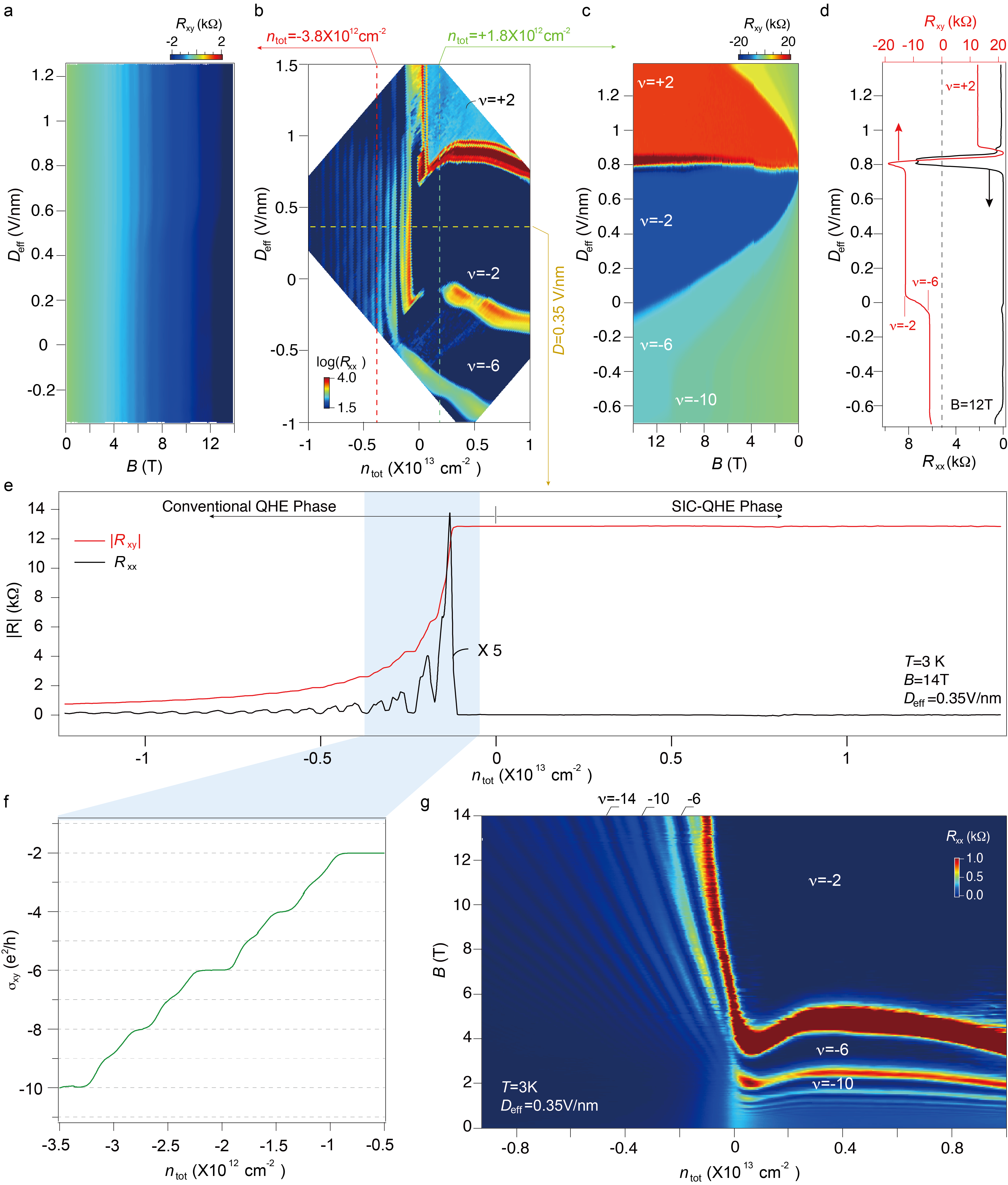
Gate tuned SIC in the quantum Hall regime. Figure 2a shows a magnetic field scan of along fixed carrier density at the hole side with (red dashed line in Fig. 2b, a mapping of channel resistance of Device-S16 in the space). Little -dependence of filling fraction (, LLs) is seen. This is a typical behavior of monolayer graphene, as there is no dimension and thus the displacement field does not affect the LLs in it. Strikingly, shown in Fig. 2c, magnetic field scan of transverse resistance along (green dashed line in Fig. 2b) exhibits drastically different patterns as compared to that in Fig. 2a. As discussed in the previous sections, with a single gate, only hole doping can be seen in graphene/CrOCl heterostructures (Supplementary Figure 4-5), and more details of carrier types in the dual gated devices can be found in Supplementary Figure 13. Here, at the fixed applied in Fig. 2c, dual gate sweep allows one to reach the electron side at 0.8 V/nm, as clearly indicated by the line profiles of both and at 12 T in Fig. 2d, where a well-developed quantum Hall plateau of can be seen. In this regime of and (we call it SIC-QHE phase), is quantized in an extremely wide parameter space. For example, at =14 T, filling fraction is found in the doping range of from 0 to 1013 cm-2, and a displacement difference of over 2 V/nm, which converts into a very large range of gate voltages. Notably, the quantized can be found in very low , reaching the zero magnetic field limit, which will be discussed in more details in the coming sections.
Fig. 2e shows the line profiles of and at a fixed displacement = 0.35 V/nm (along the yellow dashed line in Fig. 2b) at =14 T and =3 K. It is seen that on the hole side (noted as conventional QHE phase) in the curves, Landau quantizations are in agreement with that observed in conventional monolayered graphene [16, 15]. Fig.2f illustrates a zoomed-in view of transverse conductivity at between -0.5 1012 cm-2 and -3.5 1012 cm-2, indicating full degeneracy lifting with quantized plateaux at each integer filling fractions from =-2 to -10. This speaks the high mobility of the graphene in the conventional QHE phase in the graphene/CrOCl heterostructure. Indeed, by fitting of the hole-side part of effect curve at zero magnetic field (Supplementary Figure 14), hole carrier mobility is estimated to be about 104 cm2V-1s-1, which is comparable to the value in high-quality monolayer graphene reported elsewhere [27].
On the electron side of the line profiles of and in Fig. 2e, a SIC-QHE phase dominates, as the quantum Hall plateau of =-2 extends through out the whole gate range, up to +1.5 1013 cm-2. By varying the magnetic fields along fixed =0.35 V/nm, one obtains a color map in the parameter space of and , shown in Fig. 2g. It can be seen that the gate tunable SIC leads to a change of Landau quantization from the well-known fan-like behavior to a cascades-like one, as the system undergoes a phase transition from conventional QHE to SIC-QHE. To verify the as compared to in the sample in the low field limit ( 0.5 T before the quantum oscillation starts) in Fig. 2g, we extracted from Hall resistance at fixed (0.35 V/nm ), which shows a slope of 1 with at the conventional phase, but strongly departures at positive , as shown in Supplementary Figure 15. Moreover, to have a global picture of the major features described above, the color-maps shown in Fig.2 are re-plotted in a 3D presentation, as shown in Supplementary Figure 16. All these observations are reproducible in multiple samples (Supplementary Figure 17-18), and also confirmed in samples fabricated in a glove box, ruling out possible strong moisture or air adsorption in the interface of graphene/CrOCl heterostructures (Supplementary Figure 19).
Characteristics of the SIC-QHE phase. Central result of this letter is the observation of a SIC-QHE phase, where Landau quantizations seem to be “pinned” at a fixed filling fraction at a certain hole doping and at a fixed , such as shown in Fig. 2g. A trivial explanation for this would be that the coupling at the graphene-CrOCl interface has accumulated holes that screen and cancel out the positive gate voltages applied, leading to a failure of electron injection and thus the total effective doping remains pinned. However, the most striking feature in this work, as shown in Fig. 2b-c, is that the displacement field totally shuffles the Landau quantization (and hence the ), which rules out the “charge pinning” or “gate screening” picture, as the latter should be -independent just like in the conventional QHE phase (such as Fig. 2a). Moreover, the Landau quantization seems to be approaching the =0 limit in the SIC-QHE phase, as shown in Fig. 2c.
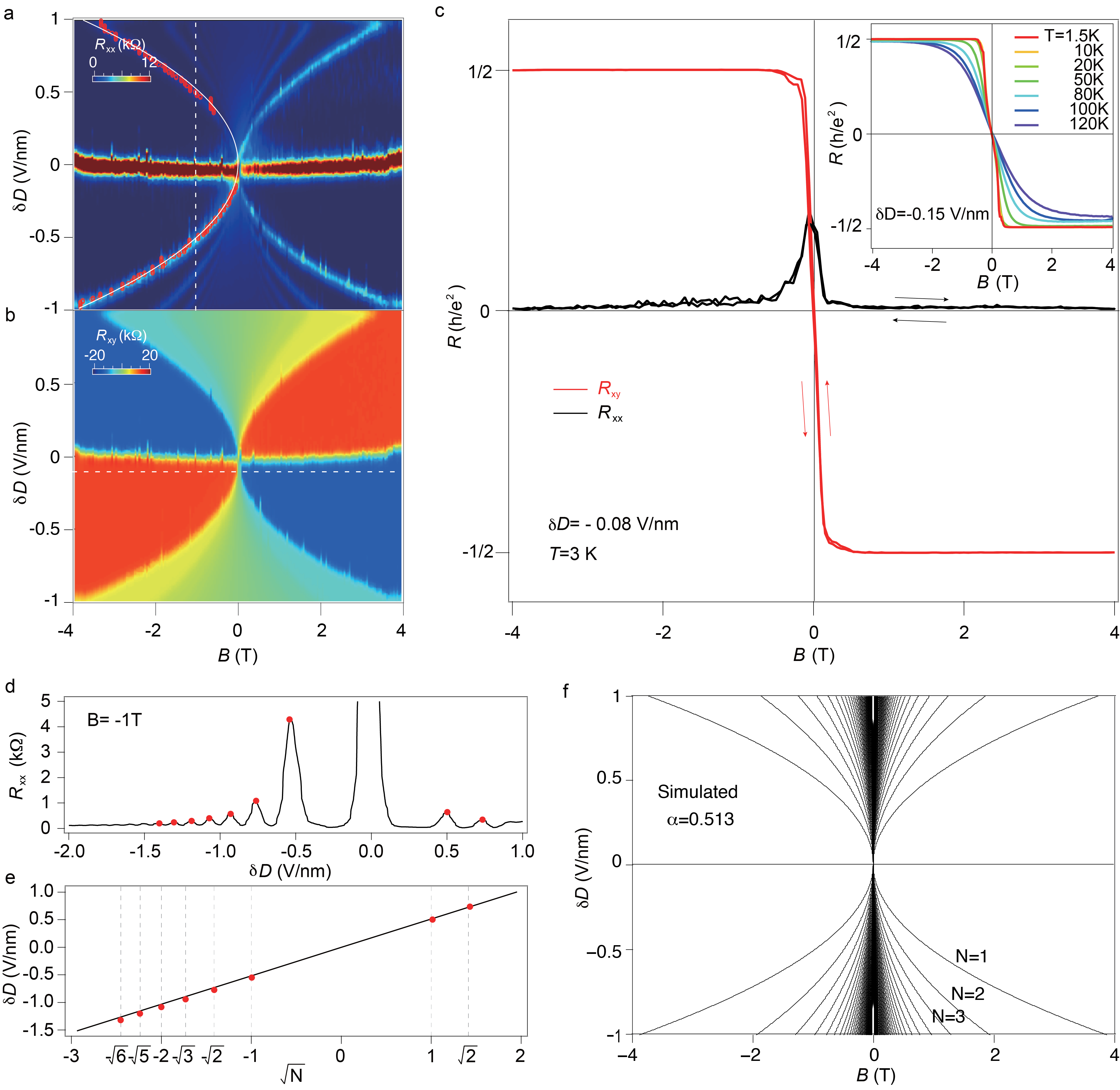
To further clarify this perplexing scenario, we carried out a zoomed-in scan of the low magnetic field part of Fig. 2c. We define the displacement field where carrier type switches from holes to electrons as , thus the axis can be renormalized as . As shown in Fig. 3a-b ( in Fig. 3a, and in Fig. 3b), was scanned in the range of -1 to +1 V/nm, while the magnetic field was scanned from -4 to +4 T. Wide Landau plateaux are seen in Fig. 3b, with the quantized regions indeed touching the =0 T line, while a tiny width still exists at the vicinity of zero magnetic field, due to the signal swap from positive to negative sign. The - relation of LLs observed here is distinct from those found in other multilayered graphene systems [31, 32, 33].
By bringing infinitely close to =0, one expects to have a Landau quantization at = 2 at the zero magnetic field limit. Due to experimental noises, we take the = -0.08 V/nm here (indicated by the white dashed line in Fig. 3b), and plotted both and in Fig. 3c. The curves indeed show well quantized plateaux at =0.5 starting from as low as sub 100 mT, with showing near zero reminiscent values at each plateau. Although quantum anomalous Hall effect (QAHE) or Chern insulator is claimed in suspended bilayer graphene and moir heterostructures such as aligned ABC-stacked trilayer graphene/h-BN,[34, 35, 36, 37] we found that our system of h-BN/monolayer-graphene/CrOCl heterostructure seems to be topologically trivial when magnetic field is completely absent, and the observed quantization at very low magnetic field is still in the regime of quantum Hall states, since the quantization of = is inherited from the Dirac electrons that are dominating in transport in the system, and no magnetic hysteresis (, the coercive field) is seen in the trace-retrace loop of magnetic scan in our system (indicated by red and black arrows in Fig.3c, and the zoomed-in scan in Supplementary Figure 20). More discussion can be seen in Supplementary Note 2. Trivial effect of gate leakage is ruled out, and multiple samples are tested to a maximum temperature before gate leakage takes place, shown in Supplementary Figure 21-23. Notably, this robust SIC-QHE phase in the graphene/CrOCl heterostructure prevails at much higher temperatures (inset of Fig. 3c) as compared to the QAHE systems so far reported, while the latter often requires temperatures of sub 2 K or even dilution fridge temperatures [35, 38, 39]. It also requires very relaxed experimental conditions as compared to such as doped (Hg,Mn)Te topological insulators quantum well, which is recently reported to show QH state below 50 mT at 20 mK [40]. It thus allows future applications in quantum metrology in the Systme International d’units [41, 13].
By extracting a line profile of in Fig. 3a at = -1 T (indicated by the vertical white dashed line), resistive peaks can be found at each LLs, as indicated by the red dots in Fig. 3d. It is found that the values at each resistive peak are in linear dependence with , with the LL, shown in Fig. 3e. This is a typical Landau quantization energy dependence in monolayered graphene. Indeed, - relation can be fitted using a parabolic curve as . Peaks of of the first LL in Fig.3a are picked as red circles, and fitted with a white solid parabolic curve, with =0.513. The first 200 LLs are then plotted in Fig. 3f, well simulating the experimental data. This indicates that linearly tunes the chemical potential of the Landau levels of graphene, which stimulates us to propose a possible mechanism in explaining the SIC-QHE to be explained in the following section.
Interestingly, the observed SIC-QHE phase seems to have no connection to the anti-ferromagnetic nature of CrOCl itself, as the Nel temperature of it is only 13 K, way lower than the upper bound temperature for the SIC-QHE phase. Recently, charge transfer phenomena have been also found in such as RuCl3/graphene systems, which give rise to a shifting of Raman signal or plasmonic characteristics in graphene, and seem to be often irrelevant to the magnetic order of the Cl-based substrates[42, 43]. Those other Cl-based compounds are reported to lead to inferior mobilities in the resulted hybrid systems, and are not suitable for QHE studies [25, 26]. In addition, we noticed that, a sister compound of CrOCl, FeOCl is far less stable, and could not be used to check the universality of the findings in this work (Supplementary Figure 24).
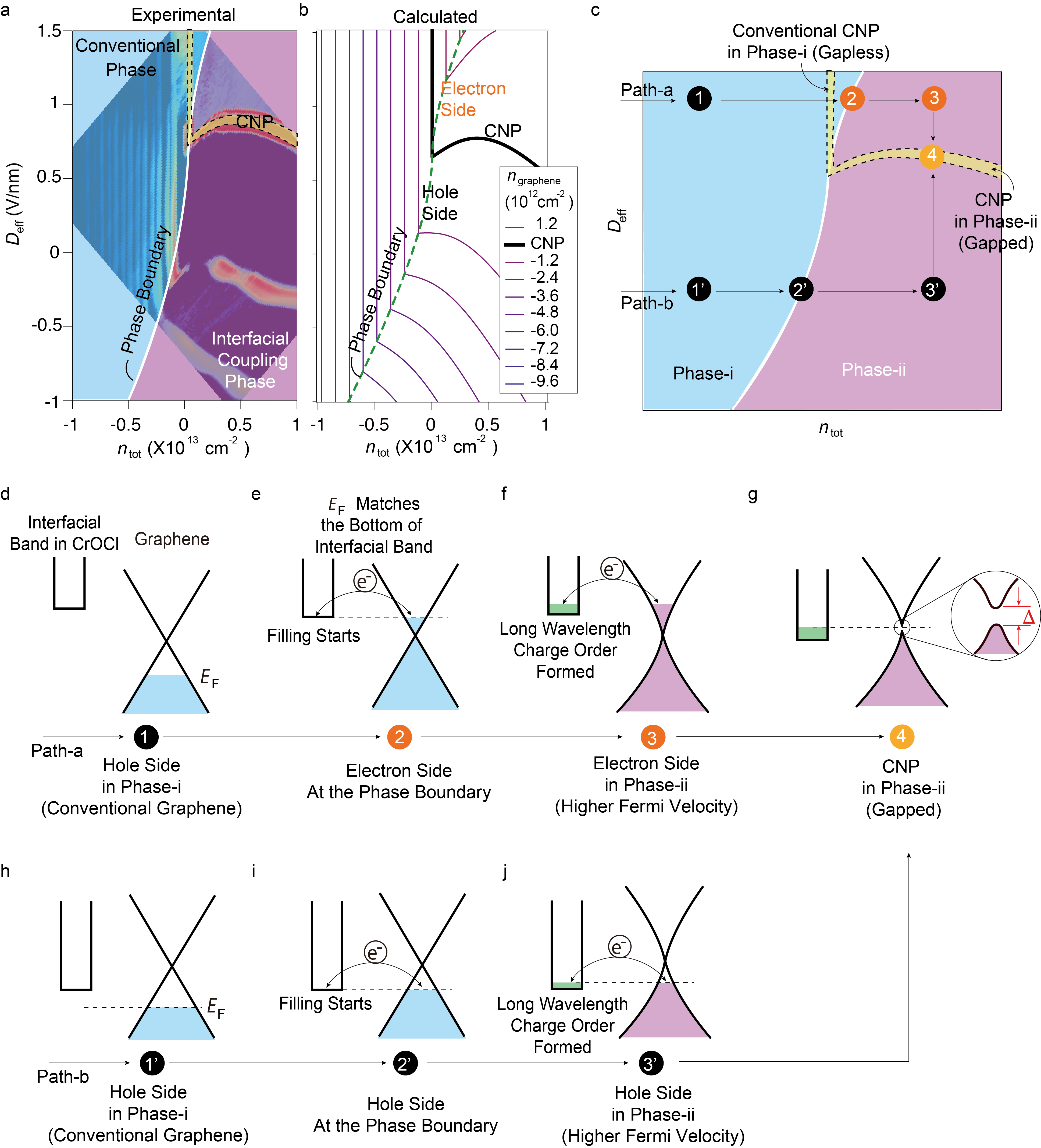
Possible mechanism of the SIC-QHE at zero field limit. We now replot in Fig. 4a the of Device-16 in the space at 12 T with falsed color that separates the boundary between the conventional and SIC phases. And the LLs naturally denote each iso-doping line associated to the fixed filling fraction , as defined by . Two key features are seen in Fig. 3a. First, the charge neutrality point (CNP) is bent as the system enters from conventional phase into the SIC-phase. Second, the spacing between each iso-doping lines increases as the system enters deeper into the SIC phase. To explain them, we propose an electro-static model in Supplementary Note 1. An interfacial band with considerable density of states near the CNP of graphene is introduced at the surface of CrOCl with a distance of below the graphene layer. While top and bottom gates are located at distances of and , respectively, as illustrated in Supplementary Figure 25a-b. By evaluating the model, we found that the above mentioned two major features can be well reproduced, as shown in the phase diagram in Fig. 3b. Nevertheless, one has to introduce in the simplified model two assumptions, including a band structure reconstruction with an enhanced Fermi velocity once the Fermi level of graphene touches the interfacial band, and also that the interfacial band exhibits no contribution to transport, as discussed in Supplementary Figures 25-28.
To elucidate the above simplified electro-static model, we performed DFT calculations considering systems with both monolayer and bilayer CrOCl supported graphene (Supplementary Figure 29-31 in Supplementary Note 2). It is seen that, in the bilayered CrOCl model and at certain vertical electric fields, the interfacial band from the top layer of CrOCl (mainly from the top Cr atoms, see Supplementary Figures 32-34) starts to overlap with the Dirac point of graphene, this is the event that charge transfer (i.e., filling of electrons in the interfacial band of CrOCl) from graphene to the interfacial band is triggered. Our DFT calculations suggest that long-wavelength localized charge order (Wigner crystal in our case, since the dimensionless Wigner-Seitz radii are estimated to exceed the critical value of 31 for 2D electrons,[44] shown in Supplementary Table 1) is formed in the interfacial band of Cr orbital in the top layer of CrOCl. It self-consistently explains that, once filled with electrons, the interfacial band undergoes Wigner instability and does not contribute to transport, but provides a superlattice of Coulomb potential for the graphene resting on top of CrOCl. When systematically considering the interplay between generic long-range Coulomb lattices and the Dirac electrons, our separate theoretical work suggests that such interaction in graphene indeed enhances the Fermi velocity dramatically and in the meantime opens a gap at the CNP.[45]
Based on the above analysis, we can then plot a schematic phase diagram in Fig. 3c, where the conventional and SIC phases are denoted as Phase-i and Phase-ii for simplicity. Two different paths are listed, to illustrate the doping processes of our system. In Path-a, graphene starts in a hole-doped conventional state (State-1 in Fig. 3d). It crosses the CNP, becomes electron-doped, and approaches the phase boundary where the Fermi level of graphene touches the lowest energy of the interfacial band in the top layer of CrOCl (State-2 in Fig. 3e), it thus triggers the electron-filling event (solid white phase boundary line in Fig. 3c) in the interfacial band. Upon entering in Phase-ii, the electrons filled in the interfacial band forms a Wigner crystal, which exerts a long-wavelength Coulomb potential to the Dirac electrons in graphene in such a way to renormalize the non-interacting band structures, thus interaction would play a more important role. Consequently, the Fermi velocity is significantly enhanced (sharpening of the Dirac cone in the illustration) driven by e-e interactions in graphene (State-3 in Fig. 3f). The system enters in Phase-ii, and remains electron-doped. Furthermore, when decreasing from State-3 to State-4, the Fermi level in graphene reaches its CNP, where an interaction-driven gap is seen (as supported by the extraction of thermal activation gap in Supplementary Figure 35). Upon further decreasing , the system becomes hole-doped again. Similar process can be interpreted for Path-a, in Fig. 3h-j.
Experimentally, by fitting the Shubnikov-de Haas oscillations from various temperatures at dopings in Phase-i and Phase-ii (Supplementary Figure 36), the cyclotron mass m∗ in Phase-i is estimated to be comparable to that in “ordinary” monolayer graphene, but 3-5 times larger than that in Phase-ii. It thus yields a few times higher Fermi velocity of graphene in Phase-ii, in agreement with the conjectures in our simplified electro-static model and DFT calculations. Thus in this regime the cyclotron gap of first LL will be in the order of about 100 meV at 0.1 T, which qualitatively explains the quantization at very low magnetic field. We emphasize that further probes such as infra-red transmission would be helpful in directly verifying the cyclotron gap estimated in the current system in this regard.
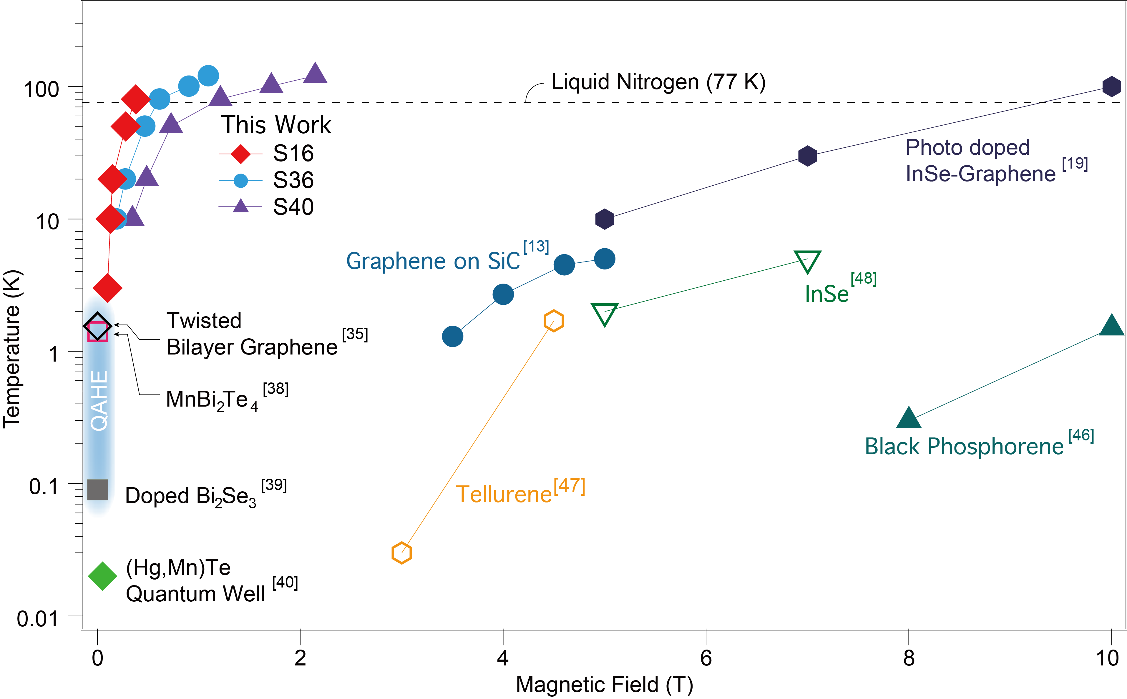
A robust quantum Hall state with ultra-low magnetic fields at relaxed experimental conditions can be crucial for future constructions of topological superconductivity as well as quantum information processing, which has long thought to be only possible in QAHE systems. It unambiguously tells that the interfacial coupling, in terms of engineering the quantum electronic states, is a powerful technique that we may have overlooked thus far. For comparison, Fig. 5 shows a diagram summarizing magnetic fields and temperatures required for realizing quantized Hall conductance in typical different QHE or QAHE systems [35, 38, 39, 40, 13, 19, 46, 47, 48], reported recently.
In conclusion, we have demonstrated a hybrid system of graphene/CrOCl, in which an exotic QHE phase was observed thanks to the peculiar gate tunable interfacial coupling. At finite magnetic fields and constant , a crossover from fan-like to cascades-like Landau quantization was seen. And in the - space, unlike the conventional -independent ones, LLs in the SIC-QHE phase exhibit parabolic dependence between and in a wide effective doping range from 0 to 1013 cm-2, with the Landau quantization of = plateau starting from as low as sub 100 mT below 10 K, and remains quantized at 350 mT at liquid nitrogen temperature. Our theoretical analysis self-consistently attribute the physical origin of this observed phenomenon to the formation of long wavelength charge order in the interfacial states in CrOCl and a band reconstruction in graphene subsequently. Our findings seem to open a new door of engineering the quantum Hall phase, and may shed light in the future manipulation of quantum electronic states via interfacial charge coupling, such as to construct novel topological superconductor, and to build quantum metrology standards.
I Methods
Sample fabrications and characterizations. The CrOCl/graphene/h-BN heterostructures were fabricated in ambient condition using the dry-transfer method, with the flakes exfoliated from high quality bulk crystals. CrOCl layers were etch patterned using an ion milling with Ar plasma, and dual gated samples are fabricated using standard e-beam lithography. A Bruker Dimension Icon atomic force microscope was used for thicknesses, morphology, and surface potential tests. The electrical performances of the devices were measured using a BlueFors LD250 at mK temperature, a Quantum Design PPMS system was used for temperature (3-300 K) and magnetic field (14 T) scannings, and a probe station (Cascade Microtech Inc. EPS150) for room temperature electrical tests.
Density functional theory calculations. Density functional theory calculations.The first principles calculations based on density functional theory (DFT) are carried out with Vienna Simulation Package (VASP) with projector augmented wave method [49, 50]. The plane-wave energy cutoffis set to be 600 eV, and the crystal structure is fully relaxed until the residual forces on atoms are less than 0.01 eV/. The generalized gradient approximation (GGA) by Perdew, Burke, and Ernzerhof is taken as the exchange–correlation potential [51]. Since Cr is a transition metal element with localized orbitals, the on-site Hubbard U = 2.7 eV parameter is used in the calculations. To properly include the effects of vertical electric fields, we focus on a bilayer CrOCl because monolayer is indifferent to electric fields. We have considered three magnetic configurations in the CrOCl, and the thickness of the vacuum region was set as 40 to avoid any artificial interactions. The“DFT+D2” type of vdW correction has been adopted for bulk calculations to properly describe the interlayer interactions [52, 53]. The so-calledfully localized limit of the spin-polarized GGA+U functional is adopted as suggested by Liechtenstein and coworkers [54, 55, 56, 57]. In the calculations of the commensurate supercell of bilayer-CrOCl/graphene heterostructure, a 24 supercell for bilayer CrOCl, and a 33 supercell for monolayer graphene have been adopted.
II DATA AVAILABILITY
The data that support the findings of this study will be available at the open-access repository Zenodo with a doi link, when published.
III Code AVAILABILITY
The codes used in theoretical simulations and calculations are available from the corresponding authors on reasonable request.
IV ACKNOWLEDGEMENT
This work is supported by the National Key RD Program of China (2019YFA0307800, 2017YFA0303400, 2018YFA0306900, 2020YFA0309601, and 2018YFA0306101), and is supported by the National Natural Science Foundation of China (NSFC) with Grants 11974357, U1932151, 52031014, 11974340, 12174257, and 51627801. This work is also supported by the Strategic Priority Research Program of the Chinese Academy of Sciences (Grant No. XDB28000000), the MOST of China (Grants No. 2018YFA0306101 and No. 2017YFA0303400), the Chinese Academy of Sciences (Grants No. QYZDJ-SSW-SYS001, and No. XDPB22). Growth of hexagonal boron nitride crystals was supported by the Elemental Strategy Initiative conducted by the MEXT, Japan ,Grant Number JPMXP0112101001, JSPS KAKENHI Grant Number JP20H00354 and A3 Foresight by JSPS.
V Author contributions
Z.H. and Y.Y. conceived the experiment. Z.H., Y.Y., J.Z., J.L. and Z.Z. supervised the overall project. X.L. and J.L. constructed the low-energy effective model. W.L., S.Z., J.L., J.K., K.C. performed the ab initio calculations. Y.G. performed the electro-static model. Y.W., X.G., K.Y., and N.R. carried out device fabrications, Y.W., X.G., K.Y., and P.G. performed electrical transport measurements; J.M. and Y.J. performed STM studies; K.W. and T.T. provided high quality h-BN bulk crystals. P.G. and Y.Y. carried out synthesis of CrOCl single crystals. Y.W., B.D., J.Z., J.M.,J.L., K.C., Y.Y., and Z.H. analysed the data. The manuscript was written by Z.H., J.L., and Y.W., with discussion and inputs from all authors.
VI ADDITIONAL INFORMATION
Competing interests: The authors declare no competing interests.
References
- [1] Amet, F. et al. Supercurrent in the quantum Hall regime. Science 352, 966 (2016).
- [2] Seredinski, A. et al. Quantum Hall-based superconducting interference device. Science Advances 5, eaaw8693 (2019).
- [3] Lindner, N. H., Berg, E., Refael, G. & Stern, A. Fractionalizing Majorana Fermions: Non-Abelian statistics on the edges of Abelian quantum Hall states. Phys. Rev. X 2, 041002 (2012).
- [4] Clarke, D. J., Alicea, J. & Shtengel, K. Exotic non-Abelian anyons from conventional fractional quantum Hall states. Nature Communications 4, 1348 (2013).
- [5] Mong, R. S. K. et al. Universal topological quantum computation from a superconductor-Abelian quantum Hall heterostructure. Phys. Rev. X 4, 011036 (2014).
- [6] Qiao, Z. et al. Quantum anomalous Hall effect in graphene proximity coupled to an antiferromagnetic insulator. Physics Review Letters 112, 116404 (2014).
- [7] Zhang, J., Zhao, B., Yao, Y. & Yang, Z. Quantum anomalous Hall effect in graphene-based heterostructure. Scientific Reports 5, 10629 (2015).
- [8] von Klitzing, K., Dorda, G. & Pepper, M. New method for high-accuracy determination of the finestructure constant based on quantized Hall resistance. Phys. Rev. Lett. 45, 494 (1980).
- [9] von Klitzing, K. Quantum Hall effect: Discovery and application. Annu. Rev. Condens. Matter Phys. 8, 13–30 (2017).
- [10] Klitzing, K. et al. 40 years of the quantum Hall effect. Nature Reviews Physics 2, 397–401 (2020).
- [11] Laughlin, R. B. Quantized Hall conductivity in two dimensions. Phys. Rev. B 23, 5632(R) (1981).
- [12] Avron, J. E., Osadchy, D. & Seiler, R. A topological look at the quantum Hall effect. Physics Today 56, 38 (2003).
- [13] Ribeiro-Palau, R. et al. Quantum hall resistance standard in graphene devices under relaxed experimental conditions. Nature Nanotechnology 10, 965–971 (2015).
- [14] Novoselov, K. S. et al. Room-temperature quantum Hall effect in graphene. Science 315, 1379 (2007).
- [15] Zhang, Y., Tan, Y. W., Stormer, H. L. & Kim, P. Experimental observation of the quantum hall effect and berry’s phase in graphene. Nature 438, 201–204 (2005).
- [16] Novoselov, K. S. et al. Two-dimensional gas of massless Dirac fermions in graphene. Nature 438, 197–200 (2005).
- [17] Amet, F. et al. Composite fermions and broken symmetries in graphene. Nature Communications 6, 5838 (2015).
- [18] Alexander-Webber, J. A. et al. Giant quantum hall plateaus generated by charge transfer in epitaxial graphene. Scientific Reports 6, 30296 (2016).
- [19] Bhuiyan, M. A. et al. Photoquantum hall effect and light‐induced charge transfer at the interface of graphene/inse heterostructures. Adv. Funct. Mater. 1805491 (2018).
- [20] Lara-Avila, S. et al. Non-volatile photochemical gating of an epitaxial graphene/polymer heterostructure. Adv. Mater. 23, 878–882 (2011).
- [21] Lartsev, A. et al. Tuning carrier density across Dirac point in epitaxial graphene on SiC by corona discharge. Appl. Phys. Lett. 105, 063106 (2014).
- [22] Berger, C. et al. Ultrathin epitaxial graphite: 2D electron gas properties and a route toward graphene-based nanoelectronics. J. Phys. Chem. B 108, 19912–19916 (2004).
- [23] Kudrynskyi, Z. R. et al. Giant quantum Hall plateau in graphene coupled to an InSe van der Waals crystal. Phys. Rev. Lett. 119, 157701 (2017).
- [24] Takenaka, H., Sandhoefner, S., Kovalev, A. A. & Tsymbal, E. Y. Magnetoelectric control of topological phases in graphene. Phys. Rev. B 100, 125156 (2019).
- [25] Zhou, B. et al. Evidence for charge transfer and proximate magnetism in graphene--RuCl3 heterostructures. Phys. Rev. B 100, 165426 (2019).
- [26] Mashhadi, S. et al. Spin-split band hybridization in graphene proximitized with -RuCl3 nanosheets. Nano Lett. 19, 4659–4665 (2019).
- [27] Wang, L. et al. One-dimensional electrical contact to a two-dimensional material. Science 342, 614–617 (2013).
- [28] Reuvekamp, P. Investigation into the magnetic and the structural properties of two low-dimensional antiferromagnets TiPO4 and CrOCl. Ph.D. Thesis, University of Stuttgart (2014).
- [29] Zhang, Y. et al. Direct observation of a widely tunable bandgap in bilayer graphene. Nature 459, 820–823 (2009).
- [30] Maher, P. et al. Tunable fractional quantum hall phases in bilayer graphene. Science 345, 61–64 (2014).
- [31] Weitz, R. T., Allen, M. T., Feldman, B. E., Martin, J. & Yacoby, A. Broken-symmetry states in doubly gated suspended bilayer graphene. Science 330, 812 (2010).
- [32] Sanchez-Yamagishi, J. D. et al. Quantum Hall effect, screening, and layer-polarized insulating states in twisted bilayer graphene. Phys. Rev. Lett. 108, 076601 (2012).
- [33] Stepanov, P. et al. Quantum parity Hall effect in Bernal-stacked trilayer graphene. Proc. Natl. Acad. Sci. U.S.A. 116, 10286–10290 (2019).
- [34] Geisenhof, F. R. et al. Quantum anomalous hall octet driven by orbital magnetism in bilayer graphene. Nature 598, 53–58 (2021).
- [35] Serlin, M. et al. Intrinsic quantized anomalous hall effect in a moir heterostructure. Science 367, 900 (2020).
- [36] Chen, G. et al. Tunable correlated chern insulator and ferromagnetism in a moir superlattice. Nature 579, 56 (2020).
- [37] Li, T. et al. Quantum anomalous hall effect from intertwined moir bands. Nature 600, 641–646 (2021).
- [38] Deng, Y. et al. Quantum anomalous Hall effect in intrinsic magnetic topological insulator MnBi2Te4. Science 367, 895–900 (2020).
- [39] Chang, C. Z. et al. Experimental observation of the quantum anomalous Hall effect in a magnetic topological insulator. Science 340, 167 (2013).
- [40] Shamim, S. et al. Emergent quantum hall effects below 50 mT in a two-dimensional topological insulator. Science Advances 6, eaba4625 (2020).
- [41] Lafont, F. et al. Quantum hall resistance standards from graphene grown by chemical vapour deposition on silicon carbide. Nature Communications 6, 6806 (2015).
- [42] Wang, Y. et al. Modulation doping via a two-dimensional atomic crystalline acceptor. Nano Letters 20, 8446–8452 (2020).
- [43] Rizzo, D. J. et al. Charge-transfer plasmon polaritons at graphene/-RuCl3 interfaces. Nano Letters 20, 8438–8445 (2020).
- [44] Tanatar, B. & Ceperley, D. Ground state of the two-dimensional electron gas. Phys. Rev. B. 39, 5005 (1989).
- [45] Xin Lu, X., Shihao Zhang, S., Zheng Vitto Han, Z. & Jianpeng Liu, J. Synergistic interplay between Dirac fermions and long-wavelength order parameters in graphene-insulator heterostructures. arXiv:2206.05659 (2022).
- [46] Li, L. et al. Quantum Hall effect in black phosphorus two-dimensional electron system. Nature Nanotechnology 11, 593 (2016).
- [47] Qiu, Q. et al. Quantum Hall effect of Weyl fermions in n-type semiconducting tellurene. Nature Nanotechnology 15, 585 (2020).
- [48] Bandurin, D. A. et al. High electron mobility, quantum Hall effect and anomalous optical response in atomically thin InSe. Nature Nanotechnology 12, 223 (2017).
- [49] Kresse, J. & Furthmler, J. Efficient iterative schemes for total-energy calculations using a plane-wave basis set. Phys. Rev. B 54, 11169 (1996).
- [50] Kresse, J. & Furthmler, J. Efficiency of total energy calculations for metals and semiconductors using a plane-wave basis set. Comput. Mater. Sci. 6, 15 (1996).
- [51] Perdew, J. P., Burke, K. & Ernzerhof, M. Generalized gradient approximation made simple. Phys. Rev. Lett. 77, 3865 (1996).
- [52] Grimme, S. Semiempirical GGA-type density functional constructed with a long-range dispersion correction. J. Comput. Chem. 27, 1787 (2006).
- [53] Buko, T., Hafner, J., Lebgue, S. & ngyn, J. G. Improved description of the structure of molecular and layered crystals: Ab initio DFT calculations with van der Waals corrections. J. Comput. Chem. 114, 11814 (2010).
- [54] Liechtenstein, V. I., A. I. adnd Anisimov & Zaanen, J. Density-functional theory and strong interactions: Orbital ordering in Mott-Hubbard insulators. Phys. Rev. B 52, R5467 (1995).
- [55] Czyyk, M. T. & Sawatzky, G. A. Local-density functional and on-site correlations: The electronic structure of La2CuO4 and LaCuO3. Phys. Rev. B 49, 14211 (1994).
- [56] Anisimov, V. I., Solovyev, I. V., Korotin, M. A., Czyyk, M. T. & Sawatzky, G. A. Density-functional theory and NiO photoemission spectra. Phys. Rev. B 48, 16929 (1993).
- [57] Solovyev, I. V., Dederichs, P. H. & Anisimov, V. I. Corrected atomic limit in the local-density approximation and the electronic structure of impurities in Rb. Phys. Rev. B 50, 16861 (1994).