Anatomy of nanomagnetic switching at a 3D Topological Insulator PN junction
Abstract
A P-N junction engineered within a Dirac cone system acts as a gate tunable angular filter based on Klein tunneling. For a 3D topological insulator with a substantial bandgap, such a filter can produce a charge-to-spin conversion due to the dual effects of spin-momentum locking and momentum filtering. We analyze how spins filtered at an in-plane topological insulator PN junction (TIPNJ) interact with a nanomagnet, and argue that the intrinsic charge-to-spin conversion does not translate to an external gain if the nanomagnet also acts as the source contact. Regardless of the nanomagnet’s position, the spin torque generated on the TIPNJ is limited by its surface current density, which in turn is limited by the bulk bandgap. Using quantum kinetic models, we calculated the spatially varying spin potential and quantified the localization of the current versus the applied bias. Additionally, with the magnetodynamic simulation of a soft magnet, we show that the PN junction can offer a critical gate tunability in the switching probability of the nanomagnet, with potential applications in probabilistic neuromorphic computing.
pacs:
Valid PACS appear hereThree-dimensional topological insulator surfaces enjoy gapless topological surface states (TSS) protected by spatial inversion and time-reversal symmetry. In many ways, they are similar to low-energy graphene bands, except the Dirac cones are labeled by spins rather than pseudospins, with a similar Chern number chen2009experimental ; xia2009observation ; zhang2009topological . Numerous novel physical phenomena have been explored with TSS across graphene PN junctions. In particular, we can draw inspiration from graphene PN junctions that have served as a convenient laboratory for Klein tunnel devices, with potentially important contributions to low-power digital as well as high-speed analog switches beenakker2008colloquium ; stander2009evidence ; sajjad2013manipulating ; reza_modeling_2016 ; chiba_magnetic-proximity-induced_2017 ; fert_efficiency ; SOT3dTI .
The intrinsic spin-momentum locking of TSS in a TI material allows conversion of a charge current into a spin current at a higher efficiency than heavy metal underlayers in common spin-orbit torque devices Fan2014 ; PRLSOT ; SOTfert . In fact, the spin-momentum locking feature of TSS imposes spin conservation rules across a PN junction, suggesting a charge-to-spin conversion ratio (scaled dimensionally like the Spin Hall Angle except between longitudinal current densities) can exceed unity and be as high as 20 habib2015chiral . This number is much higher than the Spin Hall Angle measured in heavy metals such as Pt ()liu2011spin , -Ta ()liu2012spin , and in Pt-doped Au ()gu2010surface . However, besides an idealized assumption about the presence of a large non-leaky bandgap (perhaps more suitable to TIs like SmB6 than Bi2Se3), it is also worth emphasizing that the spin ‘amplification’ effect was studied on a homogeneous TIPNJ, where the source/drain contacts are assumed to be extensions of the TI surface as well. While it is easy to over-generalize the high charge-to-spin conversion efficiency to the TI-ferromagnet interface, it is not a straightforward equivalence to the homogeneous TI surface and deserves proper analysis.
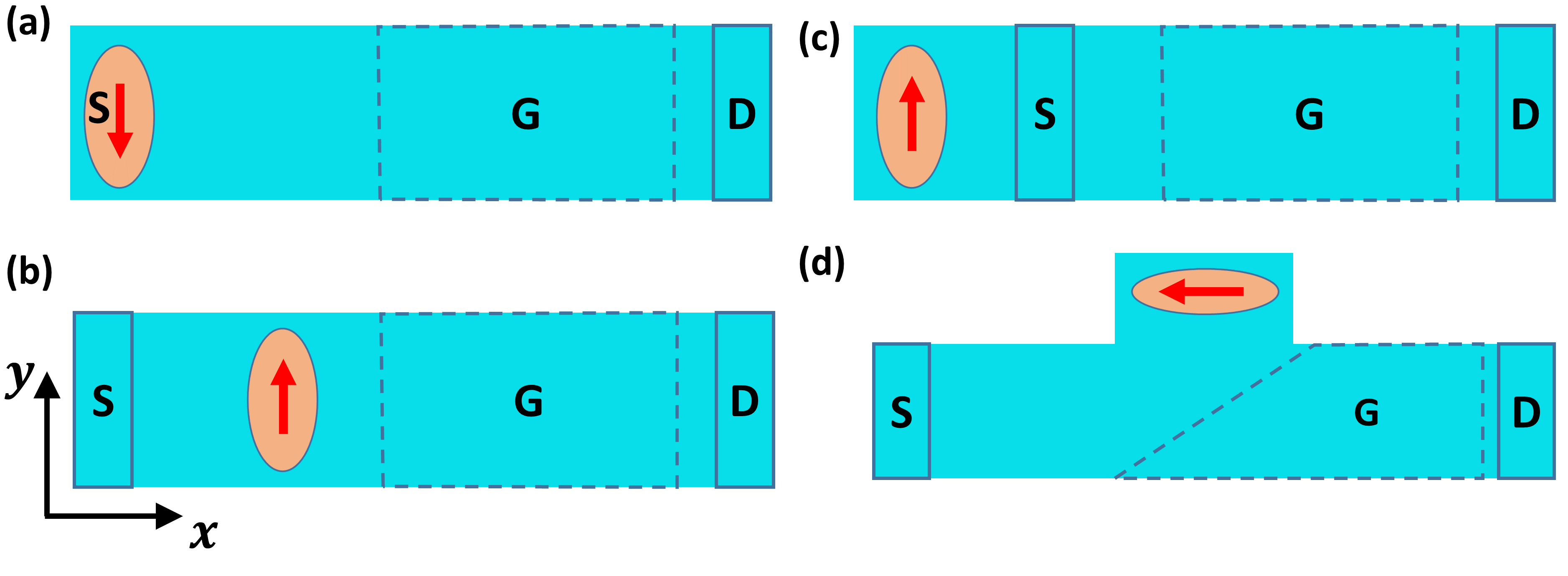
In this paper, we argue that the aforementioned large spin amplification is an intrinsic effect that does not automatically induce a large spin current across the TI/nanomagnetic contact interface. Fig. 1 shows some possible setups for a nanomagnet on TIPNJ. Our focus is on configuration (a) and we will use Non-Equilibrium Green’s Function (NEGF) simulations on the TSS to help clarify the difference between intrinsic versus extrinsic charge-to-spin gain in TIPNJ. We also show a NEGF treatment of a full 3D slab that allows us to compare the surface versus bulk shunt resistances. In practice, it can be a challenge to isolate the surface contribution from the bulk in common binary TI compounds such as , taskin2009quantum ; butch2010strong . One possible solution is to alloy the binary TIs into ternary compounds like tuned to have a low carrier density in the bulk jia2011low . Another way to improve the TSS portion of the total current is by inserting a ferromagnetic layer with a perpendicular anisotropy to one surface (Fig 5.b,c), which we will cover later.
A PN junction provides a gate tunable filter on the spins. For sufficient current densities it can flip a low barrier in-plane magnet unidirectionally. The latter can be flipped back with an oppositely directed current in a symmetric set-up. The low barrier magnet is useful for three-terminal stochastic computing ASN ; BSN , where the PN junction provides a gate tunability of the average magnetization that follows a neuron-like nonlinear activation function.
Computational Method. Near the Dirac point, the 3DTI Hamiltonian can be described as zhang2009topological :
| (1) |
with , and . For , the parameters used are: . These parameters yield a bulk bandgap of . We used the 3D Hamiltonian to study the surface versus bulk current. By discretizing the 3DTI Hamiltonian we get the lattice Hamiltonian:
| (2) |
Where , , , and H.C. is the Hermitian conjugate. The z-direction is set perpendicular to the quantum layers. While the 3DTI Hamiltonian was used to study the bulk-surface current distributions and current shunting, we need to adopt a simpler TSS model for simulating the charge/spin transport in the combined system of a TIPNJ and a nanomagnet (Fig. 2): . To discretize this Hamiltonian, a Wilson mass term needs to be added to avoid the fermion doubling problem hong2012modeling :
| (3) |
where , , . is the grid spacing, , and is a fitting parameter set to to generate a bandstructure that reproduces the ideal linear bands within a energy window of habib2015chiral . is the normal vector to the surface and is the speed of electrons near the Dirac point. are the Pauli matrices.
A generic ferromagnetic (FM) nanomagnet is modeled by a tight-binding Hamiltonian in a cubic lattice with a single orbital per site:
| (4) |
where is the onsite energy. is the exchange energy split along the direction of the magnetization . goes through all neighbors of site . is the electron hopping energy with effective electron mass . The hopping term between the FM and TI surface is tuned to to minimize the contact resistance. The FM parameters result in a spin polarization around the Fermi energy with density of states for the spin up ()/down () channels. These numbers are a bit lower than the nanomagnet modeled in roy2015magnetization , mostly due to the reduced size of our simulated magnet. Fig. 2 shows the discretization of the coupled system including the ferromagnetic contact and the TI surface. The TI surface is assumed to be doped N-type with a single gate controlling the drain side. The periodic boundary condition is adopted in the direction and characterized by the transverse quasi-momentum .
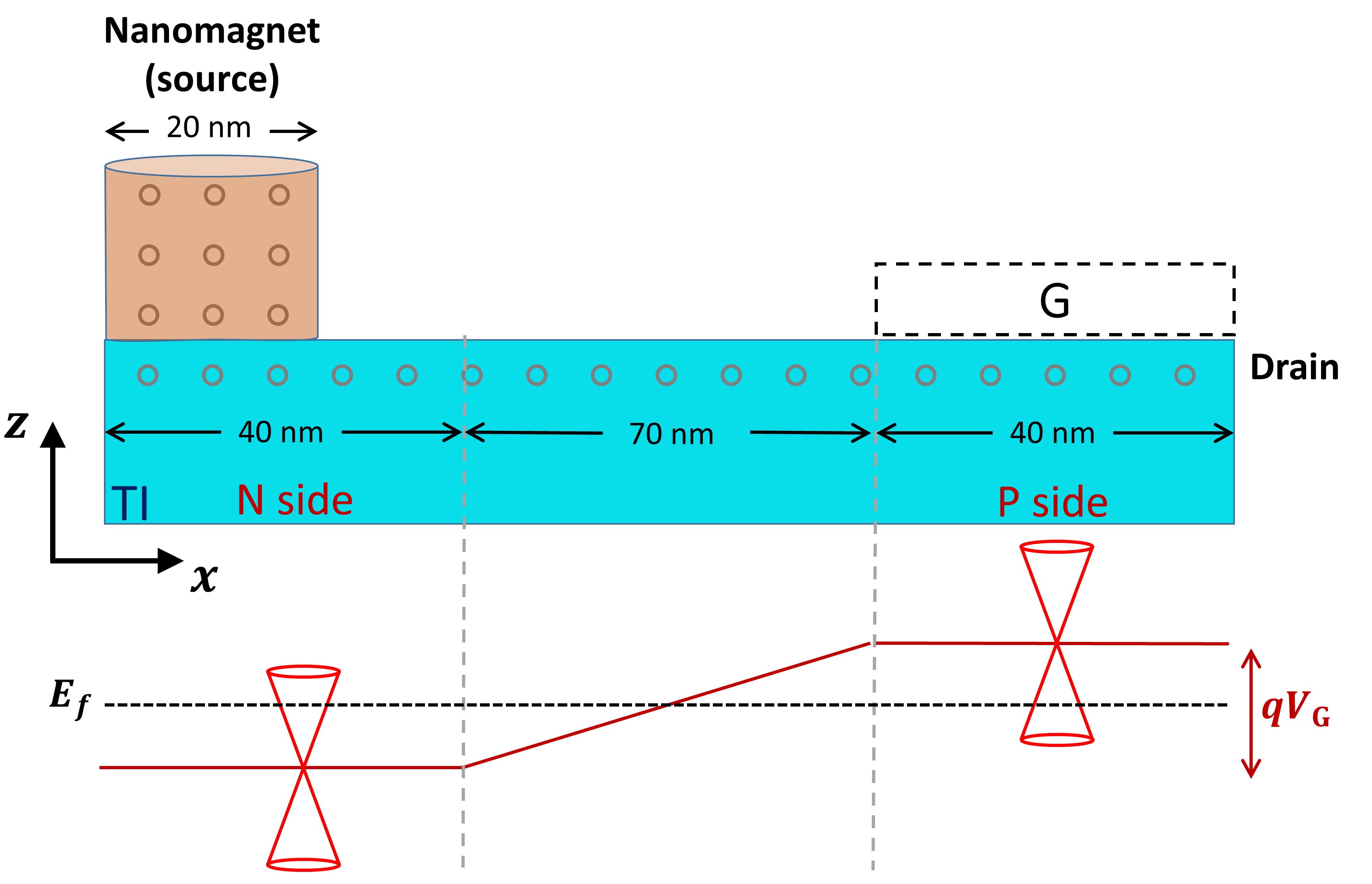
Part of the FM contact is included in the channel Hamiltonian while the rest is assumed to be infinite in the +z direction and modeled by a self-energy using recursive Green’s functions. For simplicity, the drain is just an extended part of the TI surface and included as a surface self-energy term that can be obtained with an iterative approach sancho1985highly . The retarded Green’s function and electron correlation matrix can be calculated through the Non-Equilibrium Green’s function method datta1997electronic
| (5) | |||||
| (6) |
with the Fermi-Dirac distribution function on the source/drain sides, and the identity matrix. The charge current is conserved throughout the structure and can be evaluated as:
| (7) |
while the charge and spin current from site to are calculated as:
| (8) |
The bias induced carrier density where are obtained from:
| (9) |
where is the equilibrium Fermi-Dirac distribution.
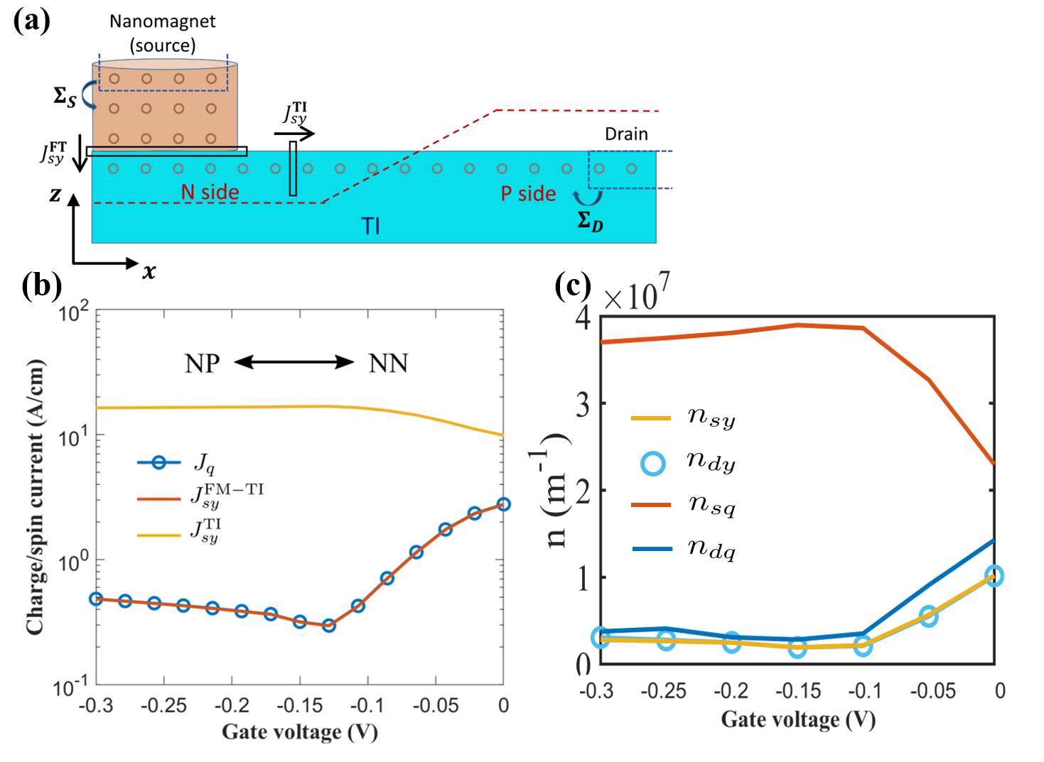
Results: charge-to-spin conversion in TIPNJ. Our previous workhabib2015chiral showed that the TIPNJ acts like a spin collimator that increases the non-equilibrium spin current while reducing the charge current at the same time. The corresponding spin-to-charge ratio (the longitudinal equivalent of the Spin Hall Angle ) at the source contact can go up to as high as habib2015chiral . While it is easy to assume that this conversion would dramatically improve the switching efficiency if we replace the ‘TI source contact’ with a ferromagnetic contact, we show here that the impressive gain is limited to the TI surface (we refer to this as the ‘intrinsic’ gain). To see the difference between the intrinsic and the external gain, we calculated the spin current at two locations along the transport direction: one between the FM contact and the TI surface, the other one on the N-type TI surface, as indicated in Fig. 3(a). Fig. 3(b) compares the charge current with the spin currents at the above-mentioned locations as a function of the gate voltage. As the gate voltage sweeps from to , the TI surface transitions from a PN junction to a homogeneous N-type surface. The behavior of the charge current (independent of where it is being calculated) and TI surface spin current , with a maximum ratio of resembles the results from habib2015chiral , where the PN junction effectively suppresses the charge current while amplifying the nonequilibrium spin current. However, the spin current across the nanomagnetic contact does not follow the in-plane surface spin current but instead follows the charge current. While the ratio is very close to , never exceeds the charge current regardless of which regime the TI surface is in. Looking at the bias-induced charge and spin carrier density, we can see the picture more clearly (Fig. 3.c). The spin density shows no change on the source and drain sides of TI. However, the charge densities show significant variations in the source and drain regions (opposite of currents’ behavior). This further solidifies the above explanation, as the charge densities from the incoming and reflected currents add up in the source region but are subtracted for spin density.
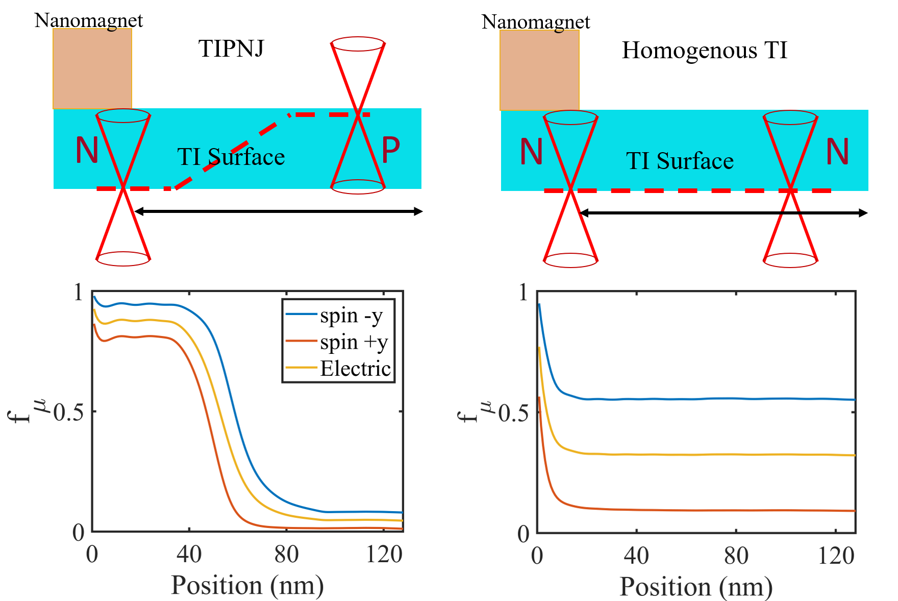
To better understand this discrepancy, we look at the individual Fermi levels in each spin channel (where spin-up corresponds to while spin-down corresponds to ) on the TI surface (Fig. 4). The Fermi levels are calculated by simulating a magnetic probe at each lattice point which draws net zero currents from the channel with negligible deformation of the channel Hamiltonian. The calculated quantity is hong2012modeling where is the coupling between FM probe and the TI surface with being the coupling strength. Due to the spin-momentum locking of the TI surface states, electrons in the spin-up channel can only move in the direction while electrons in the spin-down channel move in the opposite direction, roughly along two one-way streets (for 3D TSS, the angular transition is continuous)yunkunklein . This behavior results in the ‘intrinsic’ spin amplification observed on the TI surface: non-equilibrium electrons moving in opposite directions due to electron reflection at the PN junction reduce the net charge current while increasing the net nonequilibrium spin current. However, when the nanomagnet contact exchanges electrons with the TI surface, the electrons flow bidirectionally regardless of their spin orientations. Ultimately, the rate of influx and outflow of spins from the nanomagnet is controlled by the difference in the electrochemical potentials between the magnet and the TI surface. Being the source contact, the magnet has the highest electrochemical potential in both spin channels. Therefore one expects a net outflow of electrons from the magnet to the TI surface in both spin channels. The net spin current is just the difference between the charge currents in different spin channels, which is always lower than the sum of them. The extrinsic spin amplification in this configuration, with the magnet doubling as the current source, cannot exceed unity.
The limit on external charge-to-spin gain is imposed by having the nanomaget as the source contact. A more common setup is to have a floating nanomagnet on top of a TI (see fig. 1(b)). There are several research papers that discuss this configuration (without a PN junction) in detail, such as the proximity effect induced by the magnetic field from the magnet duan2015nonlinear , and the shunting of the charge current from the TI surface to a conductive magnetic layer roy2015magnetization . With this configuration, the electrochemical potential of the nanomagnet is free to adjust in order to draw a net zero charge current.
The charge-to-spin conversion rate depends on the splitting of the electrochemical potentials of the opposite spin channels. With TIPNJ, Fig. 4 shows that the splitting narrows compared to the homogeneous TI surface, which means the PN junction effectively turns off the spin torque from the TI surface.
.
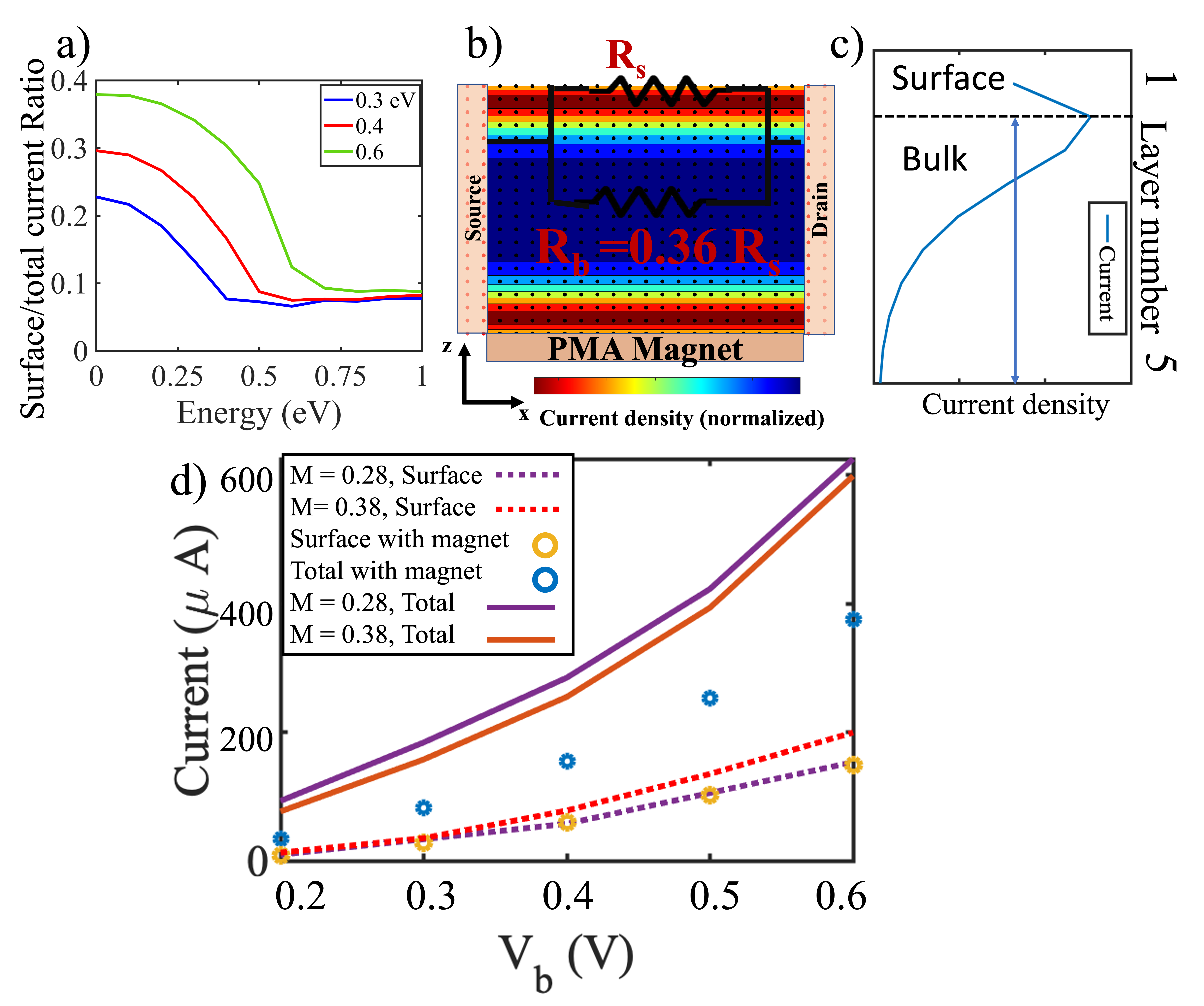
Because of the current shunting to the bulk of the 3DTI, the surface spin current calculated from TSS Hamiltonian Eq. 3 is overestimated. To study the surface-bulk current distribution, the 3DTI Hamiltonian as described in Eq. 2 is employed. With equation 8, the current density for each layer is calculated and separated into bulk and surface currents. To get a simple resistance model, we use two parallel resistances for bulk and surface . Based on the current distributions, the ratio of resistances is calculated. Here we define the surface current as the current in the top (bottom) layers: starting from the top (bottom) surface layer to the layer where the current density is peaked as shown in Fig. 5.c. TSS has a practical limitation on how much current increases with applied bias. For electrons with higher energies that are only accessible with a higher bias, the conductive state will no longer be strongly localized at the surface and will shunt into the bulk (Fig. 5(a)). Such a shunting 3dTIacoustic implies that a significant portion of the current will be diverted away from the surface, reducing the carrier exchange between the FM and TI and degrading the switching efficiency. Increasing the bias above the bulk bandgap will therefore have diminishing returns. For example, for the localized current at the surface (about thick, Fig. 5.b) carries only of the total current. One way to alleviate this is by finding a 3DTI material with a larger bulk bandgap, as can be seen in Fig 5(a-b). Alternatively, inserting or doping the TI surface in contact with the substrate (Fig. 5b,d) the 3DTI grown on with a PMA magnet can also increase . This is due to the fact that out-of-plane Zeeman energy kane ; nikolic3dti ; chiba_magnetic-proximity-induced_2017 ; tokura_magnetic_2019 (Added as to TI onsite energy for the bottom surface) opens up a gap. Since this effect is localized only at one surface, the opposite surface is nearly unaffected. However, the total current is now smaller as the total resistance of the channel is increased.
TIPNJ as a RAM. For the nanomagnet-as-source-contact configuration sans external gain, the gate controls the TIPNJ resistance and thus can be used to tune the total spin current and the spin torque applied on the nanomagnet. The structure of such a device is shown in Fig. 6, where the TIPNJ would have a transistor-like behavior. However, the maximum bias window is limited by the bandgap of the bulk TI. While we have discussed ways to alleviate the shunting issue, they might be challenging to achieve experimentally. Having said that, we looked at a possible 1 transistor-1 magnetic tunnel junction (1T1MTJ) 1T1MTJ device based on TIPNJ. The switching of a magnet parallel or anti-parallel to the injected spin current polarization is known as the anti-damping switching. The required critical spin current is given by (ignoring the effects of the rotation of spins from interfacial Zeeman field) sun :
| (10) |
where is the dimensionless energy barrier and is the Gilbert damping. From NEGF calculations, we can see that at low biases, spin currents of at a width of 40 is achievable. This would be enough to switch a magnet with (needed for a reliable memory at room temperature liu2012spin ), at a write error rate (WER) of and a switching time of . The switching roughly translates to an energy consumption of . It has been reported that 3DTI can be more energy efficient than heavy metals PRLSOT ; Liu_ti . However, by improving the interfacial quality of FM and heavy metal, a significant increase in efficiency of heavy metal has also been reported fert_efficiency ; improvedHM . This suggests that although 3DTI might not provide higher energy efficiency compared to heavy metals, TIPNJ can operate at low voltages suitable for more energy efficient applications such as RAM. For instance, the tuning of the TI surface state can be achieved by small applied voltages ( as compared to for CMOS transistors).
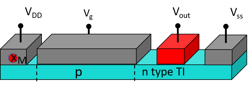
From a practical perspective, the required on/off current ratio from reliable spin torque switching can be deducted from the error rate butler ; fokker :
| (11) |
For a typical write error rate , the minimum is about 5.5. In comparison, the calculated from NEGF simulations shows that the gating mechanism works well enough for a TI based 1T-1MTJ RAM.
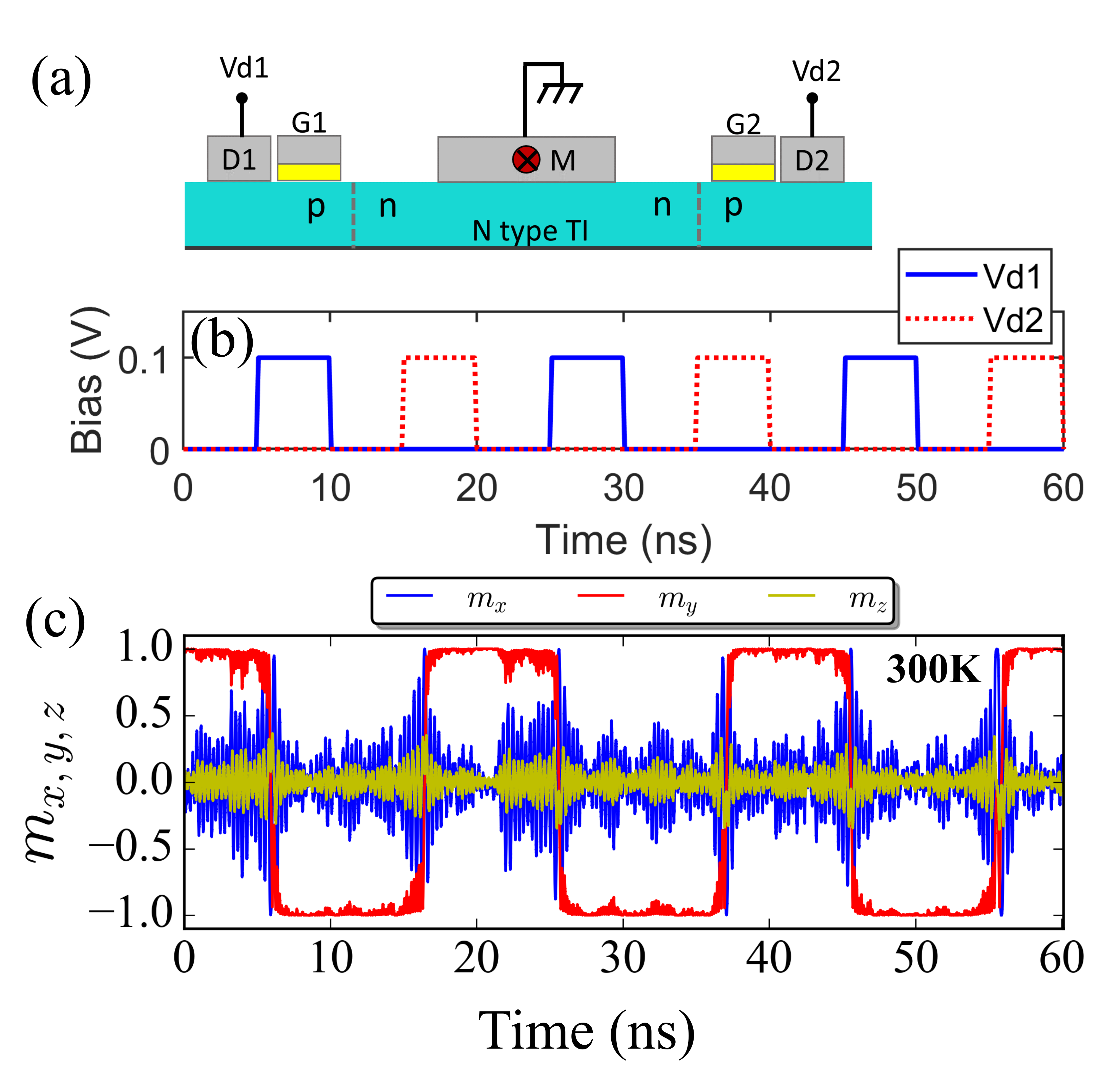
Volatile Memory. Although it is possible to enhance the TIPNJ current through material engineering to achieve the required current to drive traditional RAM applications, we also explored what is possible under conditions where leakage current and interfacial imperfections lower the spin current generated on a TIPNJ. To quantify the driveability of the TIPNJ, we have simulated the magnetodynamics of a nanomagnet under the TIPNJ current with the phenomenological Landau-Lifshitz-Gilbert (LLG) equation with a stochastic Langevin correction:
| (12) |
where is the normalized magnetic moment; is the effective field from the intrinsic anisotropy of the magnet; is the saturation magnetization; is the volume of nanomagnet; is the spin current with the vector pointing at the spin direction. is a stochastic thermal torque term representing the thermal noise. a three dimensional Gaussian white noise with mean and standard deviation of . First, we propose a configuration (Fig. 7(a)) for an experimental verification of the switching of a nanomagnet from a TIPNJ. A symmetric structure is needed for flipping the magnetization back-and-forth, generating a periodic signal that can be read out by stacking an MTJ or spin valve structure on top of the switching magnet. Our simulation shows that the TIPNJ can reliably drive a small magnet with an adequate anisotropy energy barrier () to reliably switch back and forth with a current (proportional to the longitudinal dimension of the magnet) as low as . When we further lower the anisotropy barrier, we entered a regime where the tunability of the TIPNJ is favored over its driveability. A nanomagnet with very small energy barrier () can operate in the stochastic switching regime. At room temperature, those magnets flip their magnetic moments frequently and stochastically under the influence of thermal noise. A small current can tip the balance of the two energy minimum orientations along the easy axis and affect the probability of the magnetic moment pointing at the direction decided by the current direction, with a binary stochastic neuron like tanh behavior on average. Fig. 8 shows the tuning of switching probability under a small spin current generated from the TIPNJ. The state (probability) of the nanomagnet can be extracted through a time-average measurement on the magnetic moment. This kind of setup can be used in generating random numbers fukushima2014spin , or stochastic signal processing ganguly2018analog . The energy cost for this is calculated to be .

Conclusion. In this paper, we have taken a closer look at the tuning of the TSS spin current in a TIPNJ as was originally proposed in habib2015chiral . We have analyzed the intricate nature of the charge-to-spin conversion on the TI surface with a nanomagnetic source contact. More importantly, we have clarified an important difference between the intrinsic charge-to-spin gain observed on a homogeneous TI surface, and the external gain useful for switching a nanomagnet. Additionally, we have looked at the limitations on the magnitude of the surface current, which is mostly determined by the bulk bandgap, and discussed two ways to improve it. While those issues seem to suggest the TIPNJ might not be able to offer a superior solution for common memory/logic applications, it can still work well as a RAM because of its gate tunability and low bias operation. Furthermore, the spatial programmability introduced by the PN junction may find use in novel applications such as probabilistic or neuromorphic applications.
Acknowledgments. This work is supported by the Army Research Lab (ARL) and in part by the NSF I/UCRC on Multi-functional Integrated System Technology (MIST) Center; IIP-1439644, IIP-1439680, IIP-1738752, IIP-1939009, IIP-1939050, and IIP-1939012. We acknowledge helpful discussions with Mahesh Neupane and George De Coster at ARL.
References
- [1] YL Chen, James G Analytis, J-H Chu, ZK Liu, S-K Mo, Xiao-Liang Qi, HJ Zhang, DH Lu, Xi Dai, Zhong Fang, et al. Experimental realization of a three-dimensional topological insulator, bi2te3. science, 325(5937):178–181, 2009.
- [2] Yuqi Xia, Dong Qian, David Hsieh, L Wray, Arijeet Pal, Hsin Lin, Arun Bansil, DHYS Grauer, Yew San Hor, Robert Joseph Cava, et al. Observation of a large-gap topological-insulator class with a single dirac cone on the surface. Nature physics, 5(6):398, 2009.
- [3] Haijun Zhang, Chao-Xing Liu, Xiao-Liang Qi, Xi Dai, Zhong Fang, and Shou-Cheng Zhang. Topological insulators in bi 2 se 3, bi 2 te 3 and sb 2 te 3 with a single dirac cone on the surface. Nature physics, 5(6):438, 2009.
- [4] CWJ Beenakker. Colloquium: Andreev reflection and klein tunneling in graphene. Reviews of Modern Physics, 80(4):1337, 2008.
- [5] N Stander, B Huard, and D Goldhaber-Gordon. Evidence for klein tunneling in graphene p- n junctions. Physical review letters, 102(2):026807, 2009.
- [6] Redwan N Sajjad and Avik W Ghosh. Manipulating chiral transmission by gate geometry: switching in graphene with transmission gaps. ACS nano, 7(11):9808–9813, 2013.
- [7] Ahmed Kamal Reza, Xuanyao Fong, Zubair Al Azim, and Kaushik Roy. Modeling and evaluation of topological insulator/ferromagnet heterostructure-based memory. 63(3):1359–1367.
- [8] Takahiro Chiba, Saburo Takahashi, and Gerrit E. W. Bauer. Magnetic-proximity-induced magnetoresistance on topological insulators. 95(9):094428.
- [9] J.-C. Rojas-Sánchez and A. Fert. Compared efficiencies of conversions between charge and spin current by spin-orbit interactions in two- and three-dimensional systems. Phys. Rev. Applied, 11:054049, May 2019.
- [10] S. Ghosh and A. Manchon. Spin-orbit torque in a three-dimensional topological insulator–ferromagnet heterostructure: Crossover between bulk and surface transport. Phys. Rev. B, 97:134402, Apr 2018.
- [11] Yabin Fan, Pramey Upadhyaya, Xufeng Kou, Murong Lang, So Takei, Zhenxing Wang, Jianshi Tang, Liang He, Li-Te Chang, Mohammad Montazeri, Guoqiang Yu, Wanjun Jiang, Tianxiao Nie, Robert N Schwartz, Yaroslav Tserkovnyak, and Kang L Wang. Magnetization switching through giant spin–orbit torque in a magnetically doped topological insulator heterostructure. Nature Materials, 13(7):699–704, 2014.
- [12] Jiahao Han, A Richardella, Saima A Siddiqui, Joseph Finley, N Samarth, and Luqiao Liu. Room-Temperature Spin-Orbit Torque Switching Induced by a Topological Insulator. Phys. Rev. Lett., 119(7):77702, aug 2017.
- [13] Jinjun Ding, Chuanpu Liu, Vijaysankar Kalappattil, Yuejie Zhang, Oleksandr Mosendz, Uppalaiah Erugu, Rui Yu, Jifa Tian, August DeMann, Stuart B. Field, Xiaofei Yang, Haifeng Ding, Jinke Tang, Bruce Terris, Albert Fert, Hua Chen, and Mingzhong Wu. Switching of a magnet by spin-orbit torque from a topological dirac semimetal. Advanced Materials, n/a(n/a):2005909.
- [14] KM Masum Habib, Redwan N Sajjad, and Avik W Ghosh. Chiral tunneling of topological states: Towards the efficient generation of spin current using spin-momentum locking. Physical review letters, 114(17):176801, 2015.
- [15] Luqiao Liu, Takahiro Moriyama, DC Ralph, and RA Buhrman. Spin-torque ferromagnetic resonance induced by the spin hall effect. Physical review letters, 106(3):036601, 2011.
- [16] Luqiao Liu, Chi-Feng Pai, Y Li, HW Tseng, DC Ralph, and RA Buhrman. Spin-torque switching with the giant spin hall effect of tantalum. Science, 336(6081):555–558, 2012.
- [17] B Gu, I Sugai, T Ziman, GY Guo, N Nagaosa, T Seki, K Takanashi, and S Maekawa. Surface-assisted spin hall effect in au films with pt impurities. Physical review letters, 105(21):216401, 2010.
- [18] AA Taskin and Yoichi Ando. Quantum oscillations in a topological insulator . Physical Review B, 80(8):085303, 2009.
- [19] Nicholas P Butch, Kevin Kirshenbaum, Paul Syers, Andrei B Sushkov, Gregory S Jenkins, H Dennis Drew, and Johnpierre Paglione. Strong surface scattering in ultrahigh-mobility topological insulator crystals. Physical Review B, 81(24):241301, 2010.
- [20] Shuang Jia, Huiwen Ji, E Climent-Pascual, MK Fuccillo, ME Charles, Jun Xiong, Nai Phuan Ong, and Robert Joseph Cava. Low-carrier-concentration crystals of the topological insulator bi 2 te 2 se. Physical Review B, 84(23):235206, 2011.
- [21] Samiran Ganguly, Kerem Y. Camsari, and Avik W. Ghosh. Analog signal processing using stochastic magnets. IEEE Access, 9:92640–92650, 2021.
- [22] Kerem Yunus Camsari, Rafatul Faria, Brian M. Sutton, and Supriyo Datta. Stochastic -bits for invertible logic. Phys. Rev. X, 7:031014, Jul 2017.
- [23] Seokmin Hong, Vinh Diep, Supriyo Datta, and Yong P Chen. Modeling potentiometric measurements in topological insulators including parallel channels. Physical Review B, 86(8):085131, 2012.
- [24] Urmimala Roy, Rik Dey, Tanmoy Pramanik, Bahniman Ghosh, Leonard F Register, and Sanjay K Banerjee. Magnetization switching of a metallic nanomagnet via current-induced surface spin-polarization of an underlying topological insulator. Journal of Applied Physics, 117(16):163906, 2015.
- [25] MP Lopez Sancho, JM Lopez Sancho, JM Lopez Sancho, and J Rubio. Highly convergent schemes for the calculation of bulk and surface green functions. Journal of Physics F: Metal Physics, 15(4):851, 1985.
- [26] Supriyo Datta. Electronic transport in mesoscopic systems. Cambridge university press, 1997.
- [27] Yunkun Xie, Yaohua Tan, and Avik W. Ghosh. Spintronic signatures of klein tunneling in topological insulators. Phys. Rev. B, 96:205151, Nov 2017.
- [28] Xiaopeng Duan, Xi-Lai Li, Yuriy G Semenov, and Ki Wook Kim. Nonlinear magnetic dynamics in a nanomagnet–topological insulator heterostructure. Physical Review B, 92(11):115429, 2015.
- [29] Gaurav Gupta, Hsin Lin, Arun Bansil, Mansoor Bin Abdul Jalil, and Gengchiau Liang. Role of acoustic phonons in topological insulator slabs: A quantum transport investigation. Phys. Rev. B, 89:245419, Jun 2014.
- [30] M. Z. Hasan and C. L. Kane. Colloquium: Topological insulators. Rev. Mod. Phys., 82:3045–3067, Nov 2010.
- [31] Farzad Mahfouzi, Naoto Nagaosa, and Branislav K. Nikolić. Spin-to-charge conversion in lateral and vertical topological-insulator/ferromagnet heterostructures with microwave-driven precessing magnetization. Phys. Rev. B, 90:115432, Sep 2014.
- [32] Yoshinori Tokura, Kenji Yasuda, and Atsushi Tsukazaki. Magnetic topological insulators. 1(2):126–143.
- [33] Zhaohao Wang, Lei Zhang, Mengxing Wang, Zilu Wang, Daoqian Zhu, Youguang Zhang, and Weisheng Zhao. High-density nand-like spin transfer torque memory with spin orbit torque erase operation. IEEE Electron Device Letters, 39(3):343–346, 2018.
- [34] J. Z. Sun. Spin-current interaction with a monodomain magnetic body: A model study. Phys. Rev. B, 62:570–578, Jul 2000.
- [35] Jiahao Han and Luqiao Liu. Topological insulators for efficient spin–orbit torques. APL Materials, 9(6):060901, 2021.
- [36] Lijun Zhu, Lujun Zhu, and Robert A. Buhrman. Fully spin-transparent magnetic interfaces enabled by the insertion of a thin paramagnetic nio layer. Phys. Rev. Lett., 126:107204, Mar 2021.
- [37] W. H. Butler, Tim Mewes, Claudia K. A. Mewes, P. B. Visscher, William H. Rippard, Stephen E. Russek, and Ranko Heindl. Switching distributions for perpendicular spin-torque devices within the macrospin approximation. IEEE Transactions on Magnetics, 48(12):4684–4700, 2012.
- [38] Yunkun Xie, Behtash Behin-Aein, and Avik Ghosh. Numerical fokker-planck simulation of stochastic write error in spin torque switching with thermal noise. In 2016 74th Annual Device Research Conference (DRC), pages 1–2, 2016.
- [39] Akio Fukushima, Takayuki Seki, Kay Yakushiji, Hitoshi Kubota, Hiroshi Imamura, Shinji Yuasa, and Koji Ando. Spin dice: A scalable truly random number generator based on spintronics. Applied Physics Express, 7(8):083001, 2014.
- [40] Samiran Ganguly, Kerem Y Camsari, and Avik W Ghosh. Analog signal processing using stochastic magnets. arXiv preprint arXiv:1812.08273, 2018.