Photonic Topological Transitions and Epsilon-Near-Zero Surface Plasmons in Type-II Dirac Semimetal NiTe2
Abstract
Compared to artificial metamaterials, where nano-fabrication complexities and finite-size inclusions can hamper the desired electromagnetic response, several natural materials like van der Waals crystals hold great promise for designing efficient nanophotonic devices in the optical range. Here, we investigate the unusual optical response of NiTe2, a van der Waals crystal and a type-II Dirac semimetal hosting Lorentz-violating Dirac fermions. By ab initio density functional theory modeling, we show that NiTe2 harbors multiple topological photonic regimes for evanescent waves (such as surface plasmons) across the near-infrared and optical range. By electron energy-loss experiments, we identify surface plasmon resonances near the photonic topological transition points at the epsilon-near-zero (ENZ) frequencies , , and eV. Driven by the extreme crystal anisotropy and the presence of Lorentz-violating Dirac fermions, the experimental evidence of ENZ surface plasmon resonances confirm the non-trivial photonic and electronic topology of NiTe2. Our study paves the way for realizing devices for light manipulation at the deep-subwavelength scales based on electronic and photonic topological physics for nanophotonics, optoelectronics, imaging, and biosensing applications.
Artificial metamaterial structures offer a unique platform for achieving novel light-matter interaction regimes Cai . For example, epsilon-near-zero (ENZ) regime Maas ; Alam ; Liberal , extreme anisotropic responses Elser ; Poddubny ; Cop are achieved in metamaterials in the framework of homogenization theories, where the metamaterial response is merely described by an effective dielectric permittivity tensor. However, the homogeneity assumption breaks down when the electromagnetic (EM) wavelength becomes comparable to or smaller than the size of metamaterial inclusions, hampering the the realization of the desired effective EM property, especially in the nanophotonic regime.
On the other hand, some natural materials have been reported to exhibit EM ‘meta’-responses overcoming some limits of artificial composite metamaterials. Natural van der Waals crystals, stacked structures of atomically thin layers, hold great promise as an alternative platform to the anisotropic and even hyperbolic metamaterials HYPE ; Choe ; Gjerding ; Boo ; H_Gao ; Lee exhibiting peculiar optical properties such as negative refraction, strong enhancement of spontaneous emission, and spatial filtering, among others Rho ; LuLu ; Sreekanth ; Sim ; Rizza ; Vas .
Remarkably, a class of van der Waals crystals supports topologically protected Weyl and Dirac semimetals in which the low-energy electronic excitations are described by Weyl and Dirac equations and, they also offer novel opportunities for photonics applications Hu ; Sonowal ; Jalali ; Halter . Recently, the transition-metal dichalcogenides (TMDs) TMX2 (TM=Pd, Pt; X=Se, Te) have been demonstrated to host Lorentz-violating type-II Dirac fermions Clark1 ; Clark2 , where the Dirac cone is highly tilted in the momentum space Chang . However, the Dirac point in most of these TMDs is located well below the Fermi level Clark1 ; Clark2 ; Yan ; Huang , so that the impact of the topological quasiparticles on the Fermi-surface-dependent physical properties gets smeared out Xuquadratic . In contrast, the Dirac point in NiTe2 lies close to the Fermi level, which has stimulated considerable interest Ferreira ; libozhang ; Qi_1 ; Nappini ; Ghosh_1 ; Wang_1 ; Liu_1 ; Zhao_1 ; Li_1 . For example, NiTe2 has been exploited for engineering long-wavelength photodetectors such as large-area ultrafast Terahertz imaging systems libozhang , and microwave receivers Nappini .
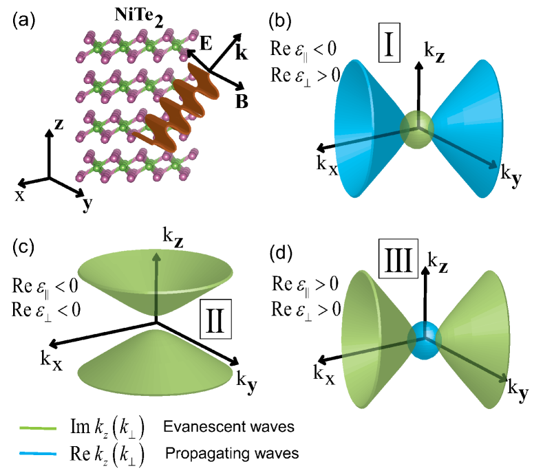
In this Letter, we unveil the unique EM response of NiTe2 in the near-infrared/optical range arising from its extreme anisotropy driven by the presence of Lorentz-violating Dirac fermions. In particular, we demonstrate that NiTe2 supports three photonic regimes with distinct topologies for evanescent waves (which have a rapidly decaying field amplitude in some spatial directions, such as surface plasmons) across the near-infrared/visible range. By tuning the optical frequency, NiTe2 can exhibit closed elliptical and two different kinds of open hyperbolic dispersion, as shown in Fig. 1. Exploiting electron energy loss spectroscopy and density functional theory, we identify multiple ENZ surface plasmons, exciting near photonic topological transitions (at about , , and eV), whose presence confirms the unusual topological photonic behavior of NiTe2. It is worth noting that surface plasmons display several significant features (viz., a resonant nature, strong light enhancement, and a high degree of confinement) and have been exploited in an enormous variety of applications wave ; lens ; ses . Finally, we show that the type-II Dirac bands are strongly involved in the origin of the ENZ surface plasmons. Thus, these findings establish NiTe2 as a suitable candidate for applications where an efficient manipulation of evanescent waves is crucial, viz., in nanophotonics, optoelectronics, imaging, and biosensing.
In order to highlight the different photonic regimes, we consider a polarized plane wave, with , , and excited inside a NiTe2 crystal. The dispersion relation for this EM mode is given by
| (1) |
Here, is the frequency-dependent in-plane/out-of-plane component of the dielectric permittivity tensor and is the speed of light in vacuum. The different regimes of the propagating ( is real) and evanescent ( is imaginary) EM wave can be deduced from the iso-frequency dispersion specified in Eq. (S6). Depending on whether ), we can get different topology of the iso-frequency surface of the propagating or evanescent waves. Specifically, we find that NiTe2 can support multiple regimes for the evanescent waves rapidly decaying perpendicular to the plane, as shown in Fig. 1. By tuning light frequency across the near-infrared/visible range, the dynamics of evanescent waves is described by either elliptical (I) or hyperbolic (II, III) dispersion relation (green surfaces in Fig. 1). In contrast, the bulk propagating waves have only hyperbolic (I) and elliptic (III) dispersion (cyan surfaces in Fig. 1). The bulk propagating waves are completely forbidden in the frequency regime where both . Together, these features make NiTe2 an ideal platform for harnessing the light-matter interactions in the deep-subwavelength regime Krishnamoorthy .
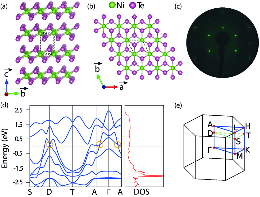
Bulk NiTe2 crystallizes in the CdI2 -type trigonal (1T) structure with space group (No. 164), as illustrated in Fig. 2(a) and (b). Details of the growth and characterization of single crystals with X-ray diffraction and Raman spectroscopy are reported in SM . The as-cleaved (001) surface displays a hexagonal surface symmetry, as evidenced by low-energy electron diffraction [LEED, shown in Fig. 2(c)]. The calculated band structure (Fig. 2d) displays the presence of a pair of type-II Dirac cones in the vicinity of the Fermi energy, along the axis. Angle-resolved photoemission spectroscopy experiments have confirmed the Dirac points to be located within meV above the Fermi energy, in addition to the presence of spin-momentum-locked surface states Ghosh_1 . The combination of hybridization of the Te-p orbital manifolds, crystal field splitting, and spin-orbit coupling (SOC) gives rise to multiple other topological features in NiTe2 over a wide energy range.
We evaluate the frequency-dependent dynamical dielectric functions in the long-wavelength limit , within the random phase approximation (RPA) Agarwal ; politano ; Sadhukhan . Specifically, starting from the generalized gradient approximation-based density functional theory, including the SOC, are calculated from an accurate Wannier tight-binding model of NiTe2 (see Supplementary Materials for details SM ).
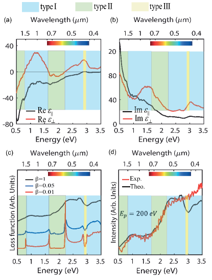
The unconventional EM response of NiTe2 is unveiled by the behavior of its frequency dependent dielectric functions, showing three distinct topological regimes (viz., I, II, and III as reported in Fig. 1) marked by green, blue and yellow region in Fig. 3, respectively. In the blue region of Fig. 3(a) and (b) [ eV and eV, and eV], we have and . Consequently, in these regions, the evanescent (propagating) waves experience an elliptic (hyperbolic) dispersion. In the regions depicted in green in Fig. 3, bounded by eV, and eV, we have and . Thus, in these regions, there are no propagating plane waves, though evanescent waves such as surface plasmons can be excited. In the relatively narrow spectral range eV, marked by yellow in Fig. 3, NiTe2 acts as an anisotropic positive dielectric medium, with . In this regime, the evanescent (propagating) waves exhibit the standard hyperbolic (elliptic) dispersion.
To probe the evanescent surface modes of NiTe2, we use electron loss energy spectroscopy (EELS), which is an ideal tool for detecting surface plasmons politano ; rocca1 ; rocca2 . Details of the experimental methods are presented in Supplementary Materials SM . EELS can probe surface plasmons when the electron penetration is negligible and the bulk modes are not excited, as for the case of low-energy impinging electrons (E 300 eV) in the reflection geometry. In a uniaxial crystal probed in the reflection geometry, the experimental EELS spectrum is theoretically reproduced by the surface loss function, Lam ,
| (2) |
Here, is the component of the electron velocity along the optical -axis, and (with ) is the geometrical average of the dielectric tensor components ( is the reduced Planck’s constant) Lam . The energy loss spectrum of Eq. (2) is peaked at a frequency for which , corresponding to the excitation of a surface plasmon (see SM for further details). We evaluate the surface loss function of Eq. (2) for NiTe2 by using the dielectric functions calculated from first principles reported in Fig. 3(a)-(b).
To reveal the connection between the different topological EM propagation regimes of NiTe2 and the experimental EELS spectrum, we investigate the case, where the imaginary parts of the dielectric components are diminished by a factor , viz., . We plot in Fig. 3(c), where (black, blue and red line, respectively). For small EM losses (), several peaks, coinciding with the topological transitions for EM propagation, clearly emerge in the spectrum. In particular, we find three peaks in the surface loss function at , , and eV, all of which lie near the boundary of the region where NiTe2 behaves as a negative dielectric medium (green shaded regions with both ). All three surface plasmon peaks arise from the anisotropic dielectric function of NiTe2, which in turn originates from the structural anisotropy and the resulting anisotropy in the electronic dispersion. Corresponding to high-momentum surface plasmon polaritons Warm , the condition for the existence of a surface plasmon is . This is exactly satisfied in the ideal case where the imaginary parts of dielectric functions are negligible for . As a consequence, in NiTe2 where , the surface plasmon resonances in NiTe2 are excited around the ENZ crossing points . Thus, the plasmonic resonances identify the ENZ conditions along with the location of the photonic topological transitions associated with the dispersion of evanescent waves as reported in Fig. 1(b) and (c). In addition to the three plasmon peaks arising in vicinity of , there are two additional peaks at the boundary of the yellow region (at about and eV) arising from the ENZ conditions (and ). These peaks correspond to the topological photonic transitions between the EM dispersion regimes reported in Fig. 1(b) and (d).
The experimental EELS spectrum is shown in Fig. 3(d), along with the theoretical loss function (for ). Our experimental results are in good agreement with the theoretical predictions, validating the occurrence of exotic topological photonic transitions in NiTe2. The measured spectra show two ‘flat’ regions (with reduced curve slope) approximately corresponding to the two hyperbolic zones eV and eV. The first flat region ( eV) arises from the superposition of the two surface plasmons exhibiting a relatively large resonance width, due to large EM losses (). The second flat region ( eV) arises from the superposition of the resonant surface plasmon at eV and the peak in the loss function related to the unusual ENZ response () of NiTe2. Note that surface plasmons are high-momentum evanescent waves (viz., ) Warm ; Zay and, generally, they are difficult to be excited in the standard metamaterials, since the effective medium theory does not hold when the EM momentum approaches the inverse size of the metamaterial inclusions. Thus, the desired metamaterial response can be completely washed out by the spatial scales associated with the metamaterial inclusions. In contrast, here, the presence of surface plasmons confirms that NiTe2 preserves the EM response even in the deep subwavelength regime.
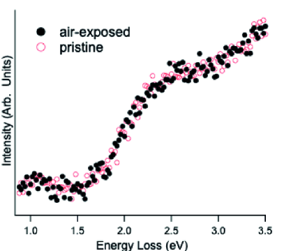
Considering the possible usage of the observed plasmonic modes for technological applications, we validated the robustness of the observed plasmonic modes in NiTe2. Furthermore, We conducted a systematic investigation of the dependence of the EELS excitation spectrum on the aging phenomena in the sample kept in air. The EELS spectrum does not display noticeable changes upon exposure to air, congruently with ambient stability inferred by AFM experiments (see SM for additional details).
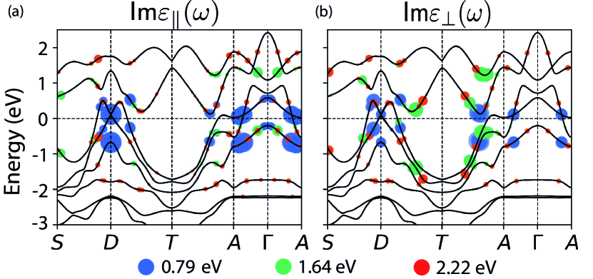
Finally, to physically grasp the origin of all the three surface plasmon modes, we focus on bulk dielectric function and its connection to the electronic bands. The imaginary part of the band and momentum resolved dielectric function (in the long wavelength limit) can be expressed as , with being the band index, representing a momentum point in the Brillouin zone (BZ). Here, we have defined the momentum and band resolved dielectric function,
| (3) | |||
In Eq. (Photonic Topological Transitions and Epsilon-Near-Zero Surface Plasmons in Type-II Dirac Semimetal NiTe2), is the Fermi function, represents the band dispersion of the th band, , denotes unit cell volume, and are the perpendicular/parallel () components of the velocity operator ( being the Hamiltonian of the system). Equation (Photonic Topological Transitions and Epsilon-Near-Zero Surface Plasmons in Type-II Dirac Semimetal NiTe2) captures the ‘strength’ of the vertical () interband electronic correlation () at the point in the BZ SM . Figure 4 shows the relative strength of , projected along the high symmetry directions in the BZ, for the three surface plasmon frequencies. In addition to contributions from higher conduction bands, the eV surface plasmon (red circles in Fig. 4) has spectral contributions arising from interband correlations involving the lowest conduction band hosting the Dirac fermions. The eV surface plasmon (green circles in Fig. 4) predominantly involves electronic correlations from the lower and the highest valance band ,including the Dirac bands, to higher conduction bands. The eV surface plasmon (blue circles in Fig. 4) has significant contribution arising from the interband electronic correlations involving the tilted type-II Dirac bands of NiTe2, in the vicinity of the Fermi energy.
In conclusion, we demonstrate that NiTe2 exhibits an unusual EM response in the near-infrared and visible frequency regime, driven by its huge intrinsic EM anisotropy and the presence of Lorentz-violating Dirac fermions. The isofrequency surfaces of evanescent EM waves in NiTe2 display several different photonic topologies, including one elliptical and two distinct hyperbolic dispersions. Our EELS experiments probe these photonic features as resonance peaks associated with the ENZ surface plasmons. Our study establishes NiTe2 and related materials can behave as hyperbolic, ENZ, and extremely anisotropic photonic materials with a ‘perfect’ homogeneous EM response even for highly confined surface waves. Overcoming some limitations of artificial composite metamaterials, topological semimetals, such as NiTe2, offer a novel pathway for engineering optical properties in the nanophotonic regime.
ACKNOWLEDGEMENT
B.G, D.D, and A.A thank the Science and Engineering Research Board and the Department of Science and Technology of the government of India for financial support. We thank the computer centre at IIT Kanpur, India for providing the high-performance computing facilities. The work at Northeastern University was supported by the Air Force Office of Scientific Research under award number FA9550-20-1-0322, and it benefited from the computational resources of Northeastern University’s Advanced Scientific Computation Center (ASCC) and the Discovery Cluster.
References
- (1) W. Cai and V. Shalaev, Optical Metamaterials: Fundamentals and Applications (Springer, Dordrecht, 2010).
- (2) R. Maas, J. Parsons, N. Engheta, and A. Polman, Nat. Phot. 7, 907 (2013).
- (3) M. Z. Alam, I. De Leon, R. W. Boyd, Science 352, 795 (2016).
- (4) I. Liberal, and N. Engheta, Nat. Phot. 11, 149 (2017).
- (5) J. Elser, R. Wangberg, and V. A. Podolskiy, Appl. Phys. Lett. 89, 261102 (2006).
- (6) A. Poddubny, I. Iorsh, P. Belov, and Y. Kivshar, Nat. Phot. 7, 948 (2013).
- (7) M. Coppolaro, M. Moccia, V. Caligiuri, G. Castaldi, N. Engheta, and V. Galdi, ACS Photonics 7, 2578 (2020).
- (8) A. Alu, Phys. Rev. B 84, 075153 (2011).
- (9) Hyperbolic metamaterials are extreme anisotropic crystals behaving as a metal along one direction and as a dielectric along the orthogonal direction.
- (10) M. Choe, K. H. Kim, and J. H. Wi, ChemPhysChem 22 92 (2021).
- (11) M. N. Gjerding, R. Petersen, T. G. Pedersen, N. A. Mortensen, and K. S. Thygesen, Nat. Comm. 8, 320 (2017).
- (12) S. Edalati-Boostan, C. Cocchi, and C. Draxl Phys. Rev. Materials. 4, 085202 (2020).
- (13) H. Gao, X. Zhang, W. Li, and M. Zhao, Opt. Expr. 27 36911 (2019).
- (14) Y. U. Lee, O. P. M. Gaudin, K. Lee, E. Choi, V. Placide, K. Takaishi, T. Muto, P. Andre, A. Muranaka, M. Uchiyama, F. Mathevet, T. Aoyama, J. Wu, A. D’Aleo, ad J.-C. Ribierre, ACS Photonics 6,1681 (2019).
- (15) J. Rho, Z. Ye, Y. Xiong, X. Yin, Z. Liu, H. Choi, G. Bartal, and X. Zhang Nat. Commun. 1, 143 (2010).
- (16) D. Lu, J. J. Kan, E. E. Fullerton, and Z. Liu Nat. Nanotech. 9, 48 (2014).
- (17) K. V. Sreekanth, K. H. Krishna, A. De Luca, and G. Strangi Scient. Rep. 4, 6340 (2014).
- (18) C. Simovski, S. Maslovski,I. Nefedov, S. Kosulnikov, P. Belov, and S. Tretyakov 2015 Photon. Nanostruct. 13 31 (2015).
- (19) C. Rizza, A. Ciattoni, E. Spinozzi, and L. Columbo, Opt. Lett. 37 3345 (2012).
- (20) N. Vasilantonakis, G. A. Wurtz, V. A. Podolskiy, and A. V. Zayats, Opt. Expr. 23, 14329 (2015).
- (21) X. Hu, K. P. Wong, L. Zeng, X. Guo, T. Liu, L. Zhang, Q. Chen, X. Zhang, Y. Zhu, K. H. Fung, and S. P. Lau, ACS Nano 14, 6276 (2020).
- (22) K. Sonowal, A. Singh, and A. Agarwal, Phys. Rev. B 100, 085436 (2019).
- (23) Z. Jalali-Mola, and S.A. Jafari, Phys. Rev. B 100, 205413 (2019).
- (24) K. Halterman, and M. Alidoust, Opt. Expr. 27, 36164 (2019).
- (25) O. J. Clark, M. J. Neat, K. Okawa, L. Bawden, I. Markovic, F. Mazzola, J. Feng, V. Sunko, J. M. Riley, W. Meevasana, J. Fujii, I. Vobornik, T. K. Kim, M. Hoesch, T. Sasagawa, P. Wahl, M. S. Bahramy, and P. D. C. King, Phys. Rev. Lett. 120, 156401 (2018).
- (26) M. S. Bahramy, O. J. Clark, B. J. Yang, J. Feng, L. Bawden, J. M. Riley, I. Markovic, F. Mazzola, V. Sunko, D. Biswas, S. P. Cooil, M. Jorge, J. W. Wells, M. Leandersson, T. Balasubramanian, J. Fujii, I. Vobornik, J. E. Rault, T. K. Kim, M. Hoesch, K. Okawa, M. Asakawa, T. Sasagawa, T. Eknapakul, W. Meevasana, and P. D. C. King, Nat. Mater. 17, 21 (2018).
- (27) T.-R. Chang, S.-Y. Xu, D. S. Sanchez, W.-F. Tsai, S.-M. Huang, G. Chang, C.-H. Hsu, G. Bian, I. Belopolski, and Z.-M. Yu, Phys. Rev. Lett. 119, 026404 (2017).
- (28) M. Yan, H. Huang, K. Zhang, E. Wang, W. Yao, K. Deng, G. Wan, H. Zhang, M. Arita, and H. Yang, Nat. Commun. 8, 257 (2017).
- (29) H. Huang, S. Zhou, and W. Duan, Phys. Rev. B 94, 121117 (2016).
- (30) C. Xu, B. Li, W. Jiao, W. Zhou, B. Qian, R. Sankar, N. D. Zhigadlo, Y. Qi, D. Qian, F.-C. Chou, and X. Xu, Chem. Mater. 30, 4823 (2018).
- (31) P. P. Ferreira, A. L. R. Manesco, T. T. Dorini, L. E. Correa, G. Weber, A. J. S. Machado, and L. T. F. Eleno, Phys. Rev. B 103, 125134 (2021).
- (32) L. Zhang, Z. Chen, K. Zhang, L. Wang, H. Xu, L. Han, W. Guo, Y. Yang, C.-N. Kuo, C. S. Lue, D. Mondal, J. Fuji, I. Vobornik, B. Ghosh, A. Agarwal, H. Xing, X. Chen, A. Politano, and W. Lu, Nat. Commun. 12, 1584 (2021).
- (33) M. Qi, C. An, Y. Zhou, H. Wu, B. Zhang, C. Chen, Y. Yuan, S. Wang, Y. Zhou, X. Chen, R. Zhang, and Z. Yang, Phys. Rev. B 101, 115124 (2020).
- (34) S. Nappini, D. W. Boukhvalov, G. D’Olimpio, L. Zhang, B. Ghosh, C.-N. Kuo, H. Zhu, J. Cheng, M. Nardone, L. Ottaviano, D. Mondal, R. Edla, J. Fuji, C. S. Lue, I. Vobornik, J. A. Yarmoff, A. Agarwal, L. Wang, L. Zhang, F. Bondino, and A. Politano, Adv. Funct. Mater. 30, 2000915 (2020).
- (35) B. Ghosh, D. Mondal, C.-N. Kuo, C. Shan Lue, J. Nayak, J. Fujii, I. Vobornik, A. Politano, and A. Agarwal, Phys. Rev. B 100, 195134 (2019).
- (36) Z. Wang, P. Guo, M. Liu, C. Guo, H. Liu, S. Wei, J. Zhang, X. Lu, ACS Appl. Energy Mater. 2, 3363 (2019).
- (37) Q. Liu, F. Fei, B. Chen, X. Bo, B. Wei, S. Zhang, M. Zhang, F. Xie, M. Naveed, X. Wan, F. Song, and B. Wang, Phys. Rev. B 99, 155119 (2019).
- (38) B. Zhao, W. Dang, Y. Liu, B. Li, J. Li, J. Luo, Z. Zhang, R. Wu, H. Ma, G. Sun, Y. Huang, X. Duan, X. Duan, J. Am. Chem. Soc. 140, 14217 (2018).
- (39) Y. Li, X. He, M. Guo, D. Lin, C. Xu, F. Xie, X. Sun, Sens. Actuators, B 274, 427 (2018).
- (40) R. F. Oulton,V. J. Sorger, D. A. Genov, D. F. P. Pile, and X. Zhang, Nat. Photonics 2, 496 (2008).
- (41) Y. Fu and X. Zhou, Plasmonics 5, 287 (2010).
- (42) M. Li, S. K. Cushinga, and N. Wu, Analyst 140, 386 (2015).
- (43) H. N. S. Krishnamoorthy, Z. Jacob, E. Narimanov, I. Kretzschmar, and V. M. Menon, Science 336, 205 (2012).
- (44) Supplemental Materials. Therein, we report details on the growth and characterization of single crystals with X-ray diffraction and Raman spectroscopy (Sec. S1). We provide further details on electronic structure and dielectric permittivity calculations (Sec. S2 and S3), EELS experiments (Sec. S4), theory of surface plasmons (Sec. S5), and ambient stability of NiTe2 (Sec. S6). Finally, we also report more details on the identification of interband electronic transitions involved in the surface plasmon excitations (Sec. S7).
- (45) A. Agarwal, M. S. Vitiello, L. Viti, A. Cupolillo, and A. Politano, Nanoscale 10, 8938 (2018).
- (46) A. Politano, G. Chiarello, B. Ghosh, K. Sadhukhan, C.-N. Kuo, C. S. Lue, V. Pellegrini, and A. Agarwal, Phys. Rev. Lett. 121, 086804 (2018).
- (47) K. Sadhukhan, A. Politano, A. Agarwal, Phys. Rev. Lett. 124, 046803 (2020).
- (48) B. Diaconescu, K. Pohl, L. Vattuone, L. Savio, P. Hofmann, V. M. Silkin, J. M. Pitarke, E. V. Chulkov, P. M. Echenique, D. Farias, and M. Rocca, Nature 448, 57 (2007).
- (49) M. Rocca, Surf. Sci. Rep. 22, 1 (1995).
- (50) Ph. Lambin, L. Henrard, P. Thiry, C. Silien, and J.P. Vigneron, J. Electron. Spectrosc. Relat. Phenom. 129, 281 (2003).
- (51) R. Warmbier, G. S. Manyali, and A. Quandt, Phys. Rev. B 85, 085442 (2012).
- (52) A. V. Zayats, I. I. Smolysniov, and A. A. Maradudin, Phys. Rep. 408, 131 (2005).
Supplementary Material
S1 Details of the growth and experimental characterization of a single crystal
Single-crystal growth
Single crystals of NiTe2 were grown using the Te flux method. We used various molar ratios of Ni to Te, ranging from to , finding an optimum ratio of . The mixtures of high-purity Ni powder () and Te ingots () were sealed under vacuum in a quartz tube with a flat bottom. The quartz ampule was heated to over hours, held at a constant temperature for hours, and then slowly cooled to at a rate of /h. It was finally annealed at this temperature for hours to improve the quality of the crystals. The remaining Te flux was removed by centrifuging above . Several shiny plate-like single crystals with typical sizes of mm3 were harvested, which could be easily cleaved with adhesive tape. The flat surface of the crystal corresponds to the plane.
XRD
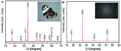
The crystal structure and phase purity of the as-grown crystals were identified by X-ray diffraction (XRD) (Bruker D2 PHASER) and Laue diffraction (Photonic Science) at room temperature. Figure S1 (a) shows the powder XRD pattern of NiTe2 samples, whose photograph is shown in the inset. Figure S1 (b) displays the single-crystalline XRD pattern from the (00l) planes of NiTe2. The inset represents the Laue diffraction taken along the (0001) direction.
Survey XPS spectrum of the as-cleaved sample
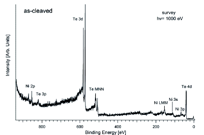
Figure S2 shows the survey XPS spectrum of the as-cleaved sample, validating its surface cleanliness. No trace of contamination is observed. In particular, O-1s and C-1s are totally absent.
Raman spectroscopy
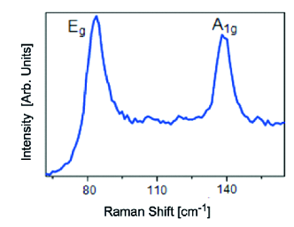
Phonon dispersion calculations were performed within the frozen-phonon method using the projector augmented wave (PAW) pseudopotentials and a plane basis set as implemented in VASP 11 ; 22 ; 33 . The cut-off for the plane-wave basis is set to eV and a -centered -grid was used for the BZ integration 44 . The exchange-correlation part of the potential was treated within the local density approximation (LDA) 55 . All the structures were properly relaxed until the force on each atom becomes vanishingly small. Below, we have tabulated the phonon frequencies of bulk NiTe2 in cm-1 at the -point, indicating their infrared or Raman activity based on our DFT calculations. The modes corresponding to and cm-1 are Raman active.
Thus, in NiTe2 there are phonon modes, acoustic, and optical. Only and are Raman active. Correspondingly, two Raman-active modes are observed experimentally (Fig. S3).
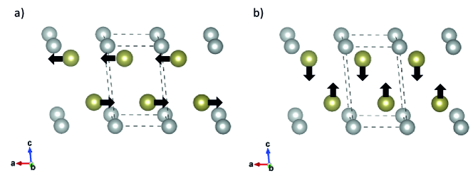
In Figure S4, we show a sketch of the displacements of the atoms, corresponding to the and one of the phonon modes. Note that both modes involve the motion of Te atoms primarily.
| Branch number | Frequency (cm-1) | Symmetry | Infrared (I)/ Raman (R) activity |
| 1-2 | 0.00 | - | |
| 3 | 0.00 | - | |
| 4-5 | 87.76 | R | |
| 6 | 150.30 | R | |
| 7 | 211.58 | I | |
| 8-9 | 227.66 | I |
S2 Details of the electronic structure calculations
To understand the electronic band structure of NiTe2, we perform a first-principle calculation using Vienna Simulation Package (VASP) 11 . The projector augmented wave (PAW) pseudopotentials have been adopted within the generalized gradient approximation (GGA) scheme developed by Perdew-Burke-Ernzerhof (PBE) 22 ; Perdew1996 . We have used kinetic energy cutoff of eV for the plane-wave expansion and a Monkhrost-Pack grid for the Brillouin zone integration mp_kgrid . Spin-orbit coupling (SOC) has been considered self-consistently.
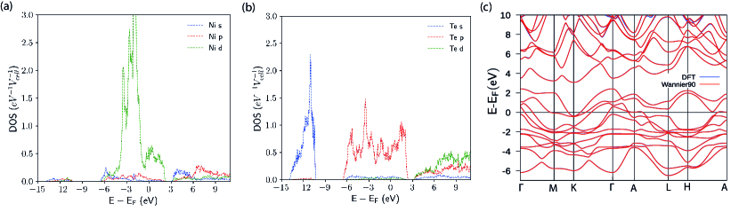
In order to numerically evaluate the dielectric tensor, we construct a tight-binding (TB) model based on maximally localized Wannnier functions (MLWF) Marzari2012 . To make a good Wannier model valid in a wide range of energies for the DFT bands, we have included all the dominant orbitals present in the required energy range as Wannier orbitals. The orbital resolved density of states for the electronic bands of NiTe2 over a wide energy range is shown in Fig. S5. Based on this, we have included the , , and orbitals of Ni and and orbitals for Te atoms.
S3 Dielectric function calculation
We have calculated diagonal components of frequency and momentum dependent dynamical dielectric tensor within random phase approximation (RPA) PhysRevB.73.045112 ; giuliani2005quantum
| (S1) |
Here, , denote the three cartesian components, and are the unit vectors along these directions. Here is the Fourier transform of Coulomb potential in three-dimension, with denoting the vacuum permittivity. In Eq. (S1), represents the noninteracting density-density response function or polarization, calculated along different directions.
To calculate the dielectric tensor, we first evaluate the dynamical form factorThygesen2011 by using the energy eigenvalues and eigenstates of the Wannier TB Hamiltonian with SOC,
| (S2) |
Here, and denote the momentum and energy transfer to the quasiparticle and is the energy eigenvalue for the state of the th band, and denotes the unit cell volume. Here the summation on runs over the first Brillouin zone (BZ) and the band occupancy is given by the Fermi distribution function, , with denoting the chemical potential. For simplicity, we work in the zero temperature limit for which the Fermi Dirac distribution function reduces to a step function, . Using the dynamical from factor in Eq. (S2), the non-interacting density-density response function is obtained by using Kramers-Kronig transformation Thygesen2011 ,
Here, is a small broadening parameter. We have used a relatively dense -grid of in the calculation of the non-interacting response function. Then, we compute the dynamical dielectric tensor using Eq. (S1). The direction of the momentum transfer is chosen along specific high-symmetry directions in the Brillouin zone like , etc. Depending on the direction of , we have computed different components of dielectric tensor as , , and . The rotational in-plane symmetry of the NiTe2 crystal structure forces . However, the out-of-plane component of the dielectric tensor, turns out to be different than the in-plane component due to the layered structure of NiTe2.
S4 EELS experiments
The reflection EELS experiments were carried out at room temperature using an EELS apparatus with two mm hemispherical deflectors for both monochromator and rotating analyzer, mounted in an ultrahigh-vacuum chamber at the University of Calabria, Italy. All experiments were made in a base pressure mbar. Spectra were acquired with an incident electron beam positioned at a fixed angle of 45∘ with respect to the surface normal. The kinetic energy of the incident electrons was 200 eV. For these experiments, scattered electrons were collected in specular reflection condition, with an angular acceptance of 2∘. A medium energy resolution of meV was set to achieve the best signal-to-noise ratio.
S5 Surface Plasmons in a uniaxial crystal
Let us consider a system consist of a semi-infinite slab and a vacuum region, located in the half-space and , respectively. The slab is a uniaxial crystal, where the -axis is the crystal optical axis, and its dielectric permittivity tensor is . Here, we discuss surface plasmons (SPs) supported by a uniaxial crystal (like NiTe2). SPs belong to a subclass of SP polaritons, namely special -polarized plane waves propagating along the vacuum-slab interface, whose amplitudes decay away from the interfaceZay . Without loss of generality, we search monochromatic plane waves of the kind , propagating along the -axis. The dispersion relations, describing the propagation of a -polarized plane wave in the considered system, are
| (S3) |
and
| (S4) |
in vacuum and inside the uniaxial crystal, respectively, where , are the complex wave vectors along the -axis. Imposing the standard interface boundary conditions (the continuity of the electric and the magnetic field parallel to the vacuum-slab interface), we get the relationWarm ,
| (S5) |
In the static limit (i.e., ), Eq.(S3) and Eq.(S4) imply
| (S6) |
Finally, imposing that the SP amplitudes exponentially decay away from the interface [ and, ], and considering Eq. (S6), we get
| (S7) |
Equation (S7) represents the existing condition of an SP supported by a uniaxial crystal, and it can be exactly satisfied in the situation where the imaginary part of the dielectric functions are negligible. In this idealistic case, the SPs are excited for in the region where and . As reported in the main text, the resonances appearing in the electron energy loss spectroscopy (EELS) spectrum, given by the condition , are clearly associated with the excitation of SPs.
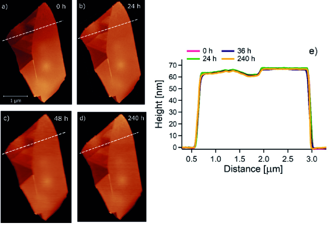
S6 Ambient stability
To evaluate the environmental stability of NiTe2, the evolution of atomic force microscopy (AFM) images of mechanically exfoliated flakes [Figs. S6(a)-(d)] was followed on a timescale of up to days. The AFM results demonstrate that exposure to the atmosphere does not change the morphology of the flakes, as confirmed by the height profile along a specific direction remaining constant with exposure [Fig. S6(e)]. In addition, the EELS spectrum does not display noticeable changes upon exposure to air, congruently with ambient stability inferred by AFM experiments (see Fig. S7).
S7 Connection with interband transitions
The calculated surface loss spectrum shows three surface plasmon modes at about 0.79 eV, 1.64 eV and 2.22 eV. To trace the origin of these modes, we focus on the imaginary part of the dielectric tensor in the long-wavelength limit (). The imaginary part of the dielectric tensor is associated with inter-band transitions, and it can indicate which pair of bands are involved in the transitions corresponding to the surface plasmon energies.
In the long-wavelength limit, the total dielectric function can be expressed as Jia_2020 ,
Here, denotes the velocity operator. Here and represents small broadening parameter for intraband and interband contributions, respectively. The imaginary part of the interband dielectric function in Eq. (LABEL:varepsilon_q0) is given by,
| (S9) |
where,
| (S10) |
Using the momentum resolved imaginary part of the dielectric tensor for corresponding to the plasmon frequencies, we can identify the bands and the specific points of the BZ which contribute most to the vertical interband electronic transitions. In Fig. 4 of the main text, we have shown the distribution of projected along the high symmetric direction in the BZ for three plasmon peaks at 0.79 eV, 1.64 eV and 2.22 eV.
References
- (1) G. Kresse, J. Furthmuller, Phys. Rev. B, 54, 11169 (1996).
- (2) G. Kresse, D. Joubert, Phys. Rev. B 59, 1758 (1999).
- (3) A. Togo, I. Tanaka, Scr. Mater., 108, 1 (2015).
- (4) P. E. Blochl, O. Jepsen, O. K. Andersen, Phys. Rev. B, 49, 16223 (1994).
- (5) W. Kohn, L. J. Sham, Phys. Rev. 140, A1133 (1965).
- (6) J. P. Perdew, K. Burke, and M. Ernzerhof, Phys. Rev. Lett. 77, 3865 (1996).
- (7) H. J. Monkhorst and J. D. Pack, Phys. Rev. B 13, 5188 (1976).
- (8) N. Marzari, A. A. Mostofi, J. R. Yates, I. Souza, and D. Vanderbilt, Rev. Mod. Phys. 84, 1419 (2012).
- (9) A. V. Zayats, I. I. Smolysniov, and A. A. Maradudin, Phys. Rep. 408, 131 (2005).
- (10) R. Warmbier, G. S. Manyali, and A. Quandt, Phys. Rev. B 85, 085442 (2012).
- (11) M. Gajdos, K. Hummer, G. Kresse, J. Furthmuller, and F. Bechstedt, Phys. Rev. B 73, 045112 (2006).
- (12) G. Giuliani and Vignale, Quantum Theory of the Electron Liquid (Cambridge University Press, 2005).
- (13) J. Yan, J. J. Mortensen, K. W. Jacobsen, and K. S. Thygesen, Phys. Rev. B 83, 245122 (2011).
- (14) X. Jia, M. Wang, D. Yan, S. Xue, S. Zhang, J. Zhou, Y. Shi, X. Zhu, Y. Yao, and J. Guo, New Journal of Physics 22, 103032 (2020).