Separation of Artifacts from Spin-Torque Ferromagnetic Resonance Measurements of Spin-Orbit Torque for the Low-Symmetry van der Waals Semi-Metal ZrTe3
Abstract
Spin-orbit torques generated by exfoliated layers of the low-symmetry semi-metal ZrTe3 are measured using the spin-torque ferromagnetic resonance (ST-FMR) technique. When the ZrTe3 has a thickness greater than about 10 nm, artifacts due to spin pumping and/or resonant heating can cause the standard ST-FMR analysis to overestimate the true magnitude of the torque efficiency by as much as a factor of 30, and to indicate incorrectly that the spin-orbit torque depends strongly on the ZrTe3 layer thickness. Artifact-free measurements can still be achieved over a substantial thickness range by the method developed recently to detect ST-FMR signals in the Hall geometry as well as the longitudinal geometry. ZrTe3/Permalloy samples generate a conventional in-plane anti-damping spin torque efficiency = 0.014 0.004, and an unconventional in-plane field-like torque efficiency = 0.003 0.001. The out-of-plane anti-damping torque is negligible. We suggest that artifacts similarly interfere with the standard ST-FMR analysis for other van der Waals samples thicker than about 10 nm.
keywords:
Spin-torque ferromagnetic resonance, Spin-orbit torque, Spin pumping, Resonant heating, van der Waals, ZrTe3Thow Min Cham, Saba Karimeddiny, Vishakha Gupta, Joseph A. Mittelstaedt and Daniel C. Ralph∗
Thow Min Cham, Saba Karimeddiny, Vishakha Gupta, Joseph A. Mittelstaedt,
Prof. Daniel C. Ralph
Department of Physics, Cornell University, Ithaca, NY 14850, USA
Email Address: dcr14@cornell.edu
Prof. Daniel C. Ralph
Kavli Institute at Cornell, Ithaca, NY 14853, USA
1 Introduction
Spin-orbit torques can provide efficient switching of magnetization in nanoscale magnetic
devices.[1, 2, 3] The torques generated by the heavy metals Pt,[4, 5, 6, 7, 8, 9, 10] Ta,[11, 12, 13] W[14, 15] and their alloys[16, 17] have been studied in detail.
More recently, spin-orbit torques generated by van der Waals materials have been an increasing focus, in order to study the consequences of spin-momentum coupling in topological materials and to generate spin-orbit torques with unconventional orientation using low-symmetry materials.
Recent experiments in these categories include studies of transition metal dichalcogenides (TMDs) MoS2,[18, 19, 20] WTe2,[21, 22, 23, 24] WS2,[25] NbSe2,[26]
TaTe2,[27]
MoTe2,[28, 29, 30] PtTe2,[31] TaSe2,[32] WSe2,[33, 34] and Cd3As2,[35] as well as studies of the topological insulators Bi2Se3,[36, 37, 38] BiSb[39] and magnetically-doped BiSbTe.[40, 41]
When devices are made from exfoliated samples of van der Waals materials, it can sometimes be difficult to isolate layers thinner than a few 10’s of nanometers, so the spin-orbit layers can be much thicker than for typical measurements of heavy metals, where the spin-orbit layers are generally much thinner than 10 nm. Here we illustrate using ZrTe3/Permalloy bilayers that extra care is required when employing the spin-torque ferromagnetic resonance (ST-FMR) technique[6, 42, 43, 44] in devices with thicker spin-orbit layers, because the magnitude of artifacts due to spin pumping[45, 46, 47] and resonant heating[48] grow relative to the spin-orbit-torque signals as a function of increasing layer thickness. One signature of such artifacts is an apparent dependence of the spin-torque efficiency on the spin-orbit layer thickness for layers much thicker than a typical spin diffusion length. We demonstrate that a recently-introduced modification of the ST-FMR technique,[49] in which the ST-FMR signals are measured in the Hall geometry as well as the usual longitudinal geometry,[50, 51] allows more-accurate measurements of the spin-orbit torques, separated from artifacts due to spin pumping and resonant heating, without any significant added experimental effort.
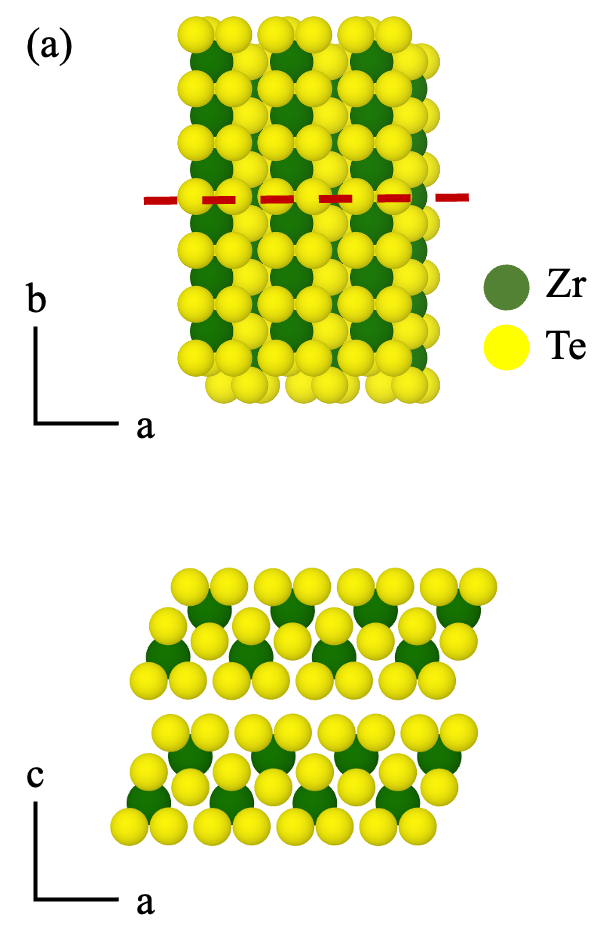
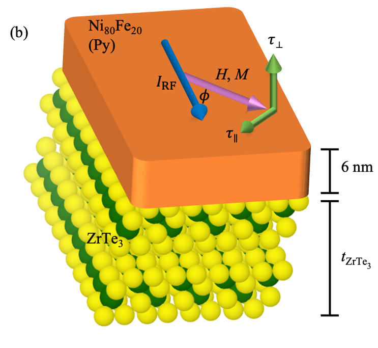
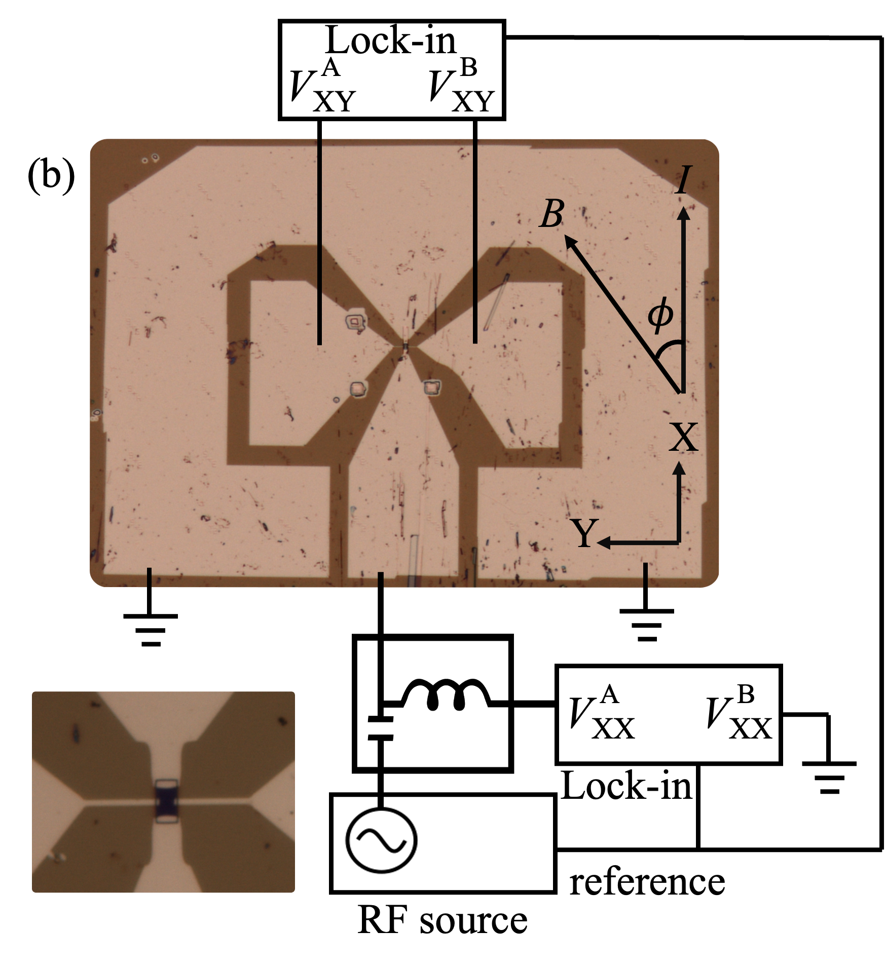
ZrTe3 has the space group P21/m (no. 11), with a screw axis along the Zr chain and a mirror plane perpendicular to the screw axis[52, 53] as shown in Figure 1a. ZrTe3 flakes exfoliate into narrow nano-ribbons extended along the b axis, perpendicular to the a-c mirror plane, with typical dimensions of x . The crystal axis of the exfoliated flakes can be easily identified by the orientation of the nano-ribbons. We prepare spin-orbit-torque test structures of ZrTe3 with varying thicknesses capped with 6 nm of Permalloy (Py, Ni80Fe20). To avoid air exposure of the ZrTe3, we perform the final step of exfoliation in the load-lock chamber of our sputter system, at pressures 10-6 torr. We then deposit the Py via magnetron sputtering without breaking vacuum. The Py has in-plane magnetic anisotropy. Figure 1b shows a schematic of the Py-covered ZrTe3 heterostructure. We have studied two types of device geometries made by electron-beam lithography and ion milling (see the Experimental Section): standard ST-FMR bars in which only longitudinal electrical signals can be measured (Figure 2a) and ST-FMR devices which also contain Hall contacts (with side wires) (Figure 2b). The devices with Hall contacts allow a separation of spin-orbit-torque signals from artifacts due to spin pumping and resonant heating.
2 Results
For our ST-FMR measurements, we use a microwave-frequency (9-12 GHz) current source to generate current-induced torques on the Py magnetic layer while sweeping an in-plane magnetic field at a fixed angle (Figure 1b). When the magnetic field is swept through the resonance condition, the resulting magnetic precession produces resistance oscillations that mix with the applied current to create a DC voltage signal. In addition to this mixing signal, resonant DC voltages that we will describe as artifact voltages can also be generated by (i) spin pumping of spin current from the magnetic layer to the spin-orbit layer together with the inverse spin Hall effect in the spin-orbit layer, (ii) resonant heating that generates a spin Seebeck-induced spin current into the spin-orbit layer together with the inverse spin Hall effect, and (iii) resonant heating that generates a thermal gradient within the conducting magnetic layer together with the Nernst effect. In all cases, these artifacts result in an electric field at resonance that is perpendicular to the magnetization axis, so that the artifacts produce voltage signals sharing same dependence on the angle . We modulate the amplitude of the microwave-frequency current source at 1 kHz and detect the resonant voltage from the sample using a bias tee and lock-in amplifier.
We will analyze the results from our ST-FMR measurements first using an (incorrect) “standard” analysis framework that neglects the contributions from spin pumping and resonant heating. We will then demonstrate the framework that considers both the longitudinal and Hall-detected resonance voltages, and that allows the artifact signals to be separated from the mixing signal due to the spin-orbit torques.
2.1 Analysis neglecting artifacts
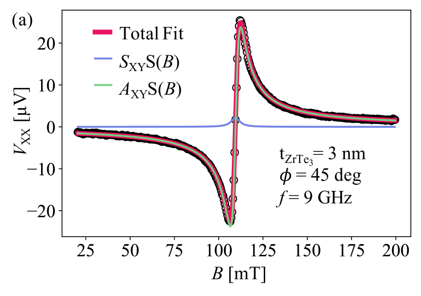
Within the standard ST-FMR analysis framework, only the longitudinal voltage parallel to the applied current is detected. We fit this resonant voltage to a sum of symmetric and anti-symmetric Lorentzian components, plus a linear background to account for the ordinary Nernst effect (ONE)
| (1) |
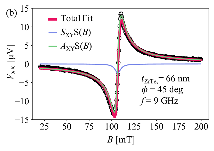
Here we define the symmetric and anti-symmetric Lorentzians as S() = and A() = where is the resonant field and is the linewidth. Fits to the data taken at = 9 GHz and = 45 deg in Figure 3a,b, show good agreement for both thin (3 nm) and thick (66 nm) ZrTe3. These data can be analyzed within the framework of the Landau-Lifshitz-Gilbert-Slonczewski equation,[54] assuming a magnetic layer with in-plane anisotropy and that macrospin magnetic dynamics are a good approximation[55]
| (2) |
where is the orientation of the magnetic moment, is an effective magnetic field, is the gyromagnetic ratio, is the Gilbert damping parameter ( where is the resonance angular frequency), and and are the in-plane and out-of-plane current-induced torques per unit magnetic moment. If one assumes that the signal is entirely due to the mixing voltage, with no contribution from the artifact voltages, then the amplitudes of the Lorentzian components and depend on the strengths of and [21]
| (3) |
| (4) |
where is the applied GHz current and the change in the resistance of the bilayer as a function of in-plane magnetization orientation is cos. We define = , = + , , and = + . is the resonant field and is the perpendicular anisotropy field (positive for a film with in-plane anisotropy).
For high-symmetry spin-orbit materials, the in-plane torque from the spin current , is constrained by symmetry to have the anti-damping form , ( for Pt), so that for an in-plane magnetization , while the out-of-plane torque can be the sum of a field-like spin-orbit torque and the torque due to the Oersted field , both of which give . Therefore in this simple case, both and are proportional to . For a low-symmetry material like ZrTe3, current-induced spins oriented in the direction are also allowed by symmetry if there is a component of current perpendicular to the mirror plane.[21, 22, 28, 56, 53] This allows for an in-plane field-like torque of the form and an out-of-plane anti-damping torque of the form so that for an in-plane magnetization and . Consequently, the amplitudes of the ST-FMR components can have the angular dependence
| (5) |
| (6) |
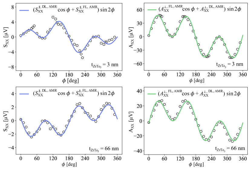
where , , , and are constants corresponding to the strength of the , , and torques respectively. Fits to the angular dependence for 3 nm and 66 nm thick ZrTe3 devices in Figure 4 show good agreement with the expected angular dependence. For the thinner ZrTe3 layer we observe a non-zero value of corresponding to an unconventional in-plane field-like torque. An unconventional out-of-plane anti-damping torque is allowed by symmetry, but is not evident in the angular fits for either sample.
If one assumes that the out-of-plane field-like spin-orbit torque is negligible relative to the Oersted torque (a good assumption at least for the thicker ZrTe3 layers, see the Supporting Information), one can calculate the efficiencies corresponding to the in-plane torques and by using the Oersted torque to calibrate the charge current density in the ZrTe3 layer[6]
| (7) |
| (8) |
Here is the saturation magnetization, is the ZrTe3 thickness, and is the Py thickness. We have also checked this approach for selected sample thicknesses by directly calibrating the microwave current in the sample using a vector network analyzer (see Supporting Information), rather than computing , and the conclusions are the same.
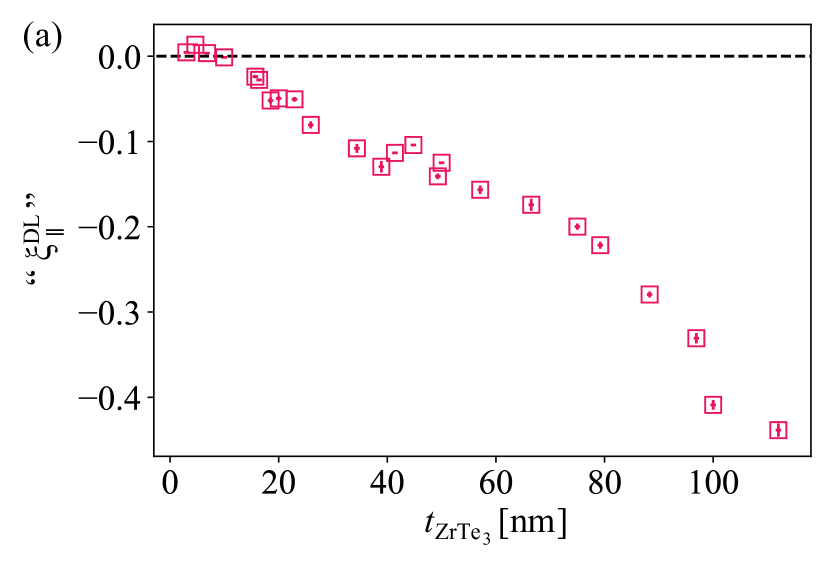
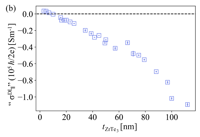
The results of this (incorrect) standard analysis, which neglects artifact effects, are shown in Figure 5a as a function of the thickness of the ZrTe3 layer. For the thinnest ZrTe3 layers, the standard in-plane anti-damping torque efficiency is weakly positive, with a value for the 3 nm ZrTe3 layer, but as a function of increasing ZrTe3 thickness it becomes negative, with strong thickness dependence through 100 nm. At the largest ZrTe3 thicknesses, the apparent magnitude of appears to become extremely large 0.4, even larger than the value for pure W.[14] The corresponding torque conductivity (Figure 5b), also exhibits the unusual thickness dependence and very large apparent values, on the same order of magnitude as Pt for the thickest ZrTe3 samples, 105 () Sm-1.[16] The unconventional in-plane fieldlike torques have values around and remain largely independent of ZrTe3 thickness (Figure 5c), while the out-of-plane anti-damping torques are negligible (Figure 5d).
This standard analysis is incorrect because of the neglect of the artifacts from spin pumping[45, 46, 47] and resonant heating[48]. The Oersted torque generated by the charge current in the ZrTe3 layer is proportional to charge current density in the layer times the ZrTe3 layer thickness, while the spin-orbit torques are proportional only to the charge current density. Consequently, as the ZrTe3 layer thickness increases the Oersted torque increasingly dominates over the spin-orbit torques. The large Oersted torque generates large precession amplitudes, and hence increased signals due to spin pumping and resonant heating, relative to the mixing voltages generated by the spin-orbit torques. These artifact voltages produce a symmetric resonant peak shape, and when the ST-FMR resonant voltage is detected only in the longitudinal direction they have the same angular dependence as the signal from the in-plane anti-damping spin-orbit torque, and hence cannot be distinguished from the mixing signal due to . For the sign of in Py devices, the sign due to the spin-pumping signal is opposite to the rectification signal due to ,[49] consistent with Figure 5a, and the magnitude of the signals we observe in Figure 5a are also fully consistent with expectations for the spin pumping + inverse spin Hall effect (see Supporting Information).
2.2 Using ST-FMR in the Hall geometry to separate the spin-orbit-torque signal from artifacts
When ST-FMR signals are detected in the Hall geometry in addition to the standard longitudinal geometry, the angular dependence of artifacts due to spin-pumping and resonant heating is no longer identical to the Hall-detected spin-orbit mixing signal, allowing the different signals to be separated.[49] We perform the Hall-detected measurements using the sample geometry shown in Figure 2b. We detect both the transverse and longitudinal voltage signals at the same time using two lock-in amplifiers registered to the same kHz-frequency amplitude modulation of the microwave-frequency applied current. Neither the device fabrication nor the measurements themselves therefore take more time than conventional longitudinal ST-FMR measurements. To obtain quantitative values of the current-induced torques, we calibrate the microwave current for each device using a vector network analyzer (see Supporting Information).
We follow the analysis procedure described in reference [49] with the addition of contributions from the unconventional torques and . The transverse ST-FMR signal can again be separated into symmetric and anti-symmetric Lorentzian components, = S() + A() (Figure 6).
The artifact-induced voltages have the angular dependence:
| (9) | ||||
where is the length of the device (in the longitudinal direction) and is the width, and we have used the relations cos2sin = (sin2cos)/2 and cos3 = (cos + cos2cos)/2. We add these contributions from the artifact-induced voltages to the mixing voltages from current-induced magnetic precession. The mixing voltages in the Hall geometry have contributions from modulation of both the planar and anomalous Hall effects, () = sinsin()cos() + R cos(), times angular dependence associated with and (see the derivation in [49]). Here is the tilt angle of the magnetization relative to the out-of-plane direction. The general form of the dependence for the case in which current-generated spins are allowed in both the and directions is
| (10) | ||||
with the amplitude coefficients
| (11) | ||||
Here we have assumed that the unconventional components of the spin Hall conductivity are sufficiently small that they do not influence the angular dependence of the artifact voltage.
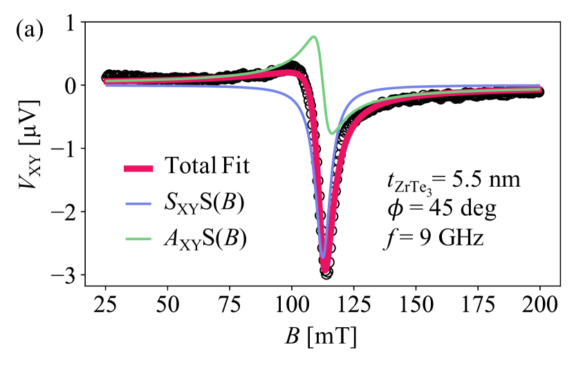
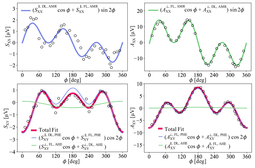
Figure 7 shows representative fits of Equation (10) to the measured angular dependence of , , , and for a ZrTe3 (5 nm)/Py (6 nm) sample. We find good agreement. We can determine the artifact electric field by first calculating the ratio in two different ways by employing the pair of parameters and associated with each of the AMR, PHE, and AHE corresponding to and
| (12) |
| (13) |
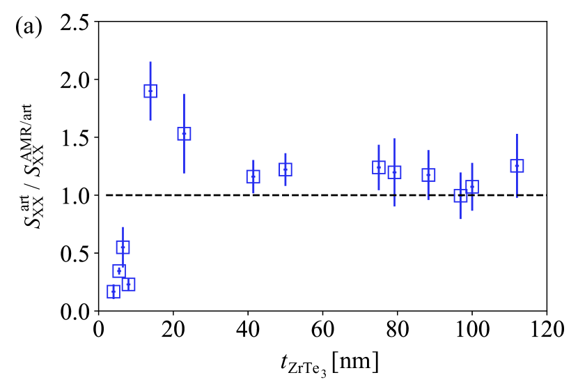
Using the measured amplitude coefficients, one can solve for using either Equation (12) or (13) and check consistency (see Supporting Information for details about the sign in the quadratic formula). We find that these values do agree to within experimental uncertainty. Figure 8a shows the ratio of the artifact voltage to the total measured value of . We see for ZrTe3 layers thicker than 10 nm that this ratio is close to 1, meaning that the longitudinal symmetric ST-FMR signals are completely dominated by the artifact voltage.
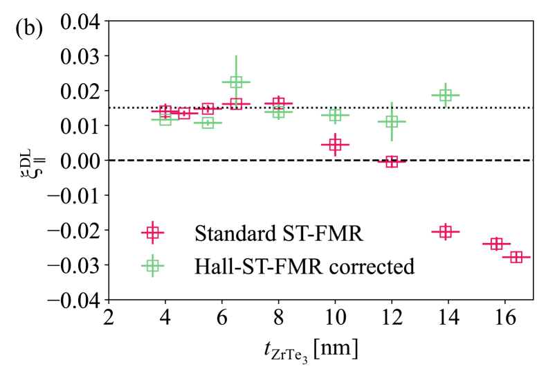
Figure 8b shows the results of the Hall ST-FMR analysis for the efficiency of the conventional in-plane anti-damping spin-orbit torque, separated from the artifact signals. To arrive at these values, we determine by subtracting the artifact voltage from the measured values of in Equation (11), measuring from the ST-FMR linewidths, from the frequency dependence of (assuming ), and calibrating for each device using a vector network analyzer. The in-plane anti-damping spin-torque efficiency is then determined from using Equation (7) using a parallel-resistor model to estimate the charge current density within the ZrTe3 layer.
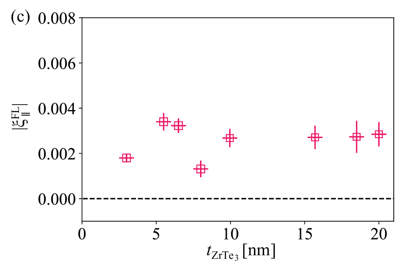
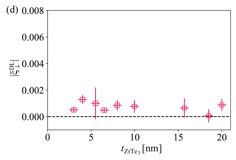
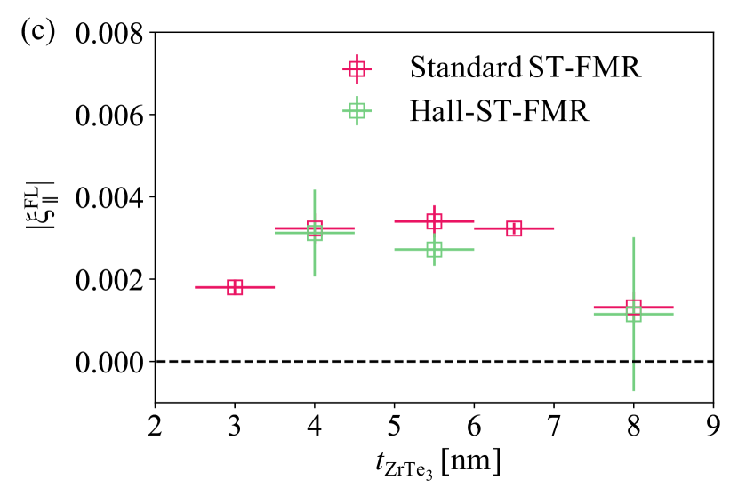
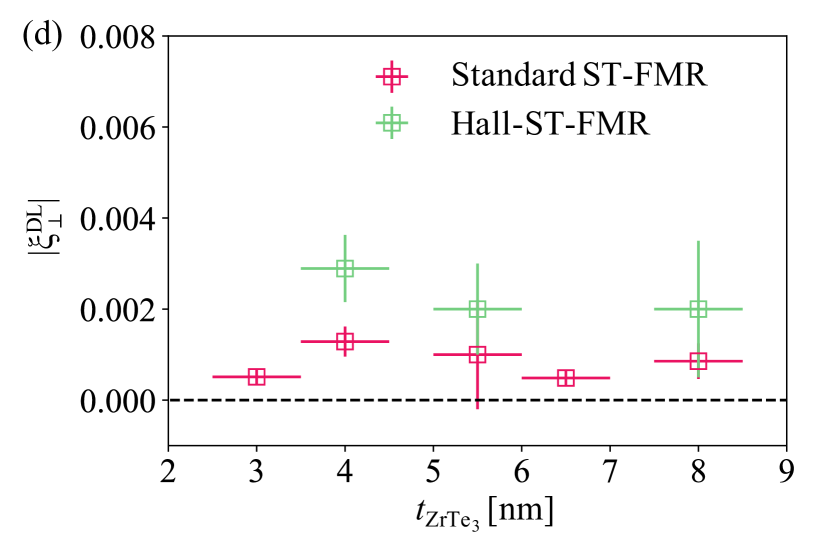
We obtain the efficiency = 0.014 0.004 as shown by the dotted line in figure 8, largely independent of device thickness for 15 nm. Beyond ZrTe3 thicknesses of 15 nm, the artifact voltages are too large to make an accurate determination of the spin-orbit torque, but it is clear that the apparent thickness dependence of this efficiency in the range 15 nm in Figure 5a is due entirely to the effects of the artifact voltages. The unconventional torques from the Hall geometry (Figure 8c,d), also remain largely independent of thickness, with values that are little-changed from the conventional ST-FMR analysis.
3 Conclusion
We have used ST-FMR to investigate the spin-orbit torques generated by exfoliated flakes of the low-symmetry semi-metal ZrTe3 for a wide range of layer thicknesses in ZrTe3/Py(6 nm) devices. We find that the “standard” ST-FMR analysis, which neglects the effects of artifacts due to spin pumping and resonant heating, gives incorrect values for the in-plane anti-damping torque efficiency of ZrTe3 layers thicker than about 10 nm. For the thickest layers, this incorrect standard analysis can overestimate the magnitude of by as much as a factor of 30, and it indicates an unphysical strong dependence of the torque efficiency on layer thickness. ST-FMR measurements in the Hall geometry demonstrate that this strong apparent thickness dependence is due entirely to artifacts from spin pumping and/or resonant heating, not a true dependence of the spin-orbit torque on layer thickness. For ZrTe3, the Hall ST-FMR measurements yield torque efficiencies = 0.014 0.004 for the conventional in-plane anti-damping torque and = 0.003 0.001 for the unconventional in-plane field-like torque. The unconventional spin-orbit torques in ZrTe3 are similar to strained NbSe2 in that the in-plane field like torque is non-zero while the out-of-plane anti-damping torque is negligible, while low-symmetry WTe2 and MoTe2 are different in that the out-of-plane anti-damping torque is non-zero.
We can make an estimate for when artifact voltages cannot be neglected for an arbitrary nonmagnetic (NM) spin-source material by calculating the ratio of the longitudinal spin-pumping voltage (Eq. (1) in the Supporting Information) divided by the mixing voltage associated with the conventional in-plane antidamping torque (Eq. (4) in the main text.) To simplify the approximation, we consider the case where the Oersted field is the primary driver of the precession that generates the spin-pumping voltage, that the applied magnetic field can be neglected relative to , and that the scale of the magnetoresistance varies with the NM layer thickness as , where is the magnetoconductance in the limit of zero NM-metal thickness and is the total device resistance. We also assume that the thickness of the NM layer is greater than the spin diffusion length, . After some algebra, we obtain
| (14) |
Here is the resistivity of the nonmagnetic material, is the effective spin-mixing conductance of the interface, and is an interface transparency for spin currents going from the nonmagnet to the magnet that we approximate 1. We note that has no dependence on the value of the spin Hall torque efficiency as long as this is non-zero. The relative importance of the spin-pumping artifact grows with layer thicknesses and . For parameters appropriate for our ZrTe3/Py samples, = 5.7 x 10⁻⁶ m, T, = 6 nm, , and = 1 x 10⁻⁵ , and for typical values = 2 x 10¹⁹ m-2 and = 2 nm, we obtain 0.2 for a 10 nm ZrTe3 layer and 20 for a 100 nm device, reasonably consistent with our measurements. If the parameters of the magnetic layer are fixed, then by Eq. (14) the crossover thickness of the normal metal beyond which spin pumping cannot be neglected scales as
| (15) |
Because of the square root, the crossover thickness is only weakly dependent on the properties of the nonmagnetic layer. We conclude, as a rule of thumb, that the effects of spin-pumping signals should not be ignored in any conventional ST-FMR experiment that employs nonmagnetic layers approaching 10 nm or above.
Several previous experiments studying spin-orbit torques generated by van der Waals layers have performed a conventional ST-FMR analysis, without accounting for the possibility of artifacts due to spin pumping or resonant heating, for devices with layers considerably thicker than 10 nm.[24, 30, 31] They have reportedly unexpectedly large values for the spin-torque efficiencies compared to thinner layers[21, 22, 28] and strong thickness dependence in the torque efficiency in this large-thickness range beyond 10 nm – qualitatively similar to what we find in our ZrTe3 samples when we neglect artifacts. We suggest that these anomalous results are due to spin pumping and/or resonant-heating artifacts, and that these measurements therefore do not provide accurate values of spin-orbit torques. We also suggest that ST-FMR measurements in the Hall geometry should be adopted as a standard technique to allow a clear separation of true spin-orbit-torque signals from these artifacts.
4 Experimental Section
4.1 Device Fabrication and Characterization
We make spin-orbit-torque test structures by first using the scotch-tape exfoliation method to transfer flakes from bulk ZrTe3 crystals bought commercially from HQ-Graphene, onto high-resistivity silicon/silicon dioxide (300 nm) wafers in a nitrogen glove box with H2O and O2 levels 0.5 ppm. For the final stage of exfoliation, scotch-tape covered crystals are transferred into the load lock of a magnetron sputtering system, where pristine surfaces of ZrTe3 are exfoliated under a vacuum of 10-6 torr. We then use grazing angle sputtering to deposit 6 nm of Permalloy (Py, Ni80Fe20) and 2 nm of aluminum to cap the film. The aluminum cap is oxidized upon exposure to air. Flakes of appropriate thicknesses are then screened using optical contrast, and selected based on the results of atomic force microscopy (AFM). Figure 1b shows a schematic of the Py-covered ZrTe3 heterostructure.
Regions of flakes to be incorporated into devices for study are chosen so that they are smooth ( 0.3 nm roughness) with no mono-layer steps and are free of residue from the exfoliation process. We pattern bars along length of the ZrTe3 nano-ribbons, parallel to the b axis and perpendicular to the mirror plane, with typical dimensions of 6 4 m2, using electron-beam lithography and ion-milling. Electrical contacts for ST-FMR measurements are made using a second round of e-beam lithography and magnetron sputtering of 5 nm Ti/60 nm Pt. We have studied two types of device geometries: standard ST-FMR bars in which only longitudinal electrical signals can be measured (Figure 2(a)) and ST-FMR devices which also contain Hall contacts (with 1 m side wires) (Figure 2(b)). The crystallographic orientations of the ZrTe3 in the completed devices are further confirmed using polarized Raman spectroscopy on a WITec Alpha300R confocal Raman microscope fitted with a Thorlabs rotation stage (see Supporting Information).
4.2 ST-FMR Measurement
ST-FMR measurements were done using an Agilent E8257C 40 GHz rf power source and Signal Recovery 7265 Lock-in amplifiers for readout of the mixing voltages. RF signals with frequencies 9-12 GHz were input with a maximum power of 10 dBm along the low symmetry b axis of the ZrTe3/Py heterostructures. In-plane magnetic fields were applied on a probe station using a GMW 5201 projected field magnet mounted on x, y and phi motion stages controlled by a Newport ESP300 motion controller. Fields were swept from 0 - 0.27 T at varying in-plane angles () with respect to the current direction while keeping the rf frequency constant. The rf current calibration was done through S and S measurements using an Agilent 8722ES 40 GHz Network Analyzer.
Supporting Information
Supporting Information is available from the Wiley Online Library or from the author.
Acknowledgements
We acknowledge helpful discussions with Arnab Bose and Rakshit Jain, and nano-fabrication advice and measurement support from Jeremy Clark and Steve Kriske. Primary support for research expenses came from the US Dept. of Energy (DE-SC0017671). T.M.C. led the sample fabrication, measurement, and analysis, supported by the Singapore Agency for Science, Technology, and Research. S.K. assisted with calibrations and data analysis, supported by the NSF (DMR-1708499). Assistance with deposition of the heterostructures was provided by V.G. (funded by the AFOSR-MURI project 2DMagic, FA9550-19-1-0390) and J.A.M. (funded by Task 2776.047 of ASCENT, one of six centers in JUMP, a Semiconductor Research Corporation program sponsored by DARPA). The devices were fabricated using the shared facilities of the Cornell NanoScale Facility, a member of the National Nanotechnology Coordinated Infrastructure (supported by the National Science Foundation (NSF), NNCI-1542081) and the facilities of Cornell Center for Materials Research (supported by the NSF, DMR-1719875).
References
- [1] A. Brataas, A. D. Kent, H. Ohno, Nat. Mater. 2012, 11, 372.
- [2] K. L. Wang, J. G. Alzate, P. K. Amiri, J. Phys. D: Appl. Phys. Applied Physics 2013, 46, 074003.
- [3] A. Manchon, J. Železný, I. M. Miron, T. Jungwirth, J. Sinova, A. Thiaville, K. Garello, P. Gambardella, Rev. Mod. Phys. 2019, 91, 035004.
- [4] I. M. Miron, G. Gaudin, S. Auffret, B. Rodmacq, A. Schuhl, S. Pizzini, J. Vogel, P. Gambardella, Nat. Mater. 2010, 9, 230.
- [5] I. M. Miron, K. Garello, G. Gaudin, P. J. Zermatten, M. V. Costache, S. Auffret, S. Bandiera, B. Rodmacq, A. Schuhl, P. Gambardella, Nature 2011, 476, 189.
- [6] L. Liu, T. Moriyama, D. C. Ralph, R. A. Buhrman, Phys. Rev. Lett. 2011, 106, 036601.
- [7] W. Zhang, W. Han, X. Jiang, S. H. Yang, S. S. Parkin, Nat. Phys. 2015, 11, 496.
- [8] C. F. Pai, Y. Ou, L. H. Vilela-Leão, D. C. Ralph, R. A. Buhrman, Phys. Rev. B 2015, 92, 064426.
- [9] X. Qiu, W. Legrand, P. He, Y. Wu, J. Yu, R. Ramaswamy, A. Manchon, H. Yang, Phys. Rev. Lett. 2016, 117, 217206.
- [10] X. P. Zhao, J. Lu, S. W. Mao, Z. F. Yu, D. H. Wei, J. H. Zhao, Appl. Phys. Lett. 2019, 115, 142405.
- [11] L. Liu, C. F. Pai, Y. Li, H. W. Tseng, D. C. Ralph, R. A. Buhrman, Science 2012, 336, 555.
- [12] G. Yu, P. Upadhyaya, Y. Fan, J. G. Alzate, W. Jiang, K. L. Wong, S. Takei, S. A. Bender, L. T. Chang, Y. Jiang, M. Lang, J. Tang, Y. Wang, Y. Tserkovnyak, P. K. Amiri, K. L. Wang, Nat. Nanotechnol. 2014, 9, 548.
- [13] M. Cubukcu, O. Boulle, N. Mikuszeit, C. Hamelin, T. Brächer, N. Lamard, M.-C. Cyrille, L. Buda-Prejbeanu, K. Garello, I. M. Miron, O. Klein, G. de Loubens, V. V. Naletov, J. Langer, B. Ocker, P. Gambardella, G. Gaudin, IEEE Trans. Magn. 2018, 54, 1.
- [14] C. F. Pai, L. Liu, Y. Li, H. W. Tseng, D. C. Ralph, R. A. Buhrman, Appl. Phys. Lett. 2012, 101, 122404.
- [15] K.-U. Demasius, T. Phung, W. Zhang, B. P. Hughes, S.-H. Yang, A. Kellock, W. Han, A. Pushp, S. S. P. Parkin, Nat. Commun. 2016, 7, 10644.
- [16] L. Zhu, K. Sobotkiewich, X. Ma, X. Li, D. C. Ralph, R. A. Buhrman, Adv. Funct. Mater. 2019, 29, 1805822.
- [17] I. H. Cha, T. Kim, Y. J. Kim, G. W. Kim, Y. K. Kim, J. Alloys Compd. 2020, 823, 153744.
- [18] W. Zhang, J. Sklenar, B. Hsu, W. Jiang, M. B. Jungfleisch, J. Xiao, F. Y. Fradin, Y. Liu, J. E. Pearson, J. B. Ketterson, Z. Yang, A. Hoffmann, APL Mater. 2016, 4, 032302.
- [19] C. Cheng, M. Collet, J.-C. R. Sánchez, V. Ivanovskaya, B. Dlubak, P. Seneor, A. Fert, H. Kim, G. H. Han, Y. H. Lee, H. Yang, A. Anane, (Preprint) arXiv:1510.03451, v2, submitted: Jun 2016.
- [20] C. K. Safeer, J. Ingla-Aynés, F. Herling, J. H. Garcia, M. Vila, N. Ontoso, M. R. Calvo, S. Roche, L. E. Hueso, F. Casanova, Nano Lett. 2019, 19, 1074.
- [21] D. MacNeill, G. M. Stiehl, M. H. Guimaraes, R. A. Buhrman, J. Park, D. C. Ralph, Nat. Phys. 2017, 13, 300.
- [22] D. MacNeill, G. M. Stiehl, M. H. D. Guimarães, N. D. Reynolds, R. A. Buhrman, D. C. Ralph, Phys. Rev. B 2017, 96, 054450.
- [23] P. Li, W. Wu, Y. Wen, C. Zhang, J. Zhang, S. Zhang, Z. Yu, S. A. Yang, A. Manchon, X.-x. Zhang, Nat. Commun. 2018, 9, 3990.
- [24] S. Shi, S. Liang, Z. Zhu, K. Cai, S. D. Pollard, Y. Wang, J. Wang, Q. Wang, P. He, J. Yu, G. Eda, G. Liang, H. Yang, Nat. Nanotechnol. 2019, 14, 945.
- [25] W. Lv, Z. Jia, B. Wang, Y. Lu, X. Luo, B. Zhang, Z. Zeng, Z. Liu, ACS Appl. Mater. Interfaces 2018, 10, 2843.
- [26] M. H. Guimarães, G. M. Stiehl, D. MacNeill, N. D. Reynolds, D. C. Ralph, Nano Lett. 2018, 18, 1311.
- [27] G. M. Stiehl, D. MacNeill, N. Sivadas, I. El Baggari, M. H. Guimarães, N. D. Reynolds, L. F. Kourkoutis, C. J. Fennie, R. A. Buhrman, D. C. Ralph, ACS Nano 2019, 13, 2599.
- [28] G. M. Stiehl, R. Li, V. Gupta, I. E. Baggari, S. Jiang, H. Xie, L. F. Kourkoutis, K. F. Mak, J. Shan, R. A. Buhrman, D. C. Ralph, Phys. Rev. B 2019, 100, 184402.
- [29] P. Song, C.-H. Hsu, G. Vignale, M. Zhao, J. Liu, Y. Deng, W. Fu, Y. Liu, Y. Zhang, H. Lin, V. M. Pereira, K. P. Loh, Nat. Mater. 2020, 19, 292.
- [30] S. Liang, S. Shi, C.-H. Hsu, K. Cai, Y. Wang, P. He, Y. Wu, V. M. Pereira, H. Yang, Adv. Mater. 2020, 32, 2002799.
- [31] H. Xu, J. Wei, H. Zhou, J. Feng, T. Xu, H. Du, C. He, Y. Huang, J. Zhang, Y. Liu, H.-C. Wu, C. Guo, X. Wang, Y. Guang, H. Wei, Y. Peng, W. Jiang, G. Yu, X. Han, Adv. Mater. 2020, 32, 2000513.
- [32] S. Husain, X. Chen, R. Gupta, N. Behera, P. Kumar, T. Edvinsson, F. García-Sánchez, R. Brucas, S. Chaudhary, B. Sanyal, P. Svedlindh, A. Kumar, Nano Lett. 2020, 20, 6372.
- [33] S. Novakov, B. Jariwala, N. M. Vu, A. Kozhakhmetov, J. A. Robinson, J. T. Heron, ACS Appl. Mater. Interfaces 2021, 13, 13744.
- [34] J. Hidding, S. H. Tirion, J. Momand, A. Kaverzin, M. Mostovoy, B. J. van Wees, B. J. Kooi, M. H. D. Guimarães, (Preprint) arXiv:2107.10621, submitted: Jul 2021.
- [35] W. Yanez, Y. Ou, R. Xiao, J. Koo, J. T. Held, S. Ghosh, J. Rable, T. Pillsbury, E. G. Delgado, K. Yang, J. Chamorro, A. J. Grutter, P. Quarterman, A. Richardella, A. Sengupta, T. McQueen, J. A. Borchers, K. A. Mkhoyan, B. Yan, N. Samarth, (Preprint) arXiv:2103.00653, submitted: Feb 2021.
- [36] A. R. Mellnik, J. S. Lee, A. Richardella, J. L. Grab, P. J. Mintun, M. H. Fischer, A. Vaezi, A. Manchon, E. A. Kim, N. Samarth, D. C. Ralph, Nature 2014, 511, 449.
- [37] Y. Wang, P. Deorani, K. Banerjee, N. Koirala, M. Brahlek, S. Oh, H. Yang, Phys. Rev. Lett. 2015, 114, 257202.
- [38] M. DC, R. Grassi, J.-Y. Chen, M. Jamali, D. Reifsnyder Hickey, D. Zhang, Z. Zhao, H. Li, P. Quarterman, Y. Lv, M. Li, A. Manchon, K. A. Mkhoyan, T. Low, J.-P. Wang, Nat. Mater. 2018, 17, 800.
- [39] N. H. D. Khang, Y. Ueda, P. N. Hai, Nat. Mater. 2018, 17, 808.
- [40] Y. Fan, P. Upadhyaya, X. Kou, M. Lang, S. Takei, Z. Wang, J. Tang, L. He, L. T. Chang, M. Montazeri, G. Yu, W. Jiang, T. Nie, R. N. Schwartz, Y. Tserkovnyak, K. L. Wang, Nat. Mater. 2014, 13, 699.
- [41] Y. Fan, X. Kou, P. Upadhyaya, Q. Shao, L. Pan, M. Lang, X. Che, J. Tang, M. Montazeri, K. Murata, L. T. Chang, M. Akyol, G. Yu, T. Nie, K. L. Wong, J. Liu, Y. Wang, Y. Tserkovnyak, K. L. Wang, Nat. Nanotechnol. 2016, 11, 352.
- [42] A. A. Tulapurkar, Y. Suzuki, A. Fukushima, H. Kubota, H. Maehara, K. Tsunekawa, D. D. Djayaprawira, N. Watanabe, S. Yuasa, Nature 2005, 438, 339.
- [43] J. C. Sankey, P. M. Braganca, A. G. F. Garcia, I. N. Krivorotov, R. A. Buhrman, D. C. Ralph, Phys. Rev. Lett. 2006, 96, 227601.
- [44] D. Fang, H. Kurebayashi, J. Wunderlich, K. Výborný, L. P. Zârbo, R. P. Campion, A. Casiraghi, B. L. Gallagher, T. Jungwirth, A. J. Ferguson, Nat. Nanotechnol. 2011, 6, 413.
- [45] Y. Tserkovnyak, A. Brataas, G. E. W. Bauer, Phys. Rev. Lett. 2002, 88, 117601.
- [46] Y. Tserkovnyak, A. Brataas, G. E. W. Bauer, Phys. Rev. B 2002, 66, 224403.
- [47] O. Mosendz, V. Vlaminck, J. E. Pearson, F. Y. Fradin, G. E. W. Bauer, S. D. Bader, A. Hoffmann, Phys. Rev. B 2010, 82, 214403.
- [48] J. Holanda, O. Alves Santos, R. O. Cunha, J. B. S. Mendes, R. L. Rodríguez-Suárez, A. Azevedo, S. M. Rezende, Phys. Rev. B 2017, 95, 214421.
- [49] S. Karimeddiny, J. A. Mittelstaedt, R. A. Buhrman, D. C. Ralph, Phys. Rev. Applied 2020, 14, 024024.
- [50] A. Bose, S. Dutta, S. Bhuktare, H. Singh, A. A. Tulapurkar, Appl. Phys. Lett. 2017, 111, 162405.
- [51] A. Kumar, S. Akansel, H. Stopfel, M. Fazlali, J. Åkerman, R. Brucas, P. Svedlindh, Phys. Rev. B 2017, 95, 064406.
- [52] A. Geremew, M. A. Bloodgood, E. Aytan, B. W. K. Woo, S. R. Corber, G. Liu, K. Bozhilov, T. T. Salguero, S. Rumyantsev, M. P. Rao, A. A. Balandin, IEEE Electron Device Lett. 2018, 39, 735.
- [53] Y. Liu, Q. Shao, ACS Nano 2020, 14, 9389.
- [54] J. Slonczewski, J. Magn. Magn. Mater. 1996, 159, L1.
- [55] C. Tannous, J. Gieraltowski, Eur. J. Phys. 2008, 29, 475.
- [56] W. Y. He, K. T. Law, Phys. Rev. Research 2020, 2, 012073.
- [57] K. Momma, F. Izumi, J. Appl. Crystallogr. 2011, 44, 1272.
5 Figures


See pages 1 of ./Supp.pdfSee pages 2 of ./Supp.pdfSee pages 3 of ./Supp.pdfSee pages 4 of ./Supp.pdfSee pages 5 of ./Supp.pdfSee pages 6 of ./Supp.pdfSee pages 7 of ./Supp.pdfSee pages 8 of ./Supp.pdfSee pages 9 of ./Supp.pdfSee pages 10 of ./Supp.pdf