Benchmarking Memory-Centric Computing Systems: Analysis of Real Processing-in-Memory Hardware
Abstract
Many modern workloads such as neural network inference and graph processing are fundamentally memory-bound. For such workloads, data movement between memory and CPU cores imposes a significant overhead in terms of both latency and energy. A major reason is that this communication happens through a narrow bus with high latency and limited bandwidth, and the low data reuse in memory-bound workloads is insufficient to amortize the cost of memory access. Fundamentally addressing this data movement bottleneck requires a paradigm where the memory system assumes an active role in computing by integrating processing capabilities. This paradigm is known as processing-in-memory (PIM).
Recent research explores different forms of PIM architectures, motivated by the emergence of new technologies that integrate memory with a logic layer, where processing elements can be easily placed. Past works evaluate these architectures in simulation or, at best, with simplified hardware prototypes. In contrast, the UPMEM company has designed and manufactured the first publicly-available real-world PIM architecture. The UPMEM PIM architecture combines traditional DRAM memory arrays with general-purpose in-order cores, called DRAM Processing Units (DPUs), integrated in the same chip.
This paper presents key takeaways from the first comprehensive analysis [1] of the first publicly-available real-world PIM architecture. First, we introduce our experimental characterization of the UPMEM PIM architecture using microbenchmarks, and present PrIM (Processing-In-Memory benchmarks), a benchmark suite of 16 workloads from different application domains (e.g., dense/sparse linear algebra, databases, data analytics, graph processing, neural networks, bioinformatics, image processing), which we identify as memory-bound. Second, we provide four key takeaways about the UPMEM PIM architecture, which stem from our study of the performance and scaling characteristics of PrIM benchmarks on the UPMEM PIM architecture, and their performance and energy consumption comparison to their state-of-the-art CPU and GPU counterparts. More insights about suitability of different workloads to the PIM system, programming recommendations for software designers, and suggestions and hints for hardware and architecture designers of future PIM systems are available in [1].
Index Terms:
processing-in-memory, near-data processing, memory systems, data movement bottleneck, DRAM, benchmarking, real-system characterization, workload characterizationI Introduction
In modern computing systems, a large fraction of the execution time and energy consumption of modern data-intensive workloads is spent moving data between memory and processor cores. This data movement bottleneck [2, 3, 4, 5, 6] stems from the fact that, for decades, the performance of processor cores has been increasing at a faster rate than the memory performance. The gap between an arithmetic operation and a memory access in terms of latency and energy keeps widening and the memory access is becoming increasingly more expensive. As a result, recent experimental studies report that data movement accounts for 62% [7] (reported in 2018), 40% [8] (reported in 2014), and 35% [9] (reported in 2013) of the total system energy in various consumer, scientific, and mobile applications, respectively.
One promising way to alleviate the data movement bottleneck is processing-in-memory (PIM), which equips memory chips with processing capabilities [2, 3, 4, 5, 6]. Although this paradigm has been explored for more than 50 years [10, 11], limitations in memory technology prevented commercial hardware from successfully materializing. In recent years, the emergence of new memory innovations (e.g., 3D-stacked memories [12, 13, 14, 15, 16, 17, 18]) and memory technologies (e.g., non-volatile memories [19, 20, 21, 22, 23, 24, 25, 26, 27, 28, 29, 30]), which aim at solving difficulties in DRAM scaling (i.e., challenges in increasing density and performance while maintaining reliability, latency and energy consumption) [31, 32, 33, 34, 35, 36, 37, 38, 39, 40, 41, 42, 43, 44, 19, 45, 46, 47, 48, 49, 50, 51, 52, 53, 54, 55, 56, 57, 58, 59, 60, 61, 62, 63], have sparked many efforts to redesign the memory subsystem while integrating processing capabilities. There are two main trends among these efforts. Processing near memory (PNM) integrates processing elements (e.g., functional units, accelerators, simple processing cores, reconfigurable logic) inside the logic layer of 3D-stacked memories [64, 65, 66, 67, 68, 69, 17, 7, 70, 71, 72, 73, 74, 75, 76, 77, 78, 79, 80, 81, 82, 83, 84, 85, 86, 87, 88, 89, 90, 91, 92, 93, 94, 95, 96, 97, 98, 99, 100], at the memory controller [101, 102], on the DRAM modules [103, 104, 105], or in the same package as the processor connected via silicon interposers [106, 107, 108]. Processing using memory (PUM) exploits the existing memory architecture and the operational principles of the memory cells and circuitry to perform computation inside a memory chip at low cost. Prior works propose PUM mechanisms using SRAM [109, 110, 111, 112], DRAM [113, 114, 115, 116, 117, 118, 119, 120, 121, 122, 123, 124, 125, 126, 127, 128, 129, 130, 131, 125, 118, 132], PCM [133], MRAM [134, 135, 136], or RRAM/memristive [137, 138, 139, 140, 141, 142, 143, 144, 145, 146, 147, 148, 149, 150, 151, 152, 153] memories.
| Domain | Benchmark | Short name | Memory access pattern | Computation pattern | Communication/synchronization | ||||
|---|---|---|---|---|---|---|---|---|---|
| Sequential | Strided | Random | Operations | Datatype | Intra-DPU | Inter-DPU | |||
| Dense linear algebra | Vector Addition | VA | Yes | add | int32_t | ||||
| Matrix-Vector Multiply | GEMV | Yes | add, mul | uint32_t | |||||
| Sparse linear algebra | Sparse Matrix-Vector Multiply | SpMV | Yes | Yes | add, mul | float | |||
| Databases | Select | SEL | Yes | add, compare | int64_t | handshake, barrier | Yes | ||
| Unique | UNI | Yes | add, compare | int64_t | handshake, barrier | Yes | |||
| Data analytics | Binary Search | BS | Yes | Yes | compare | int64_t | |||
| Time Series Analysis | TS | Yes | add, sub, mul, div | int32_t | |||||
| Graph processing | Breadth-First Search | BFS | Yes | Yes | bitwise logic | uint64_t | barrier, mutex | Yes | |
| Neural networks | Multilayer Perceptron | MLP | Yes | add, mul, compare | int32_t | ||||
| Bioinformatics | Needleman-Wunsch | NW | Yes | Yes | add, sub, compare | int32_t | barrier | Yes | |
| Image processing | Image histogram (short) | HST-S | Yes | Yes | add | uint32_t | barrier | Yes | |
| Image histogram (long) | HST-L | Yes | Yes | add | uint32_t | barrier, mutex | Yes | ||
| Parallel primitives | Reduction | RED | Yes | Yes | add | int64_t | barrier | Yes | |
| Prefix sum (scan-scan-add) | SCAN-SSA | Yes | add | int64_t | handshake, barrier | Yes | |||
| Prefix sum (reduce-scan-scan) | SCAN-RSS | Yes | add | int64_t | handshake, barrier | Yes | |||
| Matrix transposition | TRNS | Yes | Yes | add, sub, mul | int64_t | mutex | |||
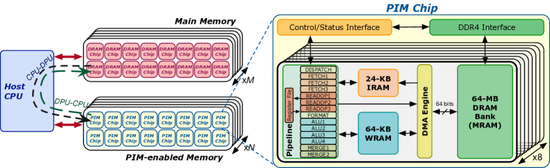
The UPMEM company has designed and fabricated the first commercially-available PIM architecture. The UPMEM PIM architecture [154, 155, 1, 157, 158] combines traditional DRAM memory arrays with general-purpose in-order cores, called DRAM Processing Units (DPUs), integrated in the same DRAM chip. UPMEM PIM chips are mounted on DDR4 memory modules that coexist with regular DRAM modules (i.e., the main memory) attached to a host CPU. Figure 1 (left) depicts a UPMEM-based PIM system with (1) a host CPU, (2) main memory (DRAM memory modules), and (3) PIM-enabled memory (UPMEM modules). PIM-enabled memory can reside on one or more memory channels.
Inside each UPMEM PIM chip (Figure 1 (right)), there are 8 DPUs. Each DPU has exclusive access to (1) a 64-MB DRAM bank, called Main RAM (MRAM), (2) a 24-KB instruction memory, and (3) a 64-KB scratchpad memory, called Working RAM (WRAM). The MRAM banks are accessible by the host CPU for copying input data (from main memory to MRAM) and retrieving results (from MRAM to main memory). These data transfers can be performed in parallel (i.e., concurrently across multiple MRAM banks), if the size of the buffers transferred from/to all MRAM banks is the same. Otherwise, the data transfers happen serially. There is no support for direct communication between DPUs. All inter-DPU communication takes place through the host CPU by retrieving results and copying data.
Rigorously understanding the UPMEM PIM architecture, the first publicly-available PIM architecture, and its suitability to various workloads can provide valuable insights to programmers, users and architects of this architecture as well as of future PIM systems. To this end, our work [1, 157] provides the first comprehensive analysis of the first publicly-available real-world PIM architecture. We make two key contributions. First, we conduct an experimental characterization of the UPMEM-based PIM system using microbenchmarks to assess various architecture limits such as compute throughput and memory bandwidth, yielding new insights. Second, we present PrIM (Processing-In-Memory benchmarks), an open-source benchmark suite [156] of 16 workloads from different application domains (e.g., neural networks, databases, graph processing, bioinformatics), which we identify as memory-bound workloads using the roofline model [159] (i.e., these workloads’ performance in conventional processor-centric architectures is limited by memory access). Table I shows a summary of PrIM benchmarks, including workload characteristics (memory access pattern, computation pattern, communication/synchronization needs) that demonstrate the diversity of the benchmarks.
Our comprehensive analysis [1, 157] evaluates the performance and scaling characteristics of PrIM benchmarks on the UPMEM PIM architecture, and compares their performance and energy consumption to their CPU and GPU counterparts. Our extensive evaluation conducted on two real UPMEM-based PIM systems with 640 and 2,556 DPUs provides new insights about suitability of different workloads to the PIM system, programming recommendations for software designers, and suggestions and hints for hardware and architecture designers of future PIM systems.
In this paper, we provide four key takeaways that represent the main insights and conclusions of our work [1, 157]. For more information about our thorough PIM architecture characterization, methodology, results, insights, and the PrIM benchmark suite, we refer the reader to the full version of the paper [1, 157]. We hope that our study can guide programmers on how to optimize software for real PIM systems and enlighten designers about how to improve the architecture and hardware of future PIM systems. Our microbenchmarks and PrIM benchmark suite are publicly available [156].
II Key Takeaways
We present several key empirical observations in the form of four key takeaways that we distill from our experimental characterization of the UPMEM PIM architecture [1]. We also provide analyses of workload suitability and good programming practices for the UPMEM PIM architecture, and suggestions for hardware and architecture designers of future PIM systems.
Key Takeaway #1. The UPMEM PIM architecture is fundamentally compute bound. Our microbenchmark-based analysis shows that workloads with more complex operations than integer addition fully utilize the instruction pipeline before they can potentially saturate the memory bandwidth. As Figure 2 shows, even workloads with as simple operations as integer addition saturate the compute throughput with an operational intensity as low as 0.25 operations/byte (1 addition per integer accessed).
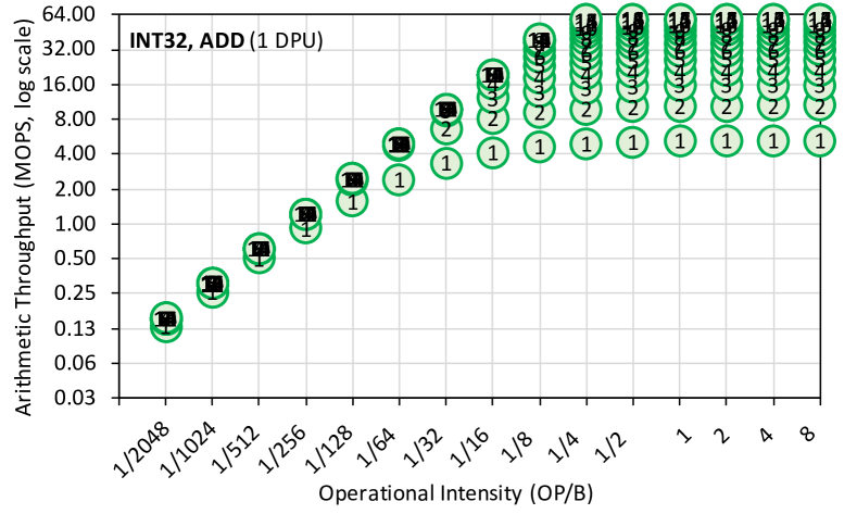
This key takeaway shows that the most suitable workloads for the UPMEM PIM architecture are memory-bound workloads. From a programmer’s perspective, the architecture requires a shift in how we think about computation and data access, since the relative cost of computation vs. data access in the PIM system is very different from that in the dominant processor-centric architectures of today.
Key Takeaway #2. The workloads most well-suited for the UPMEM PIM architecture are those with simple or no arithmetic operations. This is because DPUs include native support for only integer addition/subtraction and bitwise operations. More complex integer (e.g., multiplication, division) and floating point operations are implemented using software library routines. As Figure 3 shows, the arithmetic throughput of more complex integer operations and floating point operations are an order of magnitude lower than that of simple addition and subtraction.
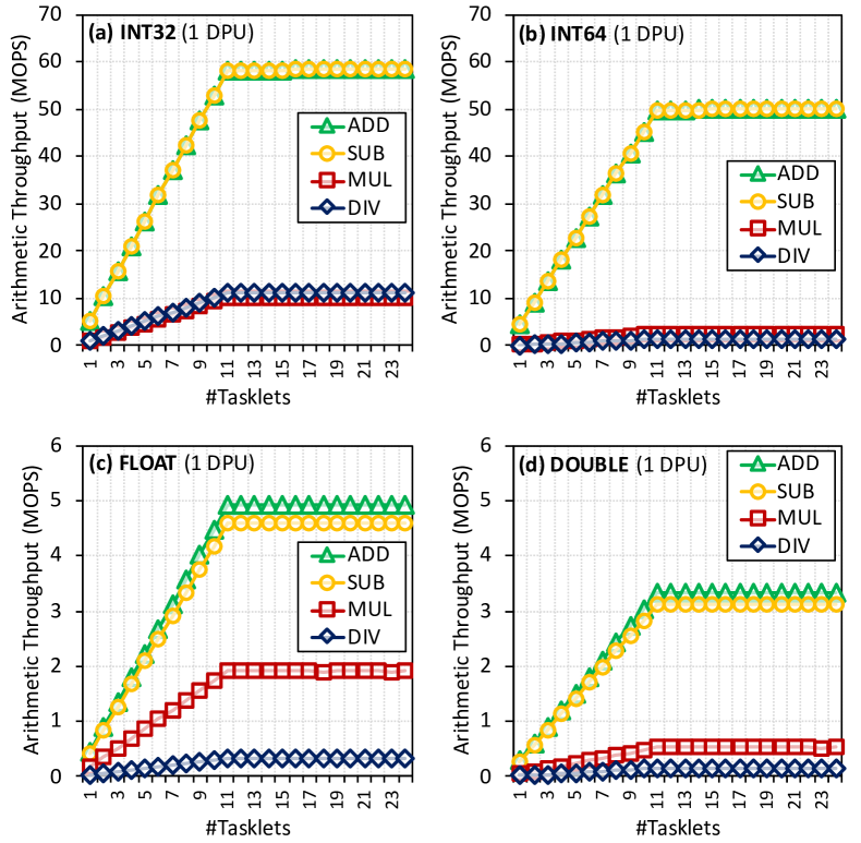
Figure 4 shows the speedup of the UPMEM-based PIM systems with 640 and 2,556 DPUs and a state-of-the-art Titan V GPU over a state-of-the-art Intel Xeon CPU.
We observe that benchmarks with little amount of computation and no use of multiplication, division, or floating point operations (10 out of 16 benchmarks) run faster (2.54 on average) on a 2,556-DPU system than on a state-of-the-art NVIDIA Titan V GPU. These observations show that the workloads most well-suited for the UPMEM PIM architecture are those with no arithmetic operations or simple operations (e.g., bitwise operations and integer addition/subtraction). Based on this key takeaway, we recommend devising much more efficient software library routines or, more importantly, specialized and fast in-memory hardware for complex operations in future PIM architecture generations to improve the general-purpose performance of PIM systems.
Key Takeaway #3. The workloads most well-suited for the UPMEM PIM architecture are those with little global communication, because there is no direct communication channel among DPUs (see Figure 1). As a result, there is a huge disparity in performance scalability of benchmarks that do not require inter-DPU communication and benchmarks that do (especially if parallel transfers across MRAM banks cannot be used). This key takeaway shows that the workloads most well-suited for the UPMEM PIM architecture are those with little or no inter-DPU communication. Based on this takeaway, we recommend that the hardware architecture and the software stack be enhanced with support for inter-DPU communication (e.g., by leveraging new in-DRAM data copy techniques [117, 126, 125, 121] and providing better connectivity inside DRAM [121, 125]).
Summary. We find that the workloads most suitable for the UPMEM PIM architecture in its current form are (1) memory-bound workloads with (2) simple or no arithmetic operations and (3) little or no inter-DPU communication.
Key Takeaway #4. We observe that the existing UPMEM-based PIM systems greatly improve energy efficiency and performance over state-of-the-art CPU and GPU systems across many workloads we examine. Figure 4 shows that the 2,556-DPU and the 640-DPU systems are 23.2 and 10.1 faster, respectively, than a state-of-the-art Intel Xeon CPU, averaged across the entire set of 16 PrIM benchmarks. We also observe that the 640-DPU system is 1.64 more energy efficient than the CPU, averaged across the entire set of 16 PrIM benchmarks, and 5.23 more energy efficient for 12 of the PrIM benchmarks.
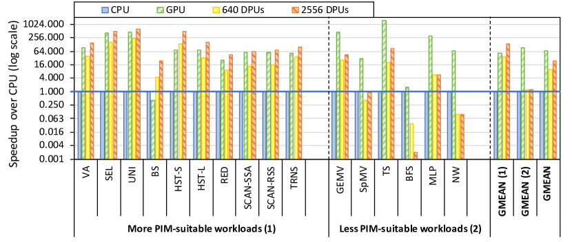
The 2,556-DPU system is faster (on average by 2.54) than the state-of-the-art GPU in 10 out of 16 PrIM benchmarks, which have three key characteristics that define a workload’s PIM suitability: (1) streaming memory accesses, (2) little or no inter-DPU communication, and (3) little or no use of multiplication, division, or floating point operations.
We expect that the 2,556-DPU system will provide even higher performance and energy benefits, and that future PIM systems will be even better (especially after implementing our recommendations for future PIM hardware [1]). If the architecture is improved based on our recommendations under Key Takeaways 1-3 and in [1], we believe future PIM systems will be even more attractive, leading to much higher performance and energy benefits versus state-of-the-art CPUs and GPUs over potentially all workloads.
III Summary & Conclusion
This invited short paper summarizes the first comprehensive characterization and analysis of a real commercial PIM architecture [1, 157]. Through this analysis, we develop a rigorous, thorough understanding of the UPMEM PIM architecture, the first publicly-available PIM architecture, and its suitability to various types of workloads.
First, we conduct a characterization of the UPMEM-based PIM system using microbenchmarks to assess various architecture limits such as compute throughput and memory bandwidth, yielding new insights. Second, we present PrIM, an open-source benchmark suite [156] of 16 memory-bound workloads from different application domains (e.g., dense/sparse linear algebra, databases, data analytics, graph processing, neural networks, bioinformatics, image processing).
Our extensive evaluation of PrIM benchmarks conducted on two real systems with UPMEM memory modules provides new insights about suitability of different workloads to the PIM system, programming recommendations for software designers, and suggestions and hints for hardware and architecture designers of future PIM systems. We compare the performance and energy consumption of the UPMEM-based PIM systems for PrIM benchmarks to those of a state-of-the-art CPU and a state-of-the-art GPU, and identify key workload characteristics that can successfully leverage the strengths of a real PIM system over conventional processor-centric architectures, leading to significant performance and energy improvements.
We believe and hope that our work will provide valuable insights to programmers, users and architects of this PIM architecture as well as of future PIM systems, and will represent an enabling milestone in the development of fundamentally-efficient memory-centric computing systems.
Acknowledgment
We thank UPMEM’s Fabrice Devaux, Rémy Cimadomo, Romaric Jodin, and Vincent Palatin for their valuable support. We acknowledge the support of SAFARI Research Group’s industrial partners, especially ASML, Facebook, Google, Huawei, Intel, Microsoft, VMware, and the Semiconductor Research Corporation. This research was partially supported by the ETH Future Computing Laboratory. Izzat El Hajj acknowledges the support of the University Research Board of the American University of Beirut (URB-AUB-103951-25960). This paper provides a short summary of our larger paper on arxiv.org [1], which has comprehensive descriptions and extensive analyses.
References
- [1] J. Gómez-Luna et al., “Benchmarking a New Paradigm: An Experimental Analysis of a Real Processing-in-Memory Architecture,” arXiv:2105.03814 [cs.AR], 2021.
- [2] O. Mutlu et al., “Processing Data Where It Makes Sense: Enabling In-Memory Computation,” MicPro, 2019.
- [3] O. Mutlu et al., “A Modern Primer on Processing in Memory,” Emerging Computing: From Devices to Systems - Looking Beyond Moore and Von Neumann, 2021, https://arxiv.org/pdf/2012.03112.pdf.
- [4] S. Ghose et al., “Processing-in-Memory: A Workload-Driven Perspective,” IBM JRD, 2019.
- [5] O. Mutlu et al., “Enabling Practical Processing in and near Memory for Data-Intensive Computing,” in DAC, 2019.
- [6] O. Mutlu, “Intelligent Architectures for Intelligent Computing Systems,” in DATE, 2021.
- [7] A. Boroumand et al., “Google Workloads for Consumer Devices: Mitigating Data Movement Bottlenecks,” in ASPLOS, 2018.
- [8] D. Pandiyan and C.-J. Wu, “Quantifying the Energy Cost of Data Movement for Emerging Smart Phone Workloads on Mobile Platforms,” in IISWC, 2014.
- [9] G. Kestor et al., “Quantifying the Energy Cost of Data Movement in Scientific Applications,” in IISWC, 2013.
- [10] W. H. Kautz, “Cellular Logic-in-Memory Arrays,” IEEE TC, 1969.
- [11] H. S. Stone, “A Logic-in-Memory Computer,” IEEE TC, 1970.
- [12] Hybrid Memory Cube Consortium, “HMC Specification 2.0,” 2014.
- [13] JEDEC, “High Bandwidth Memory (HBM) DRAM,” Standard No. JESD235, 2013.
- [14] D. Lee et al., “Simultaneous Multi-Layer Access: Improving 3D-Stacked Memory Bandwidth at Low Cost,” TACO, 2016.
- [15] S. Ghose et al., “Demystifying Complex Workload-DRAM Interactions: An Experimental Study,” in SIGMETRICS, 2019.
- [16] Y. Kim et al., “Ramulator: A Fast and Extensible DRAM Simulator,” CAL, 2015.
- [17] J. Ahn et al., “A Scalable Processing-in-Memory Accelerator for Parallel Graph Processing,” in ISCA, 2015.
- [18] M. Gokhale et al., “Hybrid Memory Cube Performance Characterization on Data-Centric Workloads,” in IA3, 2015.
- [19] B. C. Lee et al., “Architecting Phase Change Memory as a Scalable DRAM Alternative,” in ISCA, 2009.
- [20] E. Kültürsay et al., “Evaluating STT-RAM as an Energy-Efficient Main Memory Alternative,” in ISPASS, 2013.
- [21] D. B. Strukov et al., “The Missing Memristor Found,” Nature, 2008.
- [22] H.-S. P. Wong et al., “Metal-Oxide RRAM,” Proc. IEEE, 2012.
- [23] B. C. Lee et al., “Phase Change Memory Architecture and the Quest for Scalability,” CACM, 2010.
- [24] M. K. Qureshi et al., “Scalable High Performance Main Memory System Using Phase-Change Memory Technology,” in ISCA, 2009.
- [25] P. Zhou et al., “A Durable and Energy Efficient Main Memory Using Phase Change Memory Technology,” in ISCA, 2009.
- [26] B. C. Lee et al., “Phase-Change Technology and the Future of Main Memory,” IEEE Micro, 2010.
- [27] H.-S. P. Wong et al., “Phase Change Memory,” Proc. IEEE, 2010.
- [28] H. Yoon et al., “Efficient Data Mapping and Buffering Techniques for Multilevel Cell Phase-Change Memories,” ACM TACO, 2014.
- [29] H. Yoon et al., “Row Buffer Locality Aware Caching Policies for Hybrid Memories,” in ICCD, 2012.
- [30] P. Girard et al., “A Survey of Test and Reliability Solutions for Magnetic Random Access Memories,” Proceedings of the IEEE, 2020.
- [31] U. Kang et al., “Co-Architecting Controllers and DRAM to Enhance DRAM Process Scaling,” in The Memory Forum, 2014.
- [32] J. Liu et al., “An Experimental Study of Data Retention Behavior in Modern DRAM Devices: Implications for Retention Time Profiling Mechanisms,” in ISCA, 2013.
- [33] O. Mutlu, “Memory Scaling: A Systems Architecture Perspective,” IMW, 2013.
- [34] Y. Kim et al., “Flipping Bits in Memory Without Accessing Them: An Experimental Study of DRAM Disturbance Errors,” in ISCA, 2014.
- [35] O. Mutlu, “The RowHammer Problem and Other Issues We May Face as Memory Becomes Denser,” in DATE, 2017.
- [36] S. Ghose et al., “What Your DRAM Power Models Are Not Telling You: Lessons from a Detailed Experimental Study,” in SIGMETRICS, 2018.
- [37] O. Mutlu and L. Subramanian, “Research Problems and Opportunities in Memory Systems,” SUPERFRI, 2014.
- [38] J. S. Kim et al., “Revisiting RowHammer: An Experimental Analysis of Modern DRAM Devices and Mitigation Techniques,” in ISCA, 2020.
- [39] O. Mutlu and J. S. Kim, “RowHammer: A Retrospective,” IEEE TCAD, 2019.
- [40] P. Frigo et al., “TRRespass: Exploiting the Many Sides of Target Row Refresh,” in S&P, 2020.
- [41] J. Kim et al., “Solar-DRAM: Reducing DRAM Access Latency by Exploiting the Variation in Local Bitlines,” in ICCD, 2018.
- [42] J. Liu et al., “RAIDR: Retention-Aware Intelligent DRAM Refresh,” in ISCA, 2012.
- [43] O. Mutlu, “Main Memory Scaling: Challenges and Solution Directions,” in More than Moore Technologies for Next Generation Computer Design. Springer, 2015.
- [44] J. A. Mandelman et al., “Challenges and Future Directions for the Scaling of Dynamic Random-Access Memory (DRAM),” IBM JRD, 2002.
- [45] L. Cojocar et al., “Are We Susceptible to Rowhammer? An End-to-End Methodology for Cloud Providers,” in S&P, 2020.
- [46] A. G. Yağlikçi et al., “BlockHammer: Preventing RowHammer at Low Cost by Blacklisting Rapidly-Accessed DRAM Rows,” in HPCA, 2021.
- [47] M. Patel et al., “The Reach Profiler (REAPER): Enabling the Mitigation of DRAM Retention Failures via Profiling at Aggressive Conditions,” in ISCA, 2017.
- [48] S. Khan et al., “The Efficacy of Error Mitigation Techniques for DRAM Retention Failures: A Comparative Experimental Study,” in SIGMETRICS, 2014.
- [49] S. Khan et al., “PARBOR: An Efficient System-Level Technique to Detect Data Dependent Failures in DRAM,” in DSN, 2016.
- [50] S. Khan et al., “Detecting and Mitigating Data-Dependent DRAM Failures by Exploiting Current Memory Content,” in MICRO, 2017.
- [51] D. Lee et al., “Adaptive-Latency DRAM: Optimizing DRAM Timing for the Common-Case,” in HPCA, 2015.
- [52] D. Lee et al., “Design-Induced Latency Variation in Modern DRAM Chips: Characterization, Analysis, and Latency Reduction Mechanisms,” in SIGMETRICS, 2017.
- [53] K. K. Chang et al., “Understanding Reduced-Voltage Operation in Modern DRAM Devices: Experimental Characterization, Analysis, and Mechanisms,” in SIGMETRICS, 2017.
- [54] K. K. Chang et al., “Understanding Latency Variation in Modern DRAM Chips: Experimental Characterization, Analysis, and Optimization,” in SIGMETRICS, 2016.
- [55] K. K. Chang et al., “Improving DRAM Performance by Parallelizing Refreshes with Accesses,” in HPCA, 2014.
- [56] J. Meza et al., “Revisiting Memory Errors in Large-Scale Production Data Centers: Analysis and Modeling of New Trends from the Field,” in DSN, 2015.
- [57] H. David et al., “Memory Power Management via Dynamic Voltage/Frequency Scaling,” in ICAC, 2011.
- [58] Q. Deng et al., “Memscale: Active Low-power Modes for Main Memory,” in ASPLOS, 2011.
- [59] S. Hong, “Memory Technology Trend and Future Challenges,” in IEDM, 2010.
- [60] S. Kanev et al., “Profiling a Warehouse-Scale Computer,” in ISCA, 2015.
- [61] M. K. Qureshi et al., “AVATAR: A Variable-Retention-Time (VRT) Aware Refresh for DRAM Systems,” in DSN, 2015.
- [62] L. Orosa et al., “A Deeper Look into RowHammer’s Sensitivities: Experimental Analysis of Real DRAM Chips and Implications on Future Attacks and Defenses,” in MICRO, 2021.
- [63] H. Hassan et al., “Uncovering In-DRAM RowHammer Protection Mechanisms: A New Methodology, Custom RowHammer Patterns, and Implications,” in MICRO, 2021.
- [64] C. Giannoula, “Efficient Synchronization Support for Near-Data-Processing Architectures,” https://people.inf.ethz.ch/omutlu/pub/SynCron-synchronization-for-near-data-processing-systems_hpca21-talk.pptx, video available at https://youtu.be/TV3Xgh3l9do, 2021, SAFARI Live Seminar, 27 September 2021.
- [65] C. Giannoula et al., “SynCron: Efficient Synchronization Support for Near-Data-Processing Architectures,” in HPCA, 2021.
- [66] D. S. Cali et al., “GenASM: A High-Performance, Low-Power Approximate String Matching Acceleration Framework for Genome Sequence Analysis,” in MICRO, 2020.
- [67] M. Alser et al., “Accelerating Genome Analysis: A Primer on an Ongoing Journey,” IEEE Micro, 2020.
- [68] J. S. Kim et al., “GRIM-Filter: Fast Seed Location Filtering in DNA Read Mapping Using Processing-in-Memory Technologies,” BMC Genomics, 2018.
- [69] J. Ahn et al., “PIM-Enabled Instructions: A Low-Overhead, Locality-Aware Processing-in-Memory Architecture,” in ISCA, 2015.
- [70] A. Boroumand et al., “CoNDA: Efficient Cache Coherence Support for near-Data Accelerators,” in ISCA, 2019.
- [71] A. Boroumand et al., “LazyPIM: An Efficient Cache Coherence Mechanism for Processing-in-Memory,” CAL, 2016.
- [72] G. Singh et al., “NAPEL: Near-memory Computing Application Performance Prediction via Ensemble Learning,” in DAC, 2019.
- [73] K. Hsieh et al., “Transparent Offloading and Mapping (TOM): Enabling Programmer-Transparent Near-Data Processing in GPU Systems,” in ISCA, 2016.
- [74] D. Kim et al., “Neurocube: A Programmable Digital Neuromorphic Architecture with High-Density 3D Memory,” in ISCA, 2016.
- [75] G. Kim et al., “Toward Standardized Near-Data Processing with Unrestricted Data Placement for GPUs,” in SC, 2017.
- [76] Z. Liu et al., “Concurrent Data Structures for Near-Memory Computing,” in SPAA, 2017.
- [77] L. Nai et al., “GraphPIM: Enabling Instruction-Level PIM Offloading in Graph Computing Frameworks,” in HPCA, 2017.
- [78] A. Pattnaik et al., “Scheduling Techniques for GPU Architectures with Processing-in-Memory Capabilities,” in PACT, 2016.
- [79] S. H. Pugsley et al., “NDC: Analyzing the Impact of 3D-Stacked Memory+Logic Devices on MapReduce Workloads,” in ISPASS, 2014.
- [80] D. P. Zhang et al., “TOP-PIM: Throughput-Oriented Programmable Processing in Memory,” in HPDC, 2014.
- [81] B. Akin et al., “Data Reorganization in Memory Using 3D-Stacked DRAM,” in ISCA, 2015.
- [82] M. Gao et al., “Tetris: Scalable and Efficient Neural Network Acceleration with 3D Memory,” in ASPLOS, 2017.
- [83] M. Drumond et al., “The Mondrian Data Engine,” in ISCA, 2017.
- [84] G. Dai et al., “GraphH: A Processing-in-Memory Architecture for Large-scale Graph Processing,” IEEE TCAD, 2018.
- [85] M. Zhang et al., “GraphP: Reducing Communication for PIM-based Graph Processing with Efficient Data Partition,” in HPCA, 2018.
- [86] Y. Huang et al., “A Heterogeneous PIM Hardware-Software Co-Design for Energy-Efficient Graph Processing,” in IPDPS, 2020.
- [87] Y. Zhuo et al., “GraphQ: Scalable PIM-based Graph Processing,” in MICRO, 2019.
- [88] A. Boroumand et al., “Polynesia: Enabling Effective Hybrid Transactional/Analytical Databases with Specialized Hardware/Software Co-Design,” arXiv:2103.00798 [cs.AR], 2021.
- [89] S. Lloyd and M. Gokhale, “In-memory Data Rearrangement for Irregular, Data-intensive Computing,” Computer, 2015.
- [90] S. Lloyd and M. Gokhale, “Design Space Exploration of Near Memory Accelerators,” in MEMSYS, 2018.
- [91] M. Gokhale et al., “Near Memory Data Structure Rearrangement,” in MEMSYS, 2015.
- [92] R. Nair et al., “Active Memory Cube: A Processing-in-Memory Architecture for Exascale Systems,” IBM JRD, 2015.
- [93] A. C. Jacob et al., “Compiling for the Active Memory Cube,” Tech. rep. RC25644 (WAT1612-008). IBM Research Division, Tech. Rep., 2016.
- [94] Z. Sura et al., “Data Access Optimization in a Processing-in-Memory System,” in CF, 2015.
- [95] R. Balasubramonian et al., “Near-Data Processing: Insights from a MICRO-46 Workshop,” IEEE Micro, 2014.
- [96] A. Boroumand et al., “Mitigating Edge Machine Learning Inference Bottlenecks: An Empirical Study on Accelerating Google Edge Models,” arXiv:2103.00768 [cs.AR], 2021.
- [97] G. F. Oliveira, “DAMOV: A New Methodology and Benchmark Suite for Evaluating Data Movement Bottlenecks,” https://people.inf.ethz.ch/omutlu/pub/DAMOV-Bottleneck-Analysis-and-DataMovement-Benchmarks_arxiv21-talk.pptx, video available at https://youtu.be/GWideVyo0nM, 2021, SAFARI Live Seminar, 22 July 2021.
- [98] G. F. Oliveira et al., “DAMOV: A New Methodology and Benchmark Suite for Evaluating Data Movement Bottlenecks,” arXiv:2105.03725 [cs.AR], 2021.
- [99] G. F. Oliveira et al., “DAMOV: A New Methodology and Benchmark Suite for Evaluating Data Movement Bottlenecks,” IEEE Access, 2021.
- [100] A. Boroumand et al., “Google Neural Network Models for Edge Devices: Analyzing and Mitigating Machine Learning Inference Bottlenecks,” in PACT, 2021.
- [101] M. Hashemi et al., “Accelerating Dependent Cache Misses with an Enhanced Memory Controller,” in ISCA, 2016.
- [102] M. Hashemi et al., “Continuous Runahead: Transparent Hardware Acceleration for Memory Intensive Workloads,” in MICRO, 2016.
- [103] H. Asghari-Moghaddam et al., “Chameleon: Versatile and Practical Near-DRAM Acceleration Architecture for Large Memory Systems,” in MICRO, 2016.
- [104] M. A. Alves et al., “Opportunities and Challenges of Performing Vector Operations inside the DRAM,” in MEMSYS, 2015.
- [105] W. Huangfu et al., “MEDAL: Scalable DIMM Based Near Data Processing Accelerator for DNA Seeding Algorithm,” in MICRO, 2019.
- [106] I. Fernandez et al., “NATSA: A Near-Data Processing Accelerator for Time Series Analysis,” in ICCD, 2020.
- [107] G. Singh et al., “NERO: A Near High-Bandwidth Memory Stencil Accelerator for Weather Prediction Modeling,” in FPL, 2020.
- [108] G. Singh et al., “FPGA-based Near-Memory Acceleration of Modern Data-Intensive Applications,” IEEE Micro, 2021.
- [109] S. Aga et al., “Compute Caches,” in HPCA, 2017.
- [110] C. Eckert et al., “Neural Cache: Bit-serial In-cache Acceleration of Deep Neural Networks,” in ISCA, 2018.
- [111] D. Fujiki et al., “Duality Cache for Data Parallel Acceleration,” in ISCA, 2019.
- [112] M. Kang et al., “An Energy-Efficient VLSI Architecture for Pattern Recognition via Deep Embedding of Computation in SRAM,” in ICASSP, 2014.
- [113] V. Seshadri and O. Mutlu, “In-DRAM Bulk Bitwise Execution Engine,” arXiv:1905.09822 [cs.AR], 2020.
- [114] V. Seshadri et al., “Fast Bulk Bitwise AND and OR in DRAM,” CAL, 2015.
- [115] V. Seshadri et al., “Ambit: In-Memory Accelerator for Bulk Bitwise Operations Using Commodity DRAM Technology,” in MICRO, 2017.
- [116] V. Seshadri et al., “RowClone: Accelerating Data Movement and Initialization Using DRAM,” arXiv:1805.03502 [cs.AR], 2018.
- [117] V. Seshadri et al., “RowClone: Fast and Energy-Efficient In-DRAM Bulk Data Copy and Initialization,” in MICRO, 2013.
- [118] J. Kim et al., “The DRAM Latency PUF: Quickly Evaluating Physical Unclonable Functions by Exploiting the Latency–Reliability Tradeoff in Modern DRAM Devices,” in HPCA, 2018.
- [119] J. Kim et al., “D-RaNGe: Using Commodity DRAM Devices to Generate True Random Numbers with Low Latency and High Throughput,” in HPCA, 2019.
- [120] F. Gao et al., “ComputeDRAM: In-Memory Compute Using Off-the-Shelf DRAMs,” in MICRO, 2019.
- [121] K. K. Chang et al., “Low-Cost Inter-Linked Subarrays (LISA): Enabling Fast Inter-Subarray Data Movement in DRAM,” in HPCA, 2016.
- [122] S. Li et al., “DRISA: A DRAM-Based Reconfigurable In-Situ Accelerator,” in MICRO, 2017.
- [123] Q. Deng et al., “DrAcc: a DRAM Based Accelerator for Accurate CNN Inference,” in DAC, 2018.
- [124] N. Hajinazar et al., “SIMDRAM: A Framework for Bit-Serial SIMD Processing Using DRAM,” in ASPLOS, 2021.
- [125] S. H. S. Rezaei et al., “NoM: Network-on-Memory for Inter-Bank Data Transfer in Highly-Banked Memories,” CAL, 2020.
- [126] Y. Wang et al., “FIGARO: Improving System Performance via Fine-Grained In-DRAM Data Relocation and Caching,” in MICRO, 2020.
- [127] M. F. Ali et al., “In-Memory Low-Cost Bit-Serial Addition Using Commodity DRAM Technology,” in TCAS-I, 2019.
- [128] J. D. Ferreira et al., “pLUTo: In-DRAM Lookup Tables to Enable Massively Parallel General-Purpose Computation,” arXiv:2104.07699 [cs.AR], 2021.
- [129] A. Olgun et al., “QUAC-TRNG: High-Throughput True Random Number Generation Using Quadruple Row Activation in Commodity DRAMs,” in ISCA, 2021.
- [130] A. Olgun, “QUAC-TRNG: High-Throughput True Random Number Generation Using Quadruple Row Activation in Commodity DRAM Chips,” http://people.inf.ethz.ch/omutlu/pub/QUAC-TRNG-DRAM_isca21-talk.pptx, video available at https://youtu.be/snvF3g3GfkI, 2021, SAFARI Live Seminar, 15 September 2021.
- [131] N. Hajinazar, “Data-Centric and Data-Aware Frameworks for Fundamentally Efficient Data Handling in Modern Computing Systems,” https://arxiv.org/pdf/2109.05881.pdf, video available at https://youtu.be/XIfPHtvA9rw, 2021, SAFARI Live Seminar, 27 October 2021.
- [132] L. Orosa et al., “CODIC: A Low-Cost Substrate for Enabling Custom In-DRAM Functionalities and Optimizations,” in ISCA, 2021.
- [133] S. Li et al., “Pinatubo: A Processing-in-Memory Architecture for Bulk Bitwise Operations in Emerging Non-Volatile Memories,” in DAC, 2016.
- [134] S. Angizi et al., “PIMA-Logic: A Novel Processing-in-Memory Architecture for Highly Flexible and Energy-efficient Logic Computation,” in DAC, 2018.
- [135] S. Angizi et al., “CMP-PIM: An Energy-efficient Comparator-based Processing-in-Memory Neural Network Accelerator,” in DAC, 2018.
- [136] S. Angizi et al., “AlignS: A Processing-in-Memory Accelerator for DNA Short Read Alignment Leveraging SOT-MRAM,” in DAC, 2019.
- [137] Y. Levy et al., “Logic Operations in Memory Using a Memristive Akers Array,” Microelectronics Journal, 2014.
- [138] S. Kvatinsky et al., “MAGIC—Memristor-Aided Logic,” IEEE TCAS II: Express Briefs, 2014.
- [139] A. Shafiee et al., “ISAAC: A Convolutional Neural Network Accelerator with In-situ Analog Arithmetic in Crossbars,” in ISCA, 2016.
- [140] S. Kvatinsky et al., “Memristor-Based IMPLY Logic Design Procedure,” in ICCD, 2011.
- [141] S. Kvatinsky et al., “Memristor-Based Material Implication (IMPLY) Logic: Design Principles and Methodologies,” TVLSI, 2014.
- [142] P.-E. Gaillardon et al., “The Programmable Logic-in-Memory (PLiM) Computer,” in DATE, 2016.
- [143] D. Bhattacharjee et al., “ReVAMP: ReRAM based VLIW Architecture for In-memory Computing,” in DATE, 2017.
- [144] S. Hamdioui et al., “Memristor Based Computation-in-Memory Architecture for Data-intensive Applications,” in DATE, 2015.
- [145] L. Xie et al., “Fast Boolean Logic Papped on Memristor Crossbar,” in ICCD, 2015.
- [146] S. Hamdioui et al., “Memristor for Computing: Myth or Reality?” in DATE, 2017.
- [147] J. Yu et al., “Memristive Devices for Computation-in-Memory,” in DATE, 2018.
- [148] A. Ankit et al., “PUMA: A Programmable Ultra-Efficient Memristor-Based Accelerator for Machine Learning Inference,” in ASPLOS, 2019.
- [149] A. Ankit et al., “PANTHER: A Programmable Architecture for Neural Network Training Harnessing Energy-efficient ReRAM,” IEEE TC, 2020.
- [150] P. Chi et al., “PRIME: A Novel Processing-In-Memory Architecture for Neural Network Computation In ReRAM-Based Main Memory,” in ISCA, 2016.
- [151] L. Song et al., “GraphR: Accelerating Graph Processing using ReRAM,” in HPCA, 2018.
- [152] L. Zheng et al., “RRAM-based TCAMs for pattern search,” in ISCAS, 2016.
- [153] Y. Xi et al., “In-Memory Learning With Analog Resistive Switching Memory: A Review and Perspective,” Proceedings of the IEEE, 2020.
- [154] UPMEM, “Introduction to UPMEM PIM. Processing-in-memory (PIM) on DRAM Accelerator (White Paper),” 2018.
- [155] F. Devaux, “The True Processing In Memory Accelerator,” in Hot Chips, 2019.
- [156] SAFARI Research Group, “PrIM Benchmark Suite,” https://github.com/CMU-SAFARI/prim-benchmarks.
- [157] J. Gómez-Luna, “Understanding a Modern Processing-in-Memory Architecture: Benchmarking and Experimental Characterization,” https://people.inf.ethz.ch/omutlu/pub/PrIM-UPMEM-Tutorial-Analysis-Benchmarking-SAFARI-Live-Seminar-2021-07-12-talk.pptx, video available at https://youtu.be/D8Hjy2iU9l4, 2021, SAFARI Live Seminar, 12 July 2021.
- [158] J. Gómez-Luna, “Lecture 12d: Real Processing-in-DRAM with UPMEM,” https://safari.ethz.ch/architecture/fall2020/lib/exe/fetch.php?media=upmem-2020-10-30.pptx, video available at http://www.youtube.com/watch?v=Sscy1Wrr22A, 2020, Computer Architecture. Fall 2020.
- [159] S. Williams et al., “Roofline: An Insightful Visual Performance Model for Multicore Architectures,” CACM, 2009.