Thru-Hole Epitaxy: Is Remote Epitaxy Really Remote?
Abstract
The remote epitaxy was originally proposed to grow a film, which is not in contact but crystallographically aligned with a substrate and easily detachable due to a van der Waals material as a space layer. Here we show that the claimed remote epitaxy is more likely to be nonremote ‘thru-hole’ epitaxy. On a substrate with thick and symmetrically incompatible van der Waals space layer or even with a three-dimensional amorphous oxide film in-between, we demonstratively grew GaN domains through thru-holes via connectedness-initiated epitaxial lateral overgrowth, not only readily detachable but also crystallographically aligned with a substrate. Our proposed nonremote thru-hole epitaxy, which is embarrassingly straightforward and undemanding, can provide wider applicability of the benefits known to be only available by the claimed remote epitaxy.
Introduction
It is a golden rule that epitaxial growth of a crystalline film is allowed only by direct bonding to a crystalline substrate. Extremely surprising studies reported that a crystalline film was epitaxially grown remotely without direct bonding to an underlying substrate despite an ultrathin defect-free 2D overlayer placed in-between, which was named as remote epitaxy.Kim_Nature_544_340 ; Kong_NM_17_999 ; Jeong_SA_6_eaaz5180 An earlier study, for instance, claimed that GaN can be remotely grown through only up to two layers of graphene but not even a single layer of -BN on underlying GaN.Kong_NM_17_999 This result was explained by the teleported influence of the GaN substrate that was not completely screened.Kong_NM_17_999 Once the thickness of an inserted 2D material becomes above a critical value, the grown film is no longer crystallographically aligned with the underlying substrate.Kong_NM_17_999 ; Jeong_SA_6_eaaz5180
The remote epitaxy strictly requires not only the defect-free growth of 2D material but also the state-of-the-art transfer with precise layer-number control. Nevertheless, great attention has been paid to remote epitaxy since it has been believed to provide the great benefit of easy separation of the film, which is crystallographically aligned with a substrate.Kong_NM_17_999 ; Kim_Nature_544_340 ; Jeong_SA_6_eaaz5180 Several other studies have also demonstrated the facile detachment of a film taken as evidence of remote epitaxy.Jeong_Nanoscale_10_22970 ; Jeong_APL_113_233103 ; Guo_NL_20_33 ; Jeong_ACSANM_3_8920 ; Bae_NM_18_550 Strictly speaking, however, the easy detachability may not necessarily originate from the ‘remoteness’ of the remote epitaxy, but simply indicates that the binding between the film and space layer/substrate is weaker than the adhesion of the film to a detacher such as a thermal release tape. In fact, the entire remoteness of the remote epitaxy across the interface has never been rigorously verified yet. The estimated potential fluctuation across the surface of 2D material/substrate given as theoretical evidence of remote epitaxy was only one-tenth of thermal energy at growth temperature, and more importantly, the corresponding potential profile is essentially uncorrelated to that of the bare substrate.Kong_NM_17_999 Moreover, it turned out that the overlooked connectedness directly to the substrate through the space layer (Extended Data Fig. 7 of Ref. [1]) should not have been neglected. Thus, it is physically more reasonable to presume that the claimed remote epitaxy is not likely to be remote.
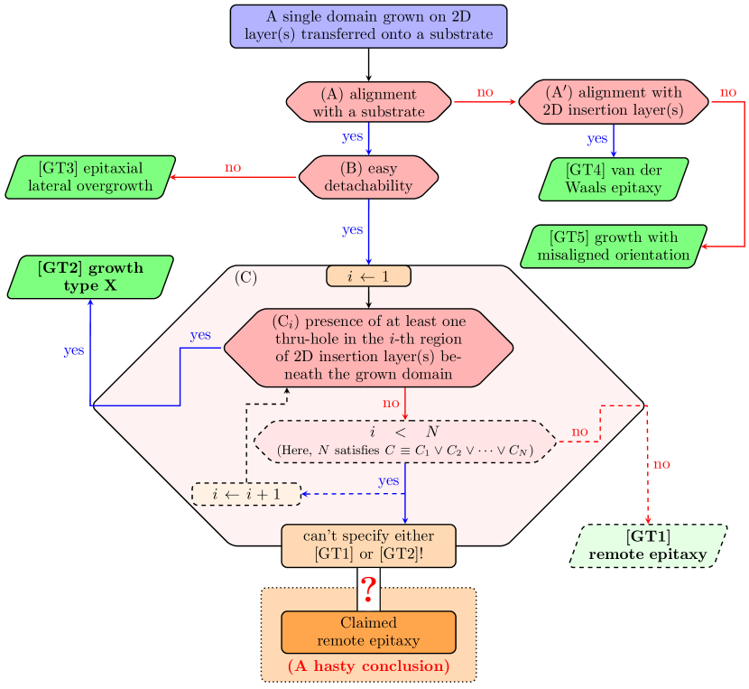
In order to support our argument above, we elaborate on the logic related to growth types categorization. Let us consider a single domain grown on a 2D layer transferred onto a single crystalline substrate. The growth type [GT] for this domain can be categorized into one of the following five as shown in Fig. 1: [GT1] remote epitaxy, [GT2] growth type X, [GT3] epitaxial lateral overgrowth (ELOG), [GT4] van der Waals epitaxy, and [GT5] growth with misaligned orientation. These GT’s were categorized on basis of alignment (A or A′), easy detachability (B), and the existence of at least one thru-hole in the 2D insertion layer beneath the grown domain (C). The presence of at least one thru-hole in the -th region of the 2D insertion layer beneath the growth domain is labeled as (Ci). Thus, (C) is equivalent to where is the number required for the union of 1-st, 2-nd, , -th region to fully cover the entire region of 2D insertion layer beneath the growth domain. On the other hand, the logical negation of (Ci) or NOT (Ci), denoted as , is the complete absence of thru-hole in the -th region of 2D insertion layer beneath the growth domain. Likewise, , indicating NOT (C), is the complete absence of thru-hole in the entire region of 2D insertion layer beneath the growth domain. Of course, these growth types are not necessarily exclusive to one another, and under certain circumstances, mixed growth types may be observed among various domains or within a merged film. However, for the simplicity of discussion, we assume that one growth type is associated with one single domain.
The necessary and sufficient condition for [GT1] remote epitaxy is the combination of (A) and . The verification of requires a full series of high-resolution cross-sectional transmission electron microscopy (HR-TEM) images all across the interface, which has never been given yet. This kind of extensive HR-TEM measurements is, however, impractical even for micro-sized domains, so that the verification of , which was typically shown by a single HR-TEM image in the previous papers on remote epitaxy, was provided as evidence for remote epitaxy instead of . On the other hand, we named any growth type, which satisfies (A), (B), and (C), as [GT2] growth type X, which is definitely not [GT1] remote epitaxy. As can be readily inferred from Fig. 1, however, a connectedness-initiated epitaxy through very small thru-holes can be a candidate for [GT2] growth type X because HR-TEM in the thru-hole-free region of the domain grown by [GT2] growth type X can reveal that is satisfied and only a few small thru-holes may allow easy detachability. In our manuscript, the existence of growth type X was explicitly verified and we identified this growth type X as thru-hole epitaxy. [GT2] Thru-hole epitaxy distinctively refers to the case in which grown domains are not only aligned with a substrate but also easily detached. Easy detachability is the main distinction of [GT2] thru-hole epitaxy differentiating from conventional [GT3] ELOG. As can be seen from Fig. 1, we would like to emphasize that the combination of (A), (B) and is not enough to specify either [GT1] remote epitaxy or [GT2] growth type X, i.e., thru-hole epitaxy. In other words, the combination of (A), (B) and is not sufficient enough to verify the existence of [GT1] remote epitaxy. Note that remote epitaxy was claimed as a growth type in a farfetched manner on basis of insufficient experimental evidence by which [GT1] or [GT2] cannot be specified.
Furthermore, we show that all the other claimed evidences of remote epitaxy are also evidences of thru-hole epitaxy. (See Supplementary Note1 for more detailed explanation.) Thus, either remote epitaxy or thru-hole epitaxy cannot be specified on basis of all the combined experimental evidences, claimed by remote epitaxy, which are just necessary conditions of remote epitaxy. Only if equivalent to were verified, the existence of [GT1] remote epitaxy would be verified. The flaw of logic in the previous papers on remote epitaxy is that the existence of [GT1] remote epitaxy was claimed to be confirmed only by instead of although other evidences were given. Moreover, our computational simulation revealed that the theoretical evidence of [GT1] remote epitaxy is questionable as described below. With appropriate justification ((i) logic flow chart, (ii) our experimental results, and (iii) our computational simulation), we claim that the existence of remote epitaxy has not been verified yet and is questionable.
It appears that the original proposers of remote epitaxy recently realized the existence of thru-holes and recognized that the previous experimental evidences for remote epitaxy may not be enough to specify either [GT1] remote epitaxy or [GT2] thru-hole epitaxy.Kim_ACSNano_15_10587 In order to find out the role of thru-holes and specify either remote epitaxy or thru-hole epitaxy, they designed and carried out experiments, but they reached a hasty conclusion in which [GT2] was excluded even in the presence of thru-holes.Kim_ACSNano_15_10587 (See Supplementary Note2 for the more detailed explanation.)
Results and discussion
Based on the argument made above, we hypothesized that the claimed remote epitaxy may simply be ‘thru-hole’ epitaxy composed of two processes through nanoscale holes sparsely distributed in the space layer: nucleation on the exposed substrate and lateral growthNam_APL_71_2638 over the space layer. To verify our proposed hypothesis, we demonstratively grew epitaxial GaN domains under various et mediocri conditions, which are far from those required by the state-of-the-art growth and transfer indispensable in the claimed remote epitaxy. By doing so, we reveal that our proposed nonremote thru-hole epitaxy can equally well provide in an unprecedentedly straightforward manner the benefits, which are supposedly accompanied only by the claimed remote epitaxy, such as facile detachability and crystallographic alignment with a substrate. In the following, we first provide computational results showing the unfeasibility of remote epitaxy and then experimental results verifying thru-hole epitaxy.
Computational evidence questioning remote epitaxy
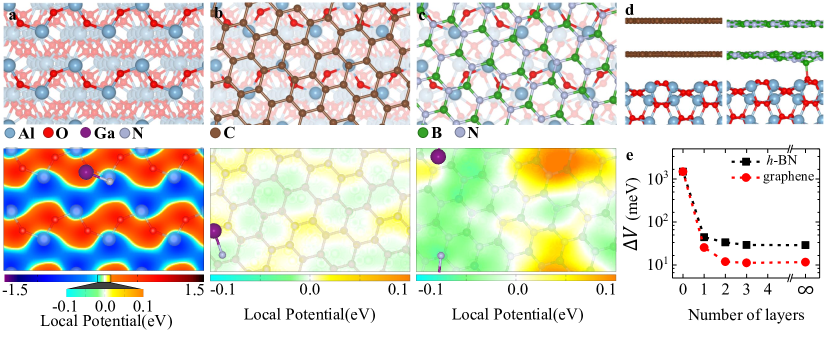
The remote epitaxy proposed by earlier studiesKong_NM_17_999 ; Kim_Nature_544_340 ; Jeong_SA_6_eaaz5180 ; Jeong_Nanoscale_10_22970 ; Jeong_APL_113_233103 ; Guo_NL_20_33 ; Jeong_ACSANM_3_8920 ; Bae_NM_18_550 was validated mainly by the surface potential distribution calculated over a space layer complying with that of a substrate. We discussed some questions raised from the previous calculations in Supplementary Note3. To verify whether such validation is indeed valid, we evaluated the electrostatic potential distributions on various surfaces including not only bare substrates such as sapphire, Si, GaAs, GaN, and LiF but also those substrates with a 2D graphene or -BN overlayer, which will later be denoted as ‘overlayer/substrate’, using the first-principles density functional theory (DFT) calculations. As an exemplary demonstration, we display the surface structures of the bare -sapphire, graphene/-sapphire, and -BN/-sapphire in the top view and their calculated surface potential profiles in Figs. 2(a–c), respectively. Here we emphasize that a computationally-convenient small commensurate stacking configuration introduced to resolve the lattice mismatch between the substrate and the 2D overlayer instigates an artificially periodic potential fluctuation, which would lead to a misinterpretation, as discussed later. To mimic a naturally-occurring incommensurate stacking, we thus constructed relatively a large supercell structure composed of 2D overlayer/-sapphire.
As shown in the lower part of Fig. 2a, the bare -sapphire without a space layer generates a huge potential variation, which is attributed to both a strong ionic characteristic of Al-O bonds and an uneven surface configuration of the substrate. When a monolayer () of the 2D space overlayer, either graphene or -BN, covers the -sapphire, not only is the surface potential variation drastically reduced due to the screening of the space layer, but it does not reflect the shape of the potential profile on the -sapphire substrate, as shown in the lower parts of Figs. 2b and c. With one more layer () of the overlayer material, not to mention the complete dissimilarity between its surface potential distribution and that on the bare substrate, the surface potential variation becomes much smaller, being almost close to that over the overlayer itself without the substrate, since the second layer is essentially flat as shown in Fig. 2d. Furthermore, the potential variations for cases were found to be almost the same as that of either isolated graphene or -BN, as shown in Supplementary Fig. 1.
To examine whether the remote epitaxy would indeed have been eventuated on defect-free 2D space materials, we estimated the potential difference undergone by a Ga-N dimer regarded as a primordial growth seed that should anchor on the 2D overlayer with a similar orientation to on the bare substrate to guarantee the remote epitaxy. Figure. 2e shows as a function of the layer numbers of 2D graphene and -BN overlayers. Even with , was calculated to be only % of that on the bare sapphire, and rapidly converged to the value on the 2D overlayer without the substrate when . For comparison, over other substrates, such as Si, GaAs, GaN, and LiF, we evaluated their potential variations at Å, near which the 2D space layer would locate, above their surfaces, to know over which substrate the potential variations emerge through a 2D space layer. As shown in Supplementary Fig. 2, the magnitude of the evaluated potential variation only over the GaN substrate is similar to that over the -sapphire, but those over the other substrates are much smaller. Thus, the teleportation of substrate potential variations through a 2D space layer is not likely to occur over any kind of substrates as seen in Fig. 2 for -sapphire.
We further investigated the potential variations on the - and -sapphire substrates while increasing the layer number of the -BN space material from to , whose trends are essentially identical to that on the -sapphire case, as shown in Supplementary Fig. 3. To verify the effect of an artificially-generated periodicity caused by the strain applied to forcibly match the lattice mismatch between the substrate and the space layer as mentioned above, we evaluated the surface potential profiles over various stacking configurations of -BN/-sapphire, the combination of which clearly evinces such stacking effect. As displayed in Supplementary Fig. 4, the calculated potential variations are very sensitive to a choice of stacking configurations. Especially, in small supercell configurations, local potential variations look as if that of the substrate would be reflected over the 2D space layer, but this is a misleading artifact caused by such a forcibly matched stacking to make it commensurate. Therefore, the potential fluctuation of 2D material/substrate does not truly reflect the orientation and periodicity of the underlying substrate if the artifact originating from artificial stacking configurations is simply excluded. For a detailed explanation, see Supplementary Note4.
Based on our calculations, the remoteness of the claimed remote epitaxyKong_NM_17_999 ; Kim_Nature_544_340 ; Jeong_SA_6_eaaz5180 ; Jeong_Nanoscale_10_22970 ; Jeong_APL_113_233103 ; Guo_NL_20_33 ; Jeong_ACSANM_3_8920 ; Bae_NM_18_550 is conceptually and strongly questionable, and thus it should be replaced by a genuine growth mechanism, nonremote thru-hole epitaxy. The proposed thru-hole epitaxy enabled us to grow epitaxial GaN domains, which still exhibit all the benefits from the seemingly remote epitaxy, in the growth regime even prohibited by the claimed remote epitaxy.
Thru-hole epitaxy enabled by connectedness
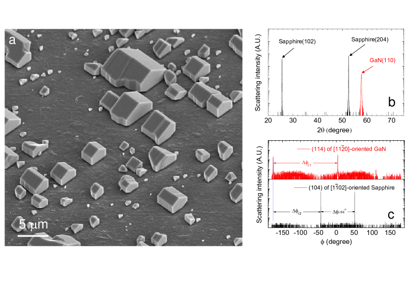
To verify our proposed growth mechanism, we grew GaN domains on a thick and polycrystalline -BN space layer transferred onto -, - and -oriented sapphire substrates. The thickness of -BN was deliberately chosen by multiple transfers to make the influence of a substrate completely negligible and to entirely exclude the remoteness of the claimed remote epitaxy. It was surprisingly observed that those GaN domains grown on a -BN/-sapphire substrate exhibit the [112̄0]-orientation with a garble-roof-shape as if directly grown on the bare -sapphire substrate, as shown in a secondary electron image (SEI) of Fig. 3a. Even more surprisingly, those [112̄0]-oriented GaN domains were all in-plane aligned with one another on the thick and randomly-oriented polycrystalline -BN layer, (Supplementary Fig. 5) clearly indicating that the growth result is not what is expected in van der Waals epitaxy but exactly what would be expected in the claimed remote epitaxy. The crystallographic alignment of those GaN domains with the -sapphire substrate is confirmed by X-ray scattering measurement as shown in Figs. 3b and c. Likewise, similar results were observed on -BN/- and -sapphire. (Supplementary Fig. 6) We observed the exact one-to-one correspondence in Bragg peaks of GaN domains respectively grown on -BN/sapphire and on bare sapphire. (Supplementary Fig. 7) It seemed that we dramatically extended the applicable growth regime of the claimed remote epitaxy, resulting from the crystallographic information of sapphire teleported to GaN even across a thick -BN space layer.
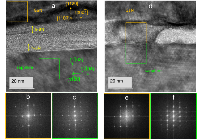
Then, what caused this astonishing crystallographic alignment of GaN domains with underlying sapphire substrates even covered by the thick and polycrystalline -BN? To answer this question, we extensively performed TEM measurement. Figure 4a shows a high-resolution cross-sectional TEM image revealing the interfacial region of GaN and -sapphire with a thick -BN space layer in-between. (Supplementary Fig. 8) Enigmatically, the fast Fourier transformation (FFT) analysis shown in Figs. 4b and c revealed that GaN, which is [112̄0]-oriented, right above thick -BN was aligned with -sapphire consistent with XRD measurements shown in Figs. 3b and c. It was unveiled that the origin of this striking crystallographic alignment of GaN is thru-hole epitaxy. As shown in Fig. 4d, [112̄0]-oriented GaN was directly connected to the -sapphire substrate through thru-holes in -BN in spite of multiple transfers of -BN. (Supplementary Fig. 9) As shown in Fig. 4e and f, FFTs near thru-holes through which GaN and sapphire are connected show the crystallographic alignment of GaN with underlying sapphire. It can be naturally inferred that GaN nucleated on exposed sapphire through thru-holes must have laterally grown over a thick -BN space layer as seen in Fig. 4a. Our experimental results, absolutely unexpected by the claimed remote epitaxy, were made possible not because the remoteness was mysteriously enhanced but because the connectedness was securely established.
It is the first direct evidence of our proposed thru-hole epitaxy, which is applicable to any systems and also even to the claimed remote epitaxy. It is farfetched that the claimed remote epitaxy was attributed to remoteness, but it is rather reasonable to connectedness secured by thru-hole epitaxy, as verified by our computational results described above. In a previous study, as a matter of fact, this same kind of connectedness was also observed on small areas but unfortunately disregarded as a minor effect.Kim_Nature_544_340 Being above the critical layer thickness or losing the connectedness is the reason why the claimed remote epitaxy fails. Thus, we claim that the connectedness serving as a control parameter is utilized as a true criterion not only for the claimed remote epitaxy but also for the thru-hole epitaxy. We showed how to control the extent of the connectedness by intentionally adjusting the thickness of and deliberately not improving the quality of a 2D space layer. (Supplementary Fig. 10) We emphasize that the better the quality of a 2D space layer the lower the density of thru-holes. As a result, the weaker the connectedness the smaller the critical value of the thickness, above which the claimed remote epitaxy or the thru-hole epitaxy is forbidden.Kong_NM_17_999 ; Jeong_Nanoscale_10_22970 Therefore, the thru-hole epitaxy of crystallographically aligned GaN on -BN/sapphire does not require the state-of-the-art perfection of -BN at all.
The readily facile detachability of a grown film crystallographically aligned with an underlying substrate is the exclusive benefit of the claimed remote epitaxy. To check whether the grown film by thru-hole epitaxy is readily detachable as well, we carried out the detachability experiment. Supplementary Fig. 11 shows that GaN domains were readily detached simply by using a thermal release tape although they were connected to the substrate by thru-holes. (Supplementary Fig. 12) We emphasize that there is a critical connectedness below which all the benefits of the claimed remote epitaxy can be obtainable. Unlike the stringent requirement imposed by the claimed remote epitaxy, the connectedness below such critical connectedness is readily achievable. (Supplementary Fig. 13)
Extended demonstration of thru-hole epitaxy
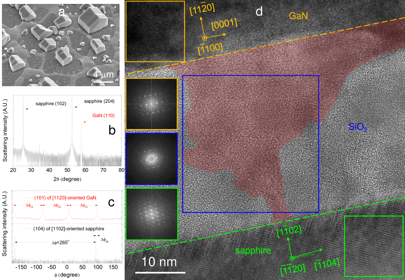
Our experimental results showed that the connectedness by thru-holes is crucial to achieving the crystallographic alignment of a film with a 2D-layer-covered substrate. As long as the connectedness is maintained, the thru-hole epitaxy was found to be valid regardless of either the type or the thickness of a space layer. Our proposed mechanism might, however, be challenged by the speculation that the growth was partly initiated over the -BN regions the thickness of which was less than a critical value of the claimed remote epitaxy. To unambiguously exclude the speculation, we introduced an additional 50-nm-thick SiO2 space layer between -BN and -sapphire to form SiO2/-sapphire with and without -BN overlayer, which should completely suppress the remoteness. Subsequently, nanoscale openings were produced in SiO2 to achieve connectedness. This experimental configuration fully guarantees the thru-hole epitaxy but completely eliminates the possibility of the remote epitaxy. As expected from the thru-hole epitaxy, GaN domains grown in these experimental configurations were crystallographically aligned with -sapphire as shown in Figs. 5(a–c). This result indicates that we successfully achieved the connectedness by intentionally creating nanoscale openings, (See Methods section) verified by TEM analysis as shown in Fig. 5d and Supplementary Fig. 14. The thru-hole epitaxy is robustly manifested even with a SiO2 space layer.
Moreover, we also successfully detached those [112̄0]-oriented GaN domains from -BN/SiO2/-sapphire simply by using a thermal release tape as shown in Supplementary Fig. 15. Here we would like to emphasize that the crystallographic alignment is associated with the connectedness, whereas -BN or any 2D van der Waals space layer plays a role in not transferring the crystallographic information through but only in allowing the film grown above to be readily detachable.
We have shown that ostensibly ‘remote’ epitaxy based on remoteness is evinced by the nonremote thru-hole epitaxy originating from connectedness. Our proposed thru-hole epitaxy mechanism maintains every advantage (e.g., undemanding detachability, crystallographical alignment with an underlying substrate, independence of space layer symmetry) of the remote epitaxy in an embarrassingly straightforward and undemanding manner. It was also demonstrated that our method can be readily extended to hBN/substrate even with a thick SiO2 film in-between without compromising the advantages described above. This growth behavior can open possibilities for the great advantage of detachable heteroepitaxial film growth with no constraint on the state-of-the-art transfer perfection of 2D materials and the thickness of which should be less than a few layers imposed by the claimed remote epitaxy.
References
- (1) Kim, Y. et al. Remote epitaxy through graphene enables two-dimensional material-based layer transfer. Nature 544, 340–343 (2017).
- (2) Kong, W. et al. Polarity governs atomic interaction through two-dimensional materials. Nature Mater. 17, 999–1005 (2018).
- (3) Jeong, J. et al. Remote heteroepitaxy of GaN microrod heterostructures for deformable light-emitting diodes and wafer recycle. Science Advances 6, eaaz5180 (2020).
- (4) Jeong, J. et al. Remote homoepitaxy of ZnO microrods across graphene layers. Nanoscale 10, 22970–22980 (2018).
- (5) Jeong, J. et al. Remote heteroepitaxy across graphene: Hydrothermal growth of vertical ZnO microrods on graphene-coated GaN substrate. Appl. Phys. Lett. 113, 233103 (2018).
- (6) Guo, Y. et al. A Reconfigurable Remotely Epitaxial VO2 Electrical Heterostructure. Nano Lett. 20, 33–42 (2019).
- (7) Jeong, J. et al. Selective-Area Remote Epitaxy of ZnO Microrods Using Multilayer–Monolayer-Patterned Graphene for Transferable and Flexible Device Fabrications. ACS Applied Nano Materials 3, 8920–8930 (2020).
- (8) Bae, S.-H. et al. Integration of bulk materials with two-dimensional materials for physical coupling and applications. Nature Mater. 18, 550–560 (2019).
- (9) Kim, H. et al. Impact of 2D–3D Heterointerface on Remote Epitaxial Interaction through Graphene. ACS Nano 15, 10587–10596 (2021).
- (10) Nam, O. H., Bremser, M. D., Zheleva, T. S. & Davis, R. F. Lateral epitaxy of low defect density GaN layers via organometallic vapor phase epitaxy. Appl. Phys. Lett. 71, 2638–2640 (1997).
- (11) Shin, D. et al. Spontaneous inversion of in-plane polarity of -oriented GaN domains laterally overgrown on patterned -plane sapphire substrates. J. Appl. Cryst. 46, 443–447 (2013).
- (12) Chen, C. et al. A new selective area lateral epitaxial approach for depositing -plane GaN over -plane sapphire. Jpn. J. Appl. Phys. 42, L818–L820 (2003).
- (13) Imer, B., Wu, F., Speck, J. S. & DenBaars, P. Growth evolution in sidewall lateral epitaxial overgrowth (SLEO). J. Crst. Growth 306, 330–338 (2007).
- (14) Jang, D., Jue, M., Yoon, H. & Kim, C. Catalytic decomposition of SiO2 by Fe and the effect of Cu on the behavior of released Si species. Curr. Appl. Phys. 16, 93–100 (2016).
- (15) Kohn, W. & Sham, L. J. Self-Consistent Equations Including Exchange and Correlation Effects. Phys. Rev. 140, A1133–A1138 (1965).
- (16) Kresse, G. & Furthmüller, J. Efficient iterative schemes for ab initio total-energy calculations using a plane-wave basis set. Phys. Rev. B 54, 11169–11186 (1996).
- (17) Blöchl, P. E. Projector augmented-wave method. Phys. Rev. B 50, 17953–17979 (1994).
- (18) Kresse, G. & Joubert, D. From ultrasoft pseudopotentials to the projector augmented-wave method. Phys. Rev. B 59, 1758–1775 (1999).
- (19) Perdew, J. P., Burke, K. & Ernzerhof, M. Generalized Gradient Approximation Made Simple. Phys. Rev. Lett. 77, 3865–3868 (1996).
- (20) Grimme, S. Semiempirical GGA-type density functional constructed with a long-range dispersion correction. J. Comput. Chem. 27, 1787–1799 (2006).
- (21) Monkhorst, H. J. & Pack, J. D. Special points for Brillouin-zone integrations. Phys. Rev. B 13, 5188–5192 (1976).
- (22) Wu, Q. & Yang, W. A direct optimization method for calculating density functionals and exchange-correlation potentials from electron densities. J. Chem. Phys. 118, 2498–2509 (2003).
Methods
- Processes of the thru-hole epitaxy.
-
The thru-hole epitaxy consists of the following processes, growth and transfer of -BN, and growth of GaN, which were carried out with no special optimization. Despite no optimization, we were able to accomplish the thru-hole epitaxy to the extent demanded, indicating that state-of-the-art perfection is not necessary for the thru-hole epitaxy.
- Growth of -BN.
-
A polycrystalline -BN thin film was grown on a Cu foil by chemical vapor deposition (CVD) at 1000∘C with hydrogen (50 sccm) and argon (100 sccm) as a carrier gas as shown in Supplementary Fig. 5. Growth was carried out with ammonia borane (NH3BH3) as a precursor for two hours after two-hour annealing of the Cu foil. The thickness of -BN was roughly estimated to be 2–4 nanometer by transmission electron microscopy. The chemical identification of -BN is shown in Supplementary Fig. 9.
- Transfer of -BN.
-
This CVD-grown -BN was transferred onto -, -, and -sapphire substrates by applying a wet transfer method with poly (methyl methacrylate) (PMMA). PMMA was spin-coated over -BN grown on a Cu foil, which was then etched with FeCl3. PMMA/-BN was transferred onto the desired substrate, and then that was rinsed twice with deionized water. After that, the PMMA was removed by acetone, and -BN/substrate was cleaned by isopropyl alcohol. The extent of the connectedness was intentionally controlled by changing the number of transfers made. For multiple transfers of -BN, the transfer steps listed above were simply repeated.
- Creation of thru-holes in SiO2.
-
We intentionally created the connectedness by introducing thru-holes in a SiO2 space layer. Thru-holes were produced in SiO2 during the pre-heating step of the GaN growth by utilizing FeCl3, which is known to thermally decompose SiO2.Jang_CAP_16_93
- Growth of GaN.
-
GaN was grown on -BN/sapphire or -BN/SiO2/sapphire by using hydride vapor phase epitaxy at 960∘C with HCl (10 sccm) flown over metal Ga and NH3 (1500 sccm) carried by N2.
- Electron microscopy, focused ion beam, and EDS.
-
Transmission electron microscopy (TEM) and selected area diffraction (SAD) measurements were performed by using a Thermo Fisher TitanTM80-300 microscope operated at 300 kV. The available point resolution is better than 1 Å at the operating acceleration voltage. TEM images were recorded by using a charge-coupled camera (Gatan, Oneview095). Scanning TEM (STEM) & energy dispersive spectroscopy (EDS) analysis with Super-X EDS was made by using a Thermo Fisher Talos F200X at 200 kV with a probe size of 1 nm. Secondary electron images (SEIs) were taken by using Hitachi S-4700. For the preparation of TEM samples, focused ion beam (Hitachi, NX5000) was utilized.
- Computational simulation.
-
First-principles calculations were performed using the density functional theoryKohn1965 as implemented in Vienna ab initio simulation package (VASP)Kresse1996 . The electronic wavefunctions were expanded by plane wave basis with a kinetic energy cutoff of 520 eV. We employed the projector-augmented wave pseudopotentialsBlochl1994 ; Kresse1999 to describe the valence electrons, and treated exchange-correlation functional within the generalized gradient approximation of Perdew-Burke-Ernzerhof.Perdew1996 Interlayer interactions were incorporated with Grimme-D2 van der Waals correction.grimme-d2 To reduce long-range interactions from neighboring cells located along the out-of-plane or growth direction, we included a sufficiently large vacuum region of 20 Å. The Brillouin zone (BZ) of each structure was sampled using a separation of 0.04 Å-1 -point mesh according to the Monkhost-Pack scheme.MP The structures were relaxed until all forces became smaller than 0.02 eV/Å. The exchange-correlation potential was excluded in potential fluctuation maps because exchange-correlation potential on a long distance from the surface is incorrect within standard DFT.Kong_NM_17_999 ; LVTOT Various 2D overlayer/sapphire supercell structures were constructed to avoid artificially generated periodic potentials.
Acknowledgments
We gratefully acknowledge financial support from the Korean government (MSIT, MOE) through the National Research Foundation (NRF) of Korea (NRF-2019R1A2C1005417, NRF-2019R1F1A1063643, NRF-2020R1F1A1050725, NRF-2020R1A5A6017701,
NRF-2021R1A5A1032996, BK21 FOUR Program). Some portion of our computational work was done using the resources of the KISTI Supercomputing Center (KSC-2020-CRE-0011).
Author Contributions
Y.L. and S.L. carried out the computational simulation, supervised by Y.-K.K. C.A. performed the growth and transfer of -BN, supervised by J.C. D.J carried out the growth and transfer of GaN with assistance from H.L. and D.K., supervised by C.K. Data analysis and figure preparation of XRD and TEM were performed by D.J. and C.K. The manuscript was written by Y.-K.K., J.C., and C.K. with assistance from all the authors.
Competing interests
The authors declare no competing interests.
Data availability
All data are available in the main text or the supplementary information.
See pages ,- of SI.pdf