HyGain: High Performance, Energy-Efficient Hybrid Gain Cell based Cache Hierarchy
Abstract.
In this paper, we propose a “full-stack” solution to designing high capacity and low latency on-chip cache hierarchies by starting at the circuit level of the hardware design stack. First, we propose a novel Gain Cell (GC) design using FDSOI. The GC has several desirable characteristics, including ~50% higher storage density and ~50% lower dynamic energy as compared to the traditional 6T SRAM, even after accounting for peripheral circuit overheads. We also exploit back-gate bias to increase retention time to 1.12 ms (~60 of eDRAM) which, combined with optimizations like staggered refresh, makes it an ideal candidate to architect all levels of on-chip caches. We show that compared to 6T SRAM, for a given area budget, GC based caches, on average, provide 29% and 36% increase in IPC for single- and multi-programmed workloads, respectively on contemporary workloads including SPEC CPU 2017. We also observe dynamic energy savings of 42% and 34% for single- and multi-programmed workloads, respectively.
We utilize the inherent properties of the proposed GC, including decoupled read and write bitlines to devise optimizations to save precharge energy and architect GC caches with better energy and performance characteristics. Finally, in a quest to utilize the best of all worlds, we combine GC with STT-RAM to create hybrid hierarchies. We show that a hybrid hierarchy with GC caches at L1 and L2, and an LLC split between GC and STT-RAM, with asymmetric write optimization enabled, is able to provide a 54% benefit in energy-delay product (EDP) as compared to an all-SRAM design, and 13% as compared to an all-GC cache hierarchy, averaged across multi-programmed workloads.
1. Introduction
With the (Lamport, 1986) increasing number of cores on-chip (Hsu et al., 2005), additional memory is needed to feed these cores. Emerging workloads have become significantly memory intensive and have large working set sizes (Lin et al., 2009; Singh and Awasthi, 2019). These factors have necessitated the need for high capacity, low latency, on-chip caches.
Several research efforts have been made to increase capacity and contain latency of on-chip caches, which has led to ever-increasing cache capacities and deeper cache hierarchies (Lin et al., 2009). However, the memory technology, which makes up the bulk of on-chip caches, has remained unchanged. On-chip caches, at almost all levels of the memory hierarchy, have been devised using 6T SRAM. Even though SRAM suffers from low areal density, high leakage power and high dynamic energy requirements compared to other memory technologies (Chang et al., 2013; Weste and Harris, 2015; Rabaey et al., 2002), the latency superiority of SRAM, and its compatibility with logic fabrication technology has made it indispensable for creating low-latency caches.
Recently, a number of alternative memory technologies have started to emerge, and have been evaluated for use in caches. Contenders for SRAM replacement include non-volatile memory technologies like Spin-Transfer Torque RAM (STT-RAM) (Xu et al., 2011; Sun et al., 2009; Smullen et al., 2011) and Phase Change Memory (PCM) (Mangalagiri et al., 2008), as well as volatile ones like embedded DRAM (eDRAM) (Chang et al., 2013).
In addition to providing data non-volatility, both STT-RAM and PCM provide 3-4 density benefits over 6T SRAM (Sun et al., 2009; Mangalagiri et al., 2008), making them attractive candidates for high capacity caches. However, there are drawbacks inherent to both technologies, including higher write energy (up to ~5 that of SRAM) and access latencies (~1.5 read, 5 write latency for STT-RAM, PCM is worse) (Sun et al., 2009; Mangalagiri et al., 2008). In most cases, the drawbacks outweigh the benefits, rendering these technologies suitable for use only in last-level caches, where both capacities and access latencies are expected to be higher.
| SRAM | STT-RAM (Jog et al., 2012) | PCM(Mangalagiri et al., 2008) | 1T1C eDRAM(Adkisson et al., 2002) | 2T GC(Somasekhar et al., 2009) | 3T GC (Giterman et al., 2016) | 4T GC (Giterman et al., 2018) | Proposed | |||
| Total Transistors | 6T | 1T+1MTJ | 1T+1PCM | 1T+1C | 2T | 3T | 4T | 2T | ||
| Area (um2) | 0.64 | 0.16 | 0.16 | 0.16 | 0.24 | 0.38 | 0.54 | 0.24 | ||
| Data Storage | Latch | Magnetization | Phase | Capacitor | MOS | MOS | MOS | MOS | ||
| Read/Write Time | Short/Short | Short/Long | Short/Long | Short/Short | Short/Short | Short/Short | Short/Long | Short/Short | ||
| Read/Write Energy | X/Y | X/5Y | X/5Y | 0.5X/0.5Y | 0.5X/0.5Y | 0.5X/0.5Y | 0.5X/0.5Y | 0.5X/0.5Y | ||
| Leakage/Yield | High/High | Low/High | Low/High | Low/Low | Low/High | Low/High | Low/High | Low/High | ||
| Retention Time | - | - | - | 20 us | 20 us | 20 us | 1.6 ms | 1.12 ms | ||
|
No/No | No/Yes | No/Yes | Yes/No | No/Yes | No/Yes | No/Yes | No/Yes |
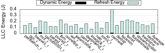
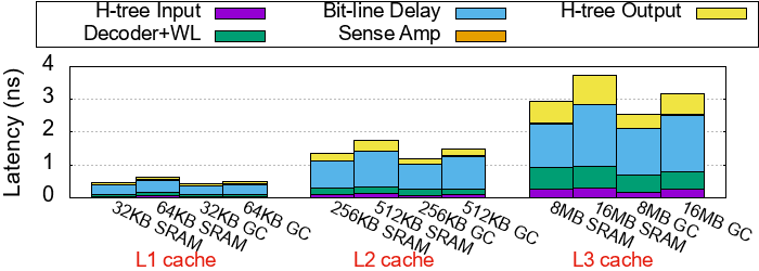
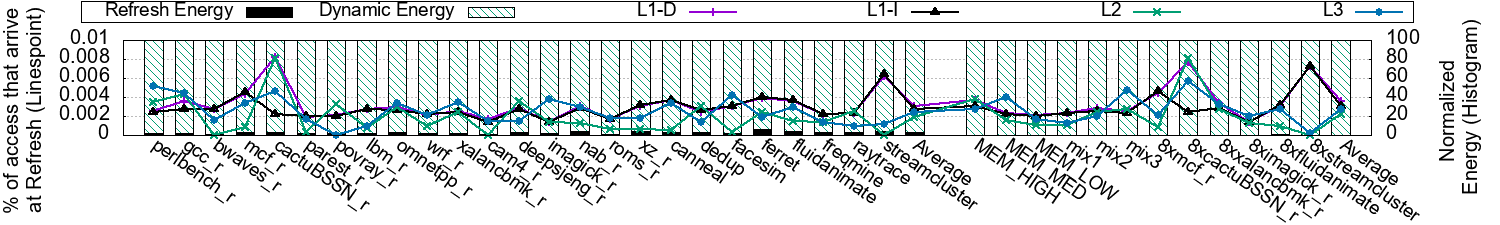
eDRAM has also been evaluated as a candidate for architecting caches (Chang et al., 2013; Wilkerson et al., 2010). It has found adoption in multiple recent products, including IBM’s Power series (Warnock et al., 2015), Intel’s Haswell (Hammarlund et al., 2014) and Microsoft’s Xbox 360 (Andrews and Baker, 2006), again as a technology for LLCs. Since eDRAM is a DRAM variant, it provides higher density compared to SRAM and has favorable access latency profiles (Chang et al., 2013) as compared to NVMs. However, the traditional 1T1C eDRAM cells suffer from low Data Retention Times (DRTs) of 20 - 50 s (Chang et al., 2013), requiring frequent refreshes in many eDRAM based design. These refreshes cause significant energy consumption as the data from an eDRAM row has to be read and written back (Chang et al., 2013; Wilkerson et al., 2010), making addressing refresh operations as the primary challenge in designing eDRAM caches. The energy consumption breakdown of dynamic and refresh energies for single programmed SPEC CPU2017 and PARSEC workloads in an eDRAM LLC (simulation parameters are listed in Section 7) is shown in Figure 1. As can be observed, refresh energy is many times higher than dynamic energy, which makes optimizing refresh operations an essential consideration for designing eDRAM based caches.
Apart from energy overheads, an eDRAM row, and hence a portion of the cache, is unavailable for the duration of the refresh period, leading to performance overheads. To counter the shortcomings of traditional eDRAM, another eDRAM variant, Gain Cell (GC) has been proposed (Somasekhar et al., 2009; Giterman et al., 2016), which has multiple advantages over 1T1C eDRAM. These include a cheaper, logic-compatible fabrication process and the absence of a dedicated capacitor per cell; GCs use the transistor’s parasitic capacitance for data storage. Finally, GCs provide non-destructive reads (Chang et al., 2013) and decoupled read/write bitlines, resulting in lower access latency and energy consumption (Somasekhar et al., 2009).
Despite these advantages, traditional 2T and 3T GCs have not found adoption widespread since they suffer from low DRTs, hence requiring frequent refreshes. While 4T GCs with higher DRTs have been proposed (Giterman et al., 2018), they suffer from higher write energies and lower density, making them unattractive as 1T1C eDRAM replacements. In any case, the presence of refresh makes existing GCs useless at any level of cache, other than LLCs (Chang et al., 2013).
As a result, even though each one of these technologies has its pros and cons, they cannot be used as a drop-in replacement for SRAM caches, especially for levels closer to the CPU. However, in the presence of a suitable SRAM replacement, many of their pros can be combined to architect high capacity caches that have similar latency profiles as that of an SRAM based hierarchy. In this paper, we attempt such a design, starting from ground up. First, we propose a novel FDSOI MOSFET (FDX, [n. d.]) based 2T Gain Cell, which provides high storage density, low access latencies, and a high DRT. This makes the cell amenable for use at all levels of the cache hierarchy. Even after accounting for peripheral circuitry overheads, compared to 6T SRAM, the proposed GC array offers a 50% reduction in read/write energies, 50% reduction in the area while keeping access latency unchanged. It exhibits low leakage energy and has modest refresh requirements. A comparison of advantages of the proposed GC over competing memory technologies for caches is presented in Table 1. The main contributions of this work are summarized below:
-
•
We propose a novel, FDSOI based 2T Gain Cell, specifically for use in on-chip caches, and exploit its back-gate bias feature to reduce leakage power by 99% and increase retention time by ~60, compared to conventional GC and eDRAM, reducing the need for frequent refreshes. We combine this already large refresh window with optimizations like staggered refresh, to design practically refresh-free GC caches. As a result, proposed GCs can be used at all levels of the cache hierarchy.
-
•
We show that GC based sub-arrays exhibit 2 area advantage and similar latency characteristics as compared to SRAM, even after accounting for overheads of peripheral circuits. This helps architect higher capacity caches within the same area and latency budgets. As a result, for single-programmed workloads, iso-area caches architected using proposed GCs at all levels of the hierarchy exhibit a 42% reduction in dynamic energy and a 29% increase in IPC as compared to SRAM. Multi-programmed workloads exhibit similar behavior. We further show that the proposed GC scales well at smaller technology nodes, and retains its advantages over SRAM.
-
•
We utilize the inherent decoupling in the read and write bitlines in proposed GCs to save precharge energy between consecutive writes, and clubbing up to 70% writes with reads, thereby improving performance and reducing dynamic energy consumption by 13%, as compared to GC based caches lacking this optimization. We also explore optimizations like no-refresh policy, where a line is invalidated if it is not accessed during its DRT period, and show that this can be used as an effective mechanism to eliminate refreshes in caches closer to the CPU without performance penalties.
-
•
Finally, to create high capacity, low latency caches, we evaluate several hybrid cache hierarchies by incorporating emerging technologies like STT-RAM with GCs to design caches that can provide up to 4 higher capacity, compared to iso-area SRAM caches. For multi-core workloads, hybrid caches architected with GCs, combined with asymmetric writes optimization, can provide 43% performance and 44% energy benefits as compared to iso-area SRAM caches.
The remainder of this paper is organized as follows. We provide the circuit level implementation details for proposed GC in Section 2 and details of the architectural implementations of GC caches in Section 3. Section 4 presents the experimental evaluation setup, while Section 5 analyses the energy and performance implications of the implementations. Section 6 proposes optimizations by exploiting intrinsic properties of GC, while Section 7 evaluates hybrid cache hierarchies. Sections 8 discusses the scalability of GC at lower technology nodes and provides an assessment of the no-refresh policy. Finally, we discuss related work in Section 9 and conclude in Section 10.
2. Back-Gate Biased Gain Cell
Gain Cells have started gaining traction owing to their logic-compatible fabrication process, small area footprint, and low energy requirements (Giterman et al., 2016, 2018; Teman et al., 2014; Somasekhar et al., 2009). GCs have been fabricated and tested in FinFET (Shalom et al., 2018), bulk (Ando, 2003), and FDSOI (Giterman et al., 2018) processes. However, these proposals still suffer from low DRT leading to enormous refresh energy, as shown in Table 1. Earlier, FDSOI devices have been fabricated in 12 nm (Glo, 2018) and are expected to scale down, considering their advantages of higher DRT over FinFET(Cheng et al., 2015; Johnson, 2018). We implement an n-type 2T GC on an FDSOI device (Planes et al., 2012; FDX, [n. d.]) and exploit its back-gate bias feature to lower the leakage current, thus improving the DRT.
2.1. Using Back-gate Biased FDSOI to increase DRT
Data retention time (DRT) of a transistor is directly linked with the leakage current of the transistor in the OFF condition. The leakage current (), in turn, exponentially depends on the threshold voltage () of the transistor. In the recent past, with technology scaling, leakage has prohibitively increased in bulk-MOSFETs necessitating significant manufacturing efforts and additional fabrication steps to control the leakage current. Silicon-on-Insulator (SOI) technology offers a promising solution to deal with leakage current due to an additional handle to control the threshold voltage using its back-gate biasing. The junction leakage currents are significantly reduced in a fully-depleted SOI (FDSOI) as an oxide layer removes the p-n junction from the substrate, and has been used in a few commercial offerings, including IBM’s POWER 8 (Fluhr et al., 2014). Due to this oxide layer, the substrate works as a second gate or the back-gate(Sellier, 2018), and can be biased to change the threshold voltage of the FDSOI transistor which, in-turn, exponentially reduce the leakage current (Ashenafi and Chowdhury, 2018; Clerc et al., 2015; Mohammed et al., 2018; Yang et al., 2013; Vatanjou et al., 2016; Zaini et al., 2017), and increases the DRT of the transistor.
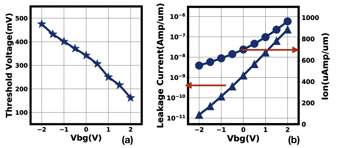
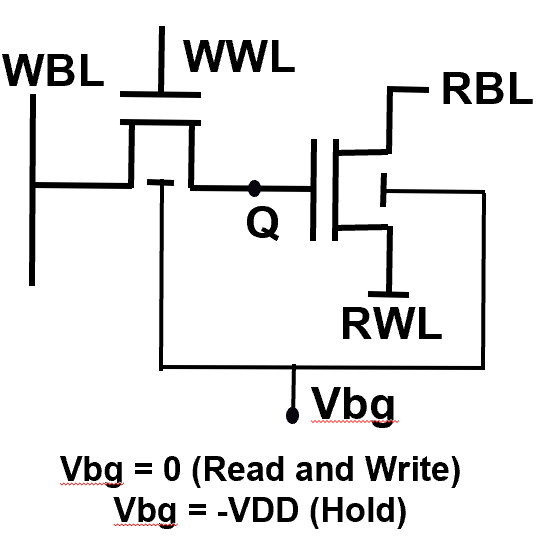
We have implemented the n-type transistor using ST Microelectronics 28-nm FDSOI technology and simulated it using Cadence Virtuoso. Figure 2(a) captures the effect of back-gate biasing () on threshold voltage, when is varied between to . Figure 2(b) shows the exponential dependence of on , and as becomes more negative, the leakage current exponentially drops by almost four orders of magnitude, up to 10 pA/m. Figure 2(b) also shows the improvement on (on-current) when is positive. Improvement in makes the transistor operate faster, thus reducing delay. Thus, back-gate biasing can be used both to improve performance (latency) and reduce leakage. The schematic of the proposed FDSOI based Gain Cell is shown in Figure 3a. During hold condition, -VDD is applied to the back-gate bias of the device, which reduces the leakage from W1, improving DRT.
2.2. Overheads of back-gate biasing
Leveraging back-gate bias for DRT improvement leads to the reduction of ON current of n-type FDSOI, as depicted in Figure 2(b), and hence, higher cell access latency. To capture the best of both worlds, we apply zero back-gate bias during read and write operations, and -VDD during the hold condition. This can be implemented with the circuit proposed in (Chhabra and Rana, 2016).
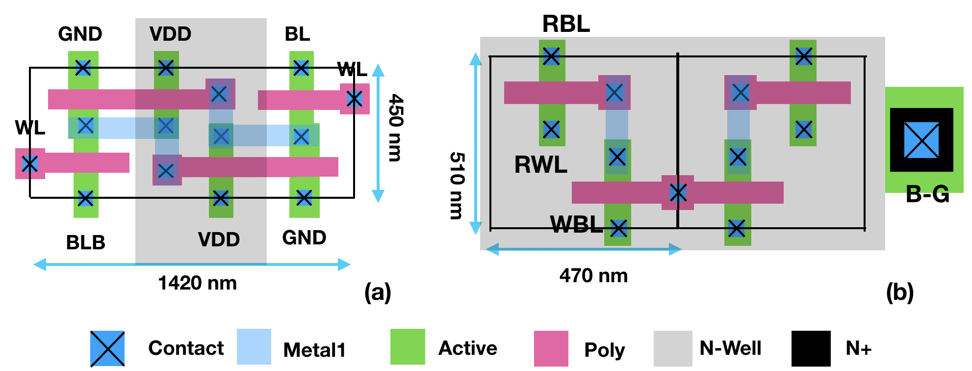
Figure 4 shows the layouts of SRAM and proposed 2T GC. To implement back-gate bias, a single contact can be shared across all the cells of a row in an array (as shown in Figure 4(b)). This keeps the area overhead minimal. Since the back-gate oxide thickness is quite large (~20 nm), back-gate carries only 5% of the front-gate capacitance, which keeps switching power overhead less than 5%, while increasing DRT. Additionally, since Vbg and row-signal (WWL) switching happens in parallel, delay of back-gate is over-shadowed by WWL’s delay. Hence, back-gate bias causes no latency penalty, negligible area penalty, and has only ~5% of the switching power overhead.
2.3. Working of Back-Gate Biased Gain Cell (BGB-GC)
Figure 3(a) shows the schematic of the proposed n-type 2T GC. GC has decoupled read and write operations and has non-destructive reads, unlike 1T1C eDRAM. The input signals for these operations are illustrated in Table 2. Working of proposed 2T GC is similar to conventional 2T GC, except that we use back-gate bias during hold condition.
2.3.1. Write Operation
Write Bitline (WBL) is shared across an entire column in an array and has a large capacitance. Write Wordline (WWL) runs along the row in the array. To write to the cell, data is first transferred to WBL, and then a row-signal (WWL) is used to transfer data to the Q node.
| Operation | WBL | WWL | Back-gate(bg) | RBL | RWL |
|---|---|---|---|---|---|
| Read | 0 | 0 | VDD(floating) | 0 | |
| Write | Data | VDD | 0 | VDD | VDD |
| Hold | 0 | -VDD | VDD | VDD |
2.3.2. Read Operation
For a read operation, Read Bitline (RBL), which is a shared signal across the column, is first precharged to VDD. Then, to read data, RBL is kept floating. Active low signal to Read Wordline (RWL) is used to read the data. If data stored in Q is 1, RBL discharges; otherwise it remains at VDD, which is sensed by a sense amplifier. During the read operation, energy is consumed in the switching of RBL and RWL. Most importantly, read operation in GC is non-destructive, since RBL is decoupled from the Q node (Somasekhar et al., 2009).
2.3.3. Hold Condition
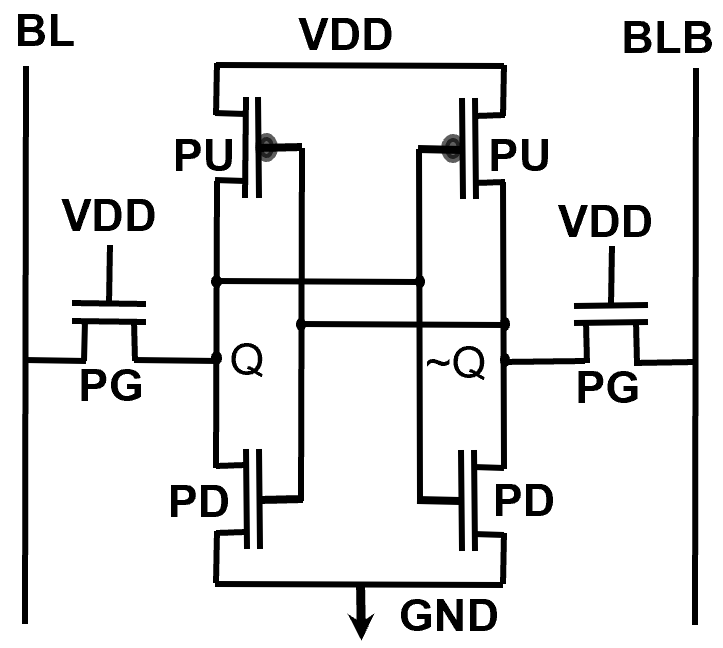
Periods where the cell is neither read nor written to is known as the hold condition. This is important since the cell still needs to retain data during this period, unlike SRAM where data is retained due to cross-coupled inverters shown in Figure 3b. The charge in Q node leaks from W1 over time, necessitating refresh operations for data restoration, before the DRT window closes.
2.4. BGB-GC comparison with 6T SRAM
2.4.1. Data Retention Time (DRT)
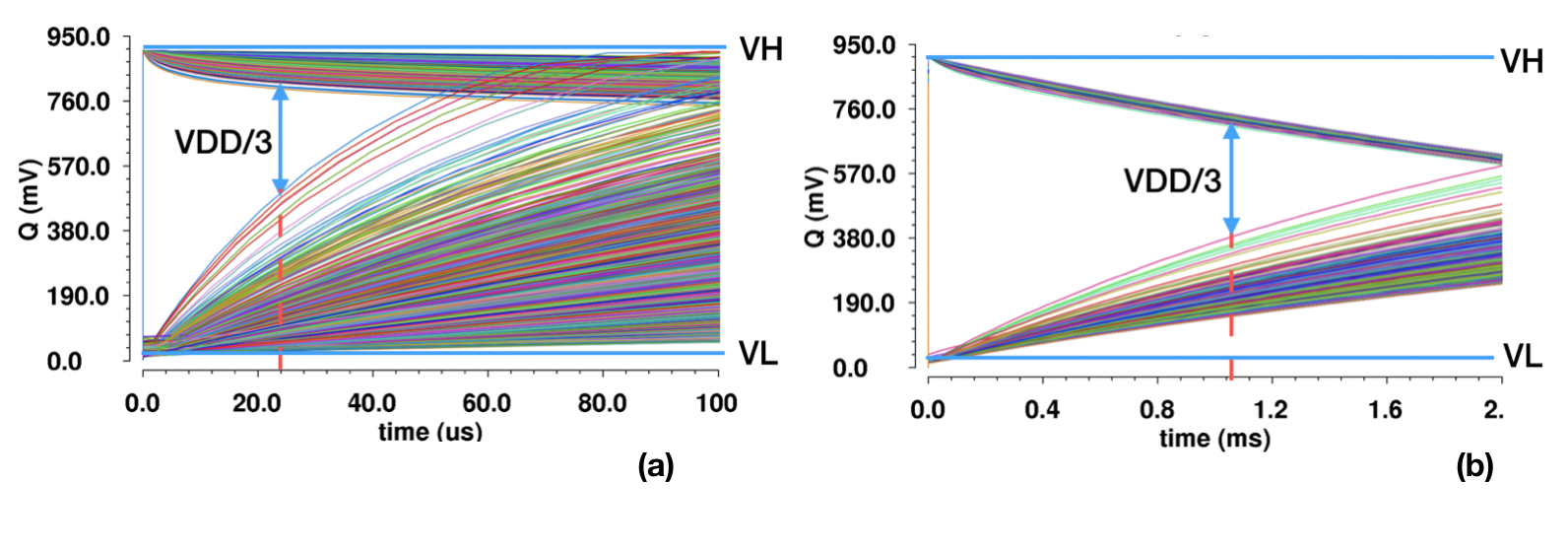
The proposed GC uses back-gate bias voltage of -VDD during hold operation, leading to reduction in leakage current from the W1 transistor, improving DRT. To quantify DRTs, we performed Monte Carlo simulations considering the standard 6- local and 1- global process variations. Figure 5 shows the data degradation of conventional and proposed 2T GC, for 10K M-C simulations. DRT is measured at a point where the data can be read without error. Typically, VDD/3 is a sufficient margin to read data properly, and we consider the worst-case DRT as the refresh interval, making these results more pessimistic than usual. For conventional 2T GC (Somasekhar et al., 2009), DRT obtained is 19s by considering 100% yield (Figure 5(a)), which is consistent with (Giterman et al., 2018). For the proposed GC, the data decay has significantly slowed down, as seen from Figure 5(b). We note that the worst-case DRT obtained for the proposed GC improves to 1.12 ms, which is ~60 higher than the case when no back-gate bias is applied. This is first such GC proposal built with 2 transistors leading to significant gains in DRT over existing GC designs, except 4T GC designs (Giterman et al., 2018) where a similar DRT is achieved at the cost of increased area and latency.
2.4.2. Leakage Power
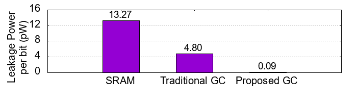
Since the proposed 2T GC has a smaller number of leakage paths compared to SRAM (schematic in Figure 3), it inherently has lower leakage power. Additionally, we have used back-gate bias to further reduce the leakage current significantly. We compare the leakage power of 6T SRAM, GC without back-gate bias, and proposed GC with back-gate bias in Figure 6. We show that proposed GC has ~99% reduction in leakage power as compared to 6T SRAM.
2.4.3. Area
Figure 4 compares the layout of the 6T SRAM cell and 2T GC at 28 nm technology. SRAM cell takes 0.64 m2, whereas the proposed GC takes 0.24 m2, which is 40% of the SRAM cell. The smaller size of the proposed GC allows for much higher density for the same area.
At the cell level, the proposed GC takes only 0.4 area compared to the 6T SRAM cell. Layout of the SRAM cell is drawn in a very efficient way and have area efficiency of 80%-90%(Karl et al., 2015; Weste and Harris, 2015; Rabaey et al., 2002). Considering this, at the cache level, GC can have ~2 capacity as compared to SRAM cache. Even though GC has 2.5 benefits at the cell level, at the cache level, it reduces to 2.0 due to peripheral circuitry overhead. In the rest of the paper, for the iso-area comparison, we have considered 2 capacity of GC compared to the SRAM.
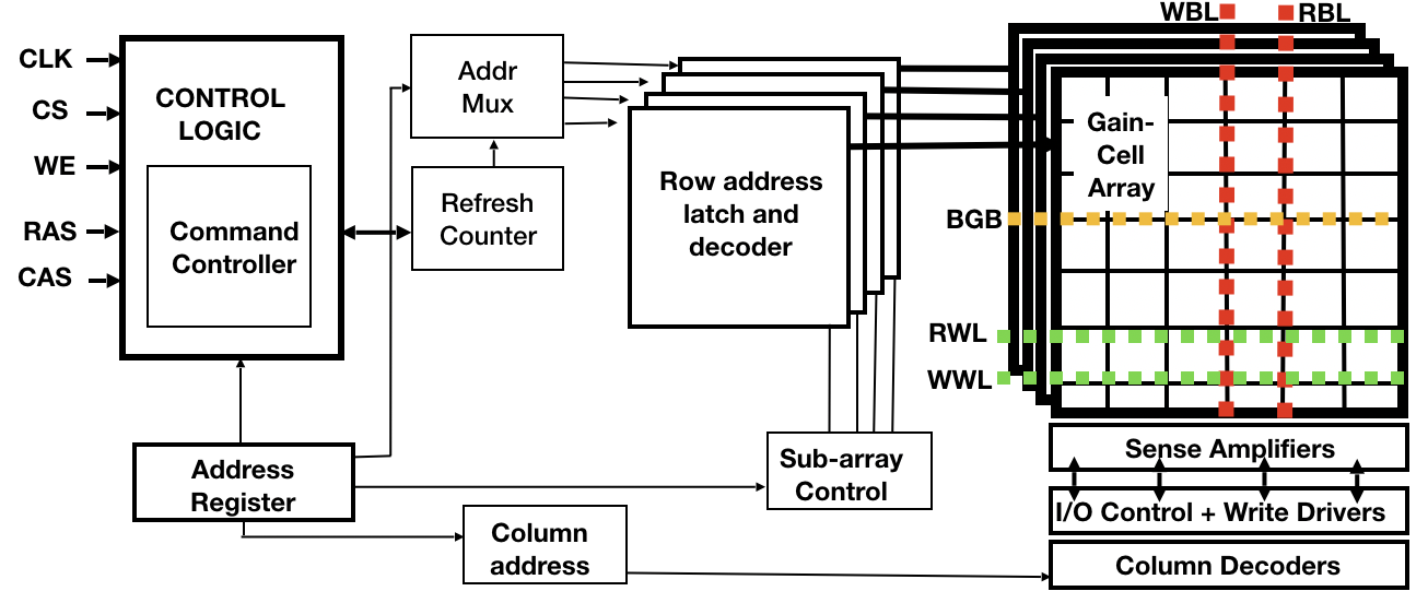
3. Architecting Gain Cells for Caches
First, we describe the sub-array construction of proposed GCs, and the mechanism by which it maps to various cache configurations. Then we compare the architectural benefits of GCs over SRAM.
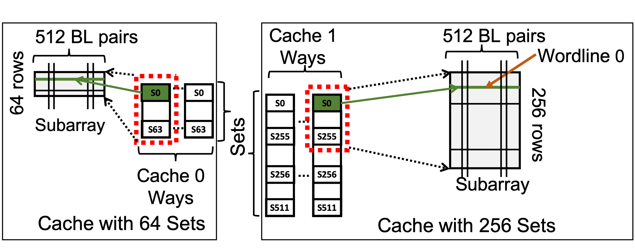
GCs are arranged as sub-arrays, in a typical row-column fashion. A cache can then be mapped to multiple sub-arrays, as dictated by its capacity. From an extensive design space exploration, we conclude that the sweet spot for minimum latency and peripheral circuitry overheads lie at a sub-array size of 256512 bits, or 16 KB. Hence, GC caches can be architected such that each way, across all cache sets, maps to one sub-array. As a result, looking up a cacheline (64B) is the same as looking up a row of this sub-array, as shown in the Set0-Way0 to Row0 mappings in Figure 7. In cases where combined size of a way is 16 KB, we keep adding sub-arrays, until all the sets have been accounted for. For example, the right hand side of Figure 7 depicts a cache where one way is mapped to two 256512 sub-arrays.
However, this prohibits mapping of any cache configuration where the combined capacity for one way is smaller than 16 KB, as illustrated in the left half of Figure 7. For these caches, we keep the design choice of mapping an entire way to one sub-array, while reducing the size of the sub-array. For example, in the case of a 64KB, 16-way cache, an entire way (4KB) is mapped to a 64512 bit sub-array. This ensures that a 64 B cacheline lookup is not spread across multiple sub-arrays.
| Cache Level | 32kB L1 | 256kB L2 | 8MB L3 | |
| Latency (ns) (in cycles) | SRAM | 0.475(2) | 1.34(5) | 2.81(10) |
| GC | 0.42(2) | 1.20(5) | 2.55(9) | |
| Read/Write Energy per bit (pJ) | SRAM | 0.75/1.13 | 2.18/3.1 | 7.5/11.8 |
| GC | 0.41/0.68 | 1.15/1.63 | 4.1/5.81 | |
| Write Energy/bit for Same Bit (0-0 or 1-1) (pJ) | SRAM | Same as Write Energy | ||
| GC | 0.24 | 0.7 | 1.95 | |
| Leakage/bit (pW) (SRAM/GC) | 13.27/0.09 | |||
| Refresh Interval(ms)/ Period per line(ns) | 1.12/1.5 | |||
| Refresh Energy/bit (pJ) | 1.87 | |||
Figure 8 shows the block diagram of the proposed GC cache. Compared to SRAM cache, GC has additional refresh counters at each level of cache. As per concurrent refresh, the refresh counter will generate signal to refresh the same row in all subarrays at the same time. BGB signal is generated along with RWL and WWL signals while performing refresh (no extra delay penalty). For staggering the refresh across different rows, the counter times out after every DRT/N time (N is number of rows in subarray).
Next, we compare and contrast the architecture level characteristics of on-chip caches devised using SRAM and GCs. We extract SRAM and GC energy and latency parameters using an enhanced CACTI (Muralimanohar et al., 2009) model and present these results in Table 3. These results were also validated using SPICE simulations using ST-microelectronics 28-nm FDSOI CMOS technology. We observe that for every cache level, the dynamic read and write energies for a GC cache are reduced by at least 50%, as compared to an SRAM one. This is because the proposed GC requires just one bitline per read or write access, thereby reducing a significant fraction of the dynamic energy consumed in switching of bitlines and word lines (Lee et al., 2013; Surana and Mekie, 2018).
Additionally, owing to decoupled read and write like 8-T SRAM(Rabaey et al., 2002) operations, GC has slightly lower access latencies as compared to SRAM, allowing for similar cycle time access as that of a SRAM cache, for a given processor frequency. Another trait of GC is high density, which enables us to fit a similar capacity cache in half the area. Alternatively, in a given area budget, we can implement a higher capacity cache by increasing associativity. As shown in Figure 9, iso-area access latencies of GC based caches at all levels of the hierarchy are similar to SRAM caches, with additional benefit of GC caches having twice the capacity. Doubling the capacity of an SRAM based cache increases the area by 2.0. Not only that, it also increases access latency of caches by at least 30%. As a result, GC based caches allow for twice the capacity in the same latency and area budget, for every level of cache.
3.1. GC Based Cache Proposals
Using these observations, we propose the use of GCs at various levels of caches, from all on-chip caches architected using GCs (ALL-GC) to just last-level cache (LLC-GC) or L1 cache (L1-GC) being GC, and compare with the baseline case where all caches are implemented with SRAM (ALL-SRAM). Since GCs provide excellent density benefits over SRAM, we examine the energy and performance implications of GC over SRAM for both iso (cache) capacity and iso-area. For iso-capacity (-CAP), SRAM and GC caches are compared with the same cache size, which indicates lower on-chip area usage by GC caches. While in the case of iso-area (-AREA), the GC caches are doubled in capacity by increasing their associativity, while retaining latency characteristics. We maintain the tag array in SRAM; only the data arrays are replaced with GCs.
3.2. Handling Refresh in Gain Cell Caches
One of the biggest challenges in GC caches is the need to refresh. In addition to adding energy overheads, the cache is made unavailable for access during refresh operations, which adversely affects performance. We use a staggered, concurrent refresh mechanism (Kirihata et al., 2005) to reduce unavailability of GC cache.
As explained earlier in this section, one way of the cache is mapped to a row in the GC sub-array. Refreshing one row of the sub-array takes 3 ns. We refresh one row in a sub-array at a time and iterate over all the rows in a round-robin fashion in the course of the 1.12 ms refresh window, which is the DRT of an individual cell.
A refresh is done by reading the sub-array in the first 1.5 ns of the refresh window. Data is written back to the row in the second half of the window. As a result, the sub-array is available for write in the first half and a read in the second half. This is made possible due to the presence of separate read and write bitlines. This optimization increases the availability of the sub-array and hence, the associated way – it is now unavailable only for 1.5 ns every 4.375 s. Since the tags are maintained in SRAM, the cache can still be accessed to check for hits/misses.
We carry out a detailed analysis of performance and energy implications of this refresh policy, in Section 5.3, and conclude that the performance overheads are minimal, since a tiny fraction (0.003%) of cache accesses happen concurrently with refresh, leading to a worst-case 1.7% reduction in performance, as compared to the SRAM baseline.
4. Evaluation Methodology
We evaluate our proposed architectures by using an 8-core system with configuration listed in Table 4, simulated using Sniper (Carlson et al., 2011). This configuration is used as the baseline for evaluation (ALL-SRAM). For iso-area GC caches (-AREA), cache capacity is doubled by doubling associativity. We test our proposals against 25 benchmarks from the SPEC CPU2017 (Singh and Awasthi, 2019) and PARSEC (Bienia et al., 2008) suites and study energy and performance implications in Sections 5.1 and 5.2, respectively. These workloads, listed in Table 5, are simulated for 2 billion instructions each, after a 500 million warmup period. Additionally, to include variations in the application behavior and test against multi-programmed workloads, we divide the workloads in six sets, each consisting of 8 benchmarks, which represents: memory-intensive applications (MEM_HIGH), applications with average memory access (MEM_MED), applications with sparse memory access (MEM_LOW), and three random mixes of 8-workloads (mix1-3). This classification is done based on memory accesses per kilo instructions to caches - higher accesses means more memory intensive. Also, we create six homogeneous multi-programmed workloads (8x*) - 8 copies of the same benchmark, each per core.
| Processor | 8-core, 3.4GHz, x86_64 ISA, 19-stage OOO | ||
|---|---|---|---|
| Decode, Rename, Fetch Width | 4-7 fused, 4, 6 instructions per cycle | ||
| Issue, Dispatch, Commit width | 4, 6, 4 fused -ops per cycle | ||
| ROB/Branch misprediction | 168 entries/8 cycles penalty | ||
| L1-I/L1-D cache | 32 KB, 8-way & 2 cycles. 64B line | ||
| L2 cache | 256 KB, 8-way & 5 cycles. 64B line | ||
| L3 cache | Shared 8 MB, 16-way & 10 cycles. 64B line | ||
| Main Memory |
|
| Single-Programmed |
|---|
| SPEC CPU2017 |
| perlbench_r, gcc_r |
| bwaves_r, mcf_r |
| cactuBSSN_r, parest_r |
| povray_r, lbm_r |
| omnetpp_r, wrf_r |
| xalancbmk_r, cam4_r |
| deepsjeng_r, imagick_r |
| nab_r, roms_r, xz_r |
| PARSEC |
| canneal, dedup |
| facesim, ferret |
| fluidanimate, freqmine |
| raytrace, streamcluster |
| Multi-Programmed | |||||||||
|---|---|---|---|---|---|---|---|---|---|
| MEM_HIGH | MEM_MED | ||||||||
|
|
||||||||
| MEM_LOW | mix1 | ||||||||
|
|
||||||||
| mix2 | mix3 | ||||||||
|
|
||||||||
| 8x* - Running 8 copies of the same benchmark | |||||||||
5. Evaluation of GC Caches
In this section, we quantify the benefits of various GC based architectures and compare them with SRAM based caches. The evaluation includes a study of memory subsystem energy, performance, and the impact of refresh operations.
5.1. Energy Analysis
While most emerging memory technologies exacerbate energy requirements of the memory subsystem (Zhang et al., 2014; Chang et al., 2013; Zhou et al., 2009a; Kültürsay et al., 2013), GCs, on the contrary, provide significant energy savings over SRAM. In comparison with the baseline SRAM, at the array level, proposed GC design consumes ~46% less energy per read and 40-50% less energy per write, as shown in Table 3.
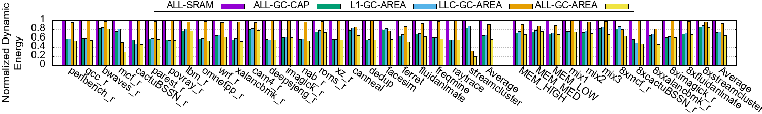
The ALL-SRAM case, where all levels of caches are assumed to be SRAM, is used as the baseline. We first study ALL-GC-CAP, where we replace all SRAM caches with the same capacity GC caches (iso-capacity). Next, we evaluate iso-area GC caches with double capacity. For this, we evaluate three configurations: (a) L1-GC-AREA, where we replace L1 cache in ALL-SRAM with a double capacity GC cache. (b) LLC-GC-AREA, where we replace last-level cache in ALL-SRAM with double capacity GC, and (c) ALL-GC-AREA, where we replace all levels of caches in ALL-SRAM with double capacity, iso-area GCs.
Figure 10 compares the dynamic energy consumed by the memory subsystem in proposed architectures, for both single and multi-programmed workloads. We calculate the dynamic energy consumption of caches and main memory by taking the product of the total number of accesses to each level with the energy consumption of per access using the per bit cache access energy (mentioned in Table 3). Access energies of main memory are obtained from (MIC, [n. d.]) and are presented in Table 4. We observe that any cache hierarchy devised using GCs exhibits savings in dynamic energy. In L1-GC-AREA, where only the L1 is architected using proposed GCs, results in a 36% reduction in dynamic energy, averaged across all the single programmed benchmarks. The LLC-GC-AREA configuration, which replaces the SRAM LLC with a double capacity GC cache, also exhibits a 4% average reduction in dynamic energy. Similar results are obtained for multi-programmed workloads as well. For the memory-intensive mix (MEM-HIGH), the energy savings of L1-GC-AREA and LLC-GC-AREA stand at 25% and 9%, respectively.
Finally, using GC for all levels of the cache increases these gains tremendously. On average, across the single programmed workloads, ALL-GC-AREA achieves 42% (34% in the case of multi-programmed) reduction in dynamic energy consumption as compared to the ALL-SRAM baseline. Even in cases where the area density benefits of proposed GC are not being utilized, i.e., in the sub-optimal configurations of ALL-GC-CAP, where all SRAM caches are replaced with equal capacity GC caches, we observe an average reduction in the dynamic energy of 34% and 28% for single and multi-programmed workloads respectively.
Compared to the baseline, applications like streamcluster and mcf_r, that have large number of memory accesses, achieve up to 80% reduction in dynamic energy for iso-area GC LLCs (LLC-GC-AREA). Increasing LLC capacity allows the working set of these applications to reside in the cache, reducing the number of off-chip accesses substantially (by ~99%). Reduced off-chip accesses reduce the high off-chip dynamic energy, resulting in massive energy savings. Additionally, in a large, many-core CPU running at a low voltage, leakage from on-chip caches contributes substantially to the chip’s power draw (Agrawal et al., 2013). Proposed GC, with a large savings of 99.3% in leakage energy, as depicted in Figure 6, helps reduce these costs substantially.
5.2. System Performance
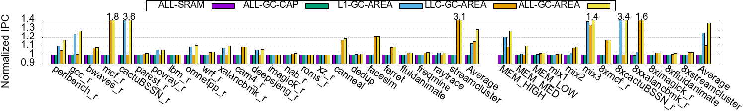
Figure 11 illustrates the system performance in terms of instructions per cycle (IPC) for various proposals, using single and multi-programmed workloads. We observe that the performance difference between iso-capacity SRAM caches (ALL-SRAM) and GC caches (ALL-GC-CAP) is negligible - 0.1% drop in IPC for GC caches on average, with respect to ALL-SRAM. All GC based iso-area caches (ALL-GC-AREA) exhibit performance gains as compared to the baseline. Average performance increase of 29% and 36% is observed across single and multi-programmed workloads, respectively. In the case of multi-programmed workloads, memory-intensive workloads tend to benefit most. We observe a 27% performance increase for MEM_HIGH workloads mix, as compared to the baseline. We verified our results on an aggressive processor configuration, with better prefetcher, replacement policy and DRAM access latency (Nesbit and Smith, 2004; Smith, 1982; Jaleel et al., 2010), and observed similar benefits (4% IPC drop from above reported benefits).
Applications like streamcluster, canneal, and mcf_r have working set sizes that exceed the capacity of baseline SRAM caches. Hence, when the LLC size is doubled (LLC-GC-AREA), they see large performance improvements (200%) as working sets can reside on caches. While, many applications like cactuBSSN_r and gcc_r have working sets that reside in the on-chip memory and leverage larger cache size to fit working sets in the L1 cache. As a result, they achieve significant performance improvements in L1-GC-AREA implementation (drop-in accesses to next level caches by 90%) but not in LLC-GC-AREA. On average, L1-GC-AREA and LLC-GC-AREA achieve IPC improvements of 13% and 15%, respectively.
5.3. Impact of Refresh
Regular GC based caches are required to refresh cells at regular intervals. Unfortunately, this has adverse effects on both energy and performance. 1T1C eDRAM and traditional 2T, and 3T GCs can have huge refresh energy overheads, accounting for up to 97% of total LLC energy, as was observed in the experimental results presented in Figure 1.
However, for caches designed using the proposed GC, owing to high DRTs and staggered refresh mechanisms, we observe that the refresh energy consumption is minimal, assuming the most pessimistic scenarios. For experiments carried out with an all GC based cache subsystem (ALL-GC-AREA), which should exhibit the worst case refresh energy consumption profile, we observe that on average, across all single programmed benchmarks, refresh energy contributes 3% (6%, at max for ferret) of the total energy consumption of all caches. We illustrate these observations in Figure 12. For this worst case, we show that refresh energy has an insignificant contribution to the total energy, as depicted in the histogram on y2-axis.
Besides, the refresh operations do not affect performance adversely, as demonstrated from ALL-GC-CAP results from Section 5.2. This is evidenced by the fact that caches spend only 0.008% of the time on refresh, on average. Our experiments show that, on average, ~0.003% of accesses to caches were made during refresh interval throughout the entire simulation (Figure 12, y1-axis).
6. Asymmetric Writes
To read/write a value in a 6T SRAM cell, the bitlines first have to be precharged to VDD. Then, wordlines are turned on to access the cell value. On a read, both bitlines are precharged to high (VDD) while on a write, one bitline is driven to high and other to low (Weste and Harris, 2015; Rabaey et al., 2002). In proposed GC, we have separate bitlines for read (RBL) and write (WBL), as depicted in Figure 3a. Due to this decoupling, there is no need to precharge the WBL to VDD before every access, unlike in SRAM where the bit lines are pre-charged to before every write. To perform a write, the WBL is precharged to high or low, depending on the value to be written. For instance, to write a , WBL will initially be connected to ground to establish the voltage difference to drain the charge in the cell to . Thus, if WBL was already set to , driving it again to would require no energy. Such cases arise when the consecutive writes by WBL are the same, i.e., or transitions. In these cases, the second write will have a lower energy consumption as compared to a similar transition in 6T SRAM, as depicted in Table 3.
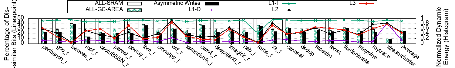
We quantify the overall dynamic energy savings due to such asymmetric writes by calculating the number of dissimilar bits between two consecutive writes. Dissimilar bit writes are serviced normally, while writes with similar bits are serviced with reduced energy. The reduced energy parameters for caches, extracted from CACTI, are depicted in Table 3. We perform this experiment with ALL-GC-AREA configuration and present our results in Figure 13. On y1-axis, we present the ratio of dissimilar bit writes to total bit writes, for each cache. Lower ratio implies that a lot of the data being written is similar to the value of the WBL, and hence can be written with lower write energy. Accordingly, we calculate the overall dynamic energy consumption (cache + main memory) and compare it with baseline ALL-SRAM and ALL-GC-AREA proposals on y2-axis. We observe that most bits – 76%, averaged across all levels of caches, in write data are similar to the write bitline’s value. SPEC CPU2017 workloads rarely have writes which are larger than 8Bytes (Singh and Awasthi, 2019). The rest of the cacheline is re-written with the same value. This is true for all data caches, with L1D exhibiting as high as 94% similarity, averaged across all benchmarks. Even in cases, where the initial access was a miss, and the existing cacheline has to be replaced with a new one being brought in, we observe significant data similarity between the new and the old lines. For instance, L1 I-cache, which only experiences writes as insertions of new cachelines, observes a 55% data similarity between the old and new lines. As a result, we observe a 13% reduction in dynamic energy consumption, with respect to ALL-GC-AREA, and 50% compared to baseline SRAM-based cache subsystem (ALL-SRAM). Applications with higher write ratios (Singh and Awasthi, 2019) tend to save more energy, for example, parest_r, omnetpp_r, xalancbmk_r, and povray_r. Therefore, we show that, because of its inherent structure, GC can take advantage of write similarity in data to further save on dynamic energy.
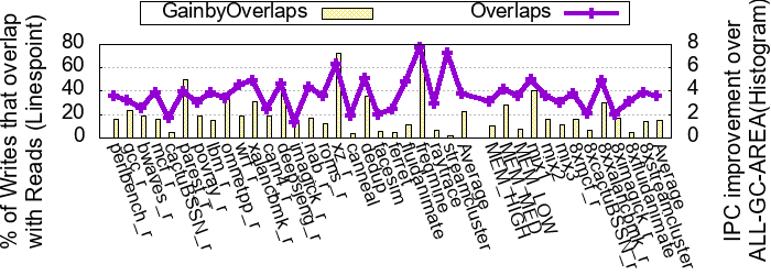
Additionally, due to decoupled bitlines, reads and writes to the same sub-array can be done in parallel. We use this property to overlap writes with simultaneously occurring reads to the same sub-array. We note that 40% of all writes could be overlapped with some reads, represented by line-graph Overlaps in Figure 14. Most of the overlaps happen in L1-D cache, as L2 and L3 caches have more sub-arrays and experience a smaller number of writes than L1. By hiding the latency of these writes, we observe a ~2% increase in IPC compared to ALL-GC-AREA, presented by GainbyOverlaps in Figure 14. To further take advantage of decoupled bitlines, smart cacheline placement policies or buffering can be used, which can potentially increase the number of overlaps. However, we do not pursue these optimizations due to the lack of substantial returns on either performance or energy.
7. Hybrid Cache Hierarchy
| eDRAM | STTRAM | Hybrid (8MB GC | |
| 32MB | 32MB | +16MB STTRAM) | |
| Read Latency (ns) (cycles) | 5.15 (18) | 26 (89) | 2.93 (10), 26 (89) |
| Write Latency (ns) (cycles) | 5.15 (18) | 60 (204) | 2.93 (10), 60 (204) |
| Read/Write Energy / bit (pJ) | 5.2/6.12 | 5.35/7.85 | 3.81/5.52, 5.35/7.85 |
| Refresh Interval/Period | 0.02ms/4ns | -/- | 1.12ms/1.5ns, -/- |
| Refresh Energy/bit (pJ) | 3.5 | - | 1.87/ - |
A growing body of research has proposed either eDRAM or STT-RAM as a replacement for LLCs ((Ahn et al., 2014; Chen et al., 2016; Khoshavi et al., 2016; Rasquinha et al., 2010; Smullen et al., 2011; Sun et al., 2009; Xu et al., 2011; Kang and Park, 2017; Lee et al., 2018; Agrawal et al., 2013, 2014; Chang et al., 2013)). In this section, we build on prior work to evaluate hybrid cache hierarchies, in an effort to build efficient SRAM “free” on-chip caches.
First, we compare proposed GC based caches with other, state-of-the-art memory technologies. We consider the architectures, where L1 and L2 caches are kept as GC and use either eDRAM or STT-RAM in LLC, namely “GC-GC-eDRAM” and “GC-GC-STTRAM” respectively. STT-RAM parameters were taken from (Lee et al., 2018), while parameters for eDRAM are obtained from CACTI simulations, and are listed in Table 6. In our experiments, we consider state-of-the-art refresh-optimized eDRAM (Agrawal et al., 2014) which achieves ~20 reductions in the number of refreshes over regular eDRAM at 2-3% area overhead.
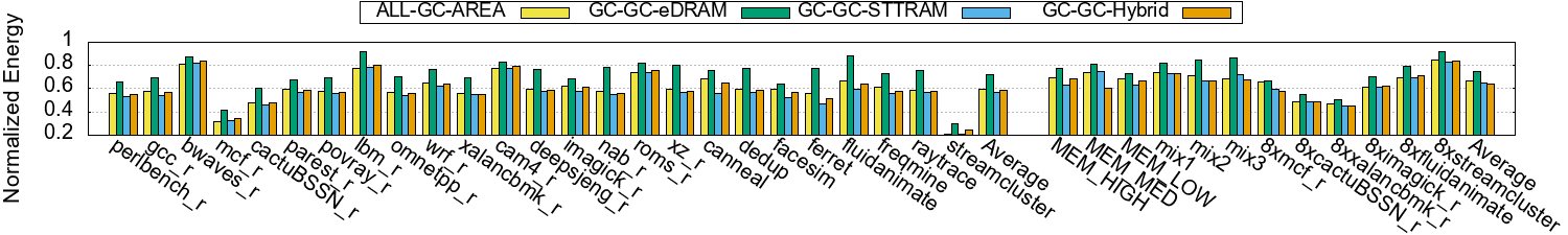
We compare these technologies with ALL-GC-AREA and present energy and performance comparisons in Figures 15 and 16, respectively. These experiments provide several interesting results. (a) eDRAM based LLC has 2 density benefits over GC, which helps it achieve 2.3% (4% for multi-core) improvement in IPC over ALL-GC-AREA, which makes a case for an eDRAM-based LLC. However, eDRAM has large refresh overheads. Even the refresh-optimized eDRAM (Agrawal et al., 2014) (GC-GC-eDRAM) results in 21% (12% for multi-core) more total energy consumption than ALL-GC-AREA. Traditional eDRAM results in much worse energy overheads – 6.8 higher energy consumption as compared to ALL-GC-AREA.
STT-RAM, with the same 2 density benefits over GC, suffers from much longer access latencies, which have been enumerated in Table 1. As a result, configurations with STT-RAM LLC experienced a performance drop of 7% with respect to ALL-GC-AREA, even though the number of off-chip requests actually dropped significantly by 13%. However, in realistic cases (multi-core runs) that take advantage of larger LLC, GC-GC-STTRAM performs slightly better than ALL-GC-AREA. Consequently, with smaller off-chip accesses, energy consumption reduces by 5%, compared to ALL-GC-AREA, concluding that STT-RAM LLC would be a better design.
In an effort to get the best of all worlds: utilize higher density of STT-RAM, and low latency of GC, we propose hybrid LLC designs of GC and STT-RAM. We selected STT-RAM to avoid the high energy overheads imposed by eDRAM. We carried out a design space exploration for the optimal size partitioning between GC and STT-RAM, while maintaining the same area budget as SRAM, and found that equal-area (8 MB GC, 16 MB STT-RAM) distribution results in the sweet spot of high performance and low energy. The parameters of this organization are listed in Table 6. The ways of each set of the hybrid cache are split between GC and STT-RAM cachelines, in the ratio of capacity. On a cache lookup, tags of both GC and STT-RAM ways are read and compared. If there is a hit in one of the GC ways, a read or write is carried out. On a miss in GC ways, but a hit an STT-RAM way, the cacheline is moved to the LRU position in the GC ways. Since GC ways tend to have “hot” data, in order to exploit temporal locality, the evicted cacheline from GC way is moved to the LRU position of the STT-RAM ways. In case of a miss in both GC and STT-RAM ways, the cacheline is fetched from the next level and placed in the LRU position of STT-RAM ways. The proposed hybrid cache architecture can be further optimized via novel replacement policies and prefetchers, which we leave for future work (Ahn et al., 2015; Kim et al., 2018). With L1 and L2 cache as GC, and a hybrid LLC, we evaluate the architecture, results of which are compiled in orange bars of Figures 15 & 16, under “GC-GC-Hybrid”.
As expected, the energy consumption of hybrid design is very close to that of ALL-GC-AREA: within 2%, on average, across both single and multi-core benchmarks. More importantly, the increased LLC accesses, due to larger cache, are performed with lower latencies of GC. As a result, we observe 5% improvement in IPC over ALL-GC-AREA baseline, averaged across multi-core simulations. Compared to the traditional SRAM hierarchy, our proposal shows 24% better performance with 42% less energy consumption (43% better with 36% less energy, in case of multi-core). These designs can be further optimized by exploiting decoupled bitline optimizations proposed previously, resulting in an extra 13% savings in energy, as discussed in Section 6, leading to overall 50% (44% in case of multi-core) saving in energy as compared to ALL-SRAM. In conclusion, while GC works best for L1 and L2 caches, real environments require large-capacity LLC with low latency, which can be addressed with our proposed GC-STTRAM hybrid LLC design. In the hybrid design, we move the recently accessed cachelines to the GC part of hybrid LLC, thus serving them with lower latency, if locality exists.
In summary, we present Energy-Delay Product (EDP) results of various architectures in Figure 17. As can be observed, for both single and multi-programmed workloads, any GC based hierarchy does better than the baseline SRAM one. The most favorable design point is obtained by utilizing the benefits of asymmetric write - optimized GC caches at all levels, and a hydrid STT-RAM - GC LLC. This architecture achieves an EDP which is 0.46 of the baseline SRAM one.
8. Scalability of Proposed Caches
As the technology scales down, transistors become leakier with smaller storage capacitances, resulting in smaller DRTs, exacerbating the refresh problem. This means that at lower technology nodes, GC based caches, due to a large number of refreshes, could perform worse than traditional SRAM based caches. To understand scalability characteristics of proposed GCs, we carry out experiments to characterize the energy consumption of proposed GC with technology scaling.
We carry out our analysis for 28, 22, 14, 10, and 7 nm technology nodes. Generally, leakage current and device capacitance are inversely proportional to technology node (ITR, [n. d.]; Weste and Harris, 2015). So, scaling down to the next technology node would result in DRT reduction by ~%. Additionally, cell access energies also decrease by ~% as we move to lower technology (Weste and Harris, 2015). Considering these trends, we simulate ALL-SRAM and ALL-GC-AREA configurations and calculate dynamic and refresh energy consumptions. At each technology node, we normalize ALL-GC-AREA’s energy consumption (dynamic + refresh) compared to ALL-SRAM’s energy consumption (dynamic) and present the results in Figure 18. Due to space constraints, we present only 15 benchmarks, 5 each from different memory intensity groups listed in Table 5. The first five benchmarks are from MEM_HIGH, followed by MEM_MED and MEM_LOW.
We observe that as we move to lower technology nodes, the contribution of refresh energy increases considerably. At 7 nm, the energy consumption of GC based caches (ALL-GC-AREA) is almost comparable to SRAM based caches (ALL-SRAM). Therefore, at 7 nm or lower, proposed GC, due to refresh, can perform worse than SRAM. Many techniques (Agrawal et al., 2013; Wilkerson et al., 2010; Agrawal et al., 2014; Tu et al., 2018) have been explored to reduce refreshes if it becomes a problem. We propose to reduce the refresh energy by increasing the back-gate bias voltage. Figure 2 shows reduction in leakage current with increasing back-gate bias voltage in a negative direction. This increases the cell’s DRT, which decreases refresh frequency and hence, energy. In Figure 19, for three technology nodes, we show that the actual DRT of rows can be much higher than the worst case, for which we have to design refresh mechanisms. A potential solution to avoid that could be to use architectural solutions like RAIDR (Liu et al., 2012) and implement separate refresh intervals for different rows based on their actual DRTs. This can be achieved by dividing the rows into DRT bins and applying a different refresh interval for each bin, leading to a reduction in the number of refresh operations.
8.1. Refresh Free Hybrid Cache Hierarchy
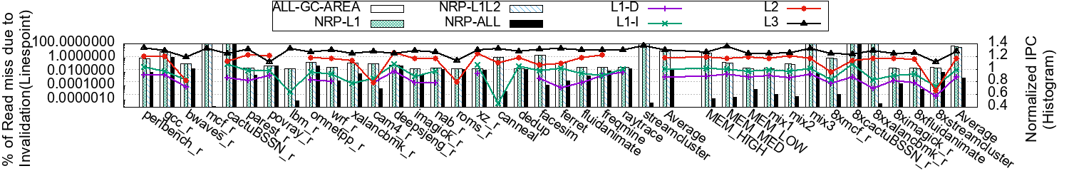
Another key solution which reduces the effect of refresh is a No Refresh Policy (NRP), where rather than refreshing a cacheline, we invalidate the data if the line has not been touched after a refresh operation has been performed, but before it reaches its DRT. The key observation here is that if a row is accessed, the countdown for its DRT is reset, starting the refresh window from that point. NRP can further be optimized by taking advantage of the high number of writes in caches to reduce such invalidations (similar to (Ghosh and Lee, 2007)). To invalidate GC cachelines, a dedicated, on-chip refresh controller, which generates a pulse at given intervals would be required (Agrawal et al., 2013; Gulur et al., 2016). We propose to maintain a 5-bit (programmable) saturating counter for every cacheline, which is incremented every epoch of the refresh interval. Once the counter saturates, the cacheline is invalidated. If the cacheline was dirty, it is written back to the next level of the hierarchy. In case of a write to the cacheline, the counter is reset to 0. We implement this policy at 28nm and calculate the number of times a cacheline was invalidated due to DRT expiration and present the percentage of cache read misses due to such invalidations on the y1-axis of Figure 20 and the performance impact of these invalidations on the y2-axis. We observe that NRP in L1 and L2 caches does not cause many misses (1%), and exhibits similar performance as compared to GC with refreshes - on average, 0.1% and ~1% drop in IPC, for single and multi-programmed workloads respectively. However, extending NRP to LLC generates ~12% new misses due to invalidations. It, therefore, results in 23% (36% for multi-programmed workloads) drop in IPC (as seen from Figure 20) as a miss in LLC results in a request to the main memory. Also, while invalidating, we writeback dirty cachelines. This has negligible (10MB/s) bandwidth impact on L1 and L2 bandwidth, but results in an average memory bandwidth usage of ~110MB/s across multi-core workloads, which is small but may be unacceptable in many cases. Although NRP doesn’t generate many new writebacks because it preemptively invalidates cachelines which would otherwise have been dirty evictions. NRP can altogether remove refreshes, and hence refresh energy, from L1 and L2 caches, while L3 cache would still need to be periodically refreshed. However, implementing L3 with STT-RAM does not need not refresh. As a result, we conclude that a hybrid cache hierarchy, where the L1 & L2 comprise of proposed GC, and LLC is made from STTRAM-GC hybrid is the lowest energy, highest performance on-chip cache hierarchy with refresh-free L1 and L2 caches.
9. Related Work
Emerging Memory Technologies for Caches: Due to scalability and energy issues of traditional SRAM, several studies have been carried out to evaluate emerging memory technologies for caches. STT-RAM, owing to its low leakage energy and density benefits, has been viewed as a promising candidate. However, it suffers from inherent weaknesses - high write latency and write energy. There have been many proposals to alleviate these shortcomings (Jog et al., 2012; Imani et al., 2016; Khoshavi et al., 2016; Samavatian et al., 2014; Wang et al., 2014; Zhou et al., 2009b; Smullen et al., 2011; Rasquinha et al., 2010; Chen et al., 2016; Sun et al., 2009; Ahn et al., 2014).
Another potential replacement for SRAM are eDRAMs, which offer high density, low leakage, similar access latencies, and low dynamic energies. However, eDRAM requires refresh operations to preserve data integrity (Jing et al., 2013). As cache size increases, each refresh requires more energy, and more lines need to be refreshed; thus, refresh can potentially become the main source of eDRAM power dissipation. Many studies have been carried out to amortize this effect (Wilkerson et al., 2010; Tu et al., 2018; Agrawal et al., 2013; Chang et al., 2013; Wu et al., 2009; Mangalagiri et al., 2008; Gulur et al., 2016). For instance, (Agrawal et al., 2014) showed that the DRTs of cells in large eDRAM modules exhibit spatial correlations, and exploit this behavior to reduce refresh energy. In contrast, the proposed GC already has insignificant refresh overheads.
Gain Cell: Many circuit and array level architectures have been proposed for GCs (Ando, 2003; Chun et al., 2011, 2012; Krautschneider and Klingenstein, 1994; Somasekhar et al., 2009; Giterman et al., 2016, 2018, 2018; Choi et al., 2015; Kazimirsky et al., 2017). The biggest advantage of the GC is its logic compatible fabrication process - only transistors are used for designing the cell and, therefore, can use the same fabrication process as the processor. Transistor’s parasitic capacitor is used to store the data. Due to low storing capacitance and high leakage of the junctions in bulk-MOSFET (Weste and Harris, 2015), DRT of GC is tiny. To improve DRT, Robert et al.(Giterman et al., 2018) propose using FDSOI-MOSFET instead of bulk-MOSFET or FinFET, which has reduced leakage current as the junctions are isolated in FDSOI through the oxide (Planes et al., 2012). The other added advantage of the FDSOI device is its back-gate bias feature (Ashenafi and Chowdhury, 2018). While body-bias can also be applied in bulk devices to improve the DRT (Meinerzhagen et al., 2013), it has limited breakdown voltage and can only be applied in p-type MOSFETs (Weste and Harris, 2015). In contrast, a large back-gate bias can be applied in FDSOI technology.
In the FDSOI device, threshold voltage and leakage of the device can be changed dynamically with the help of the back-gate bias. Many designs (Mohammed et al., 2018; Yang et al., 2013; Vatanjou et al., 2016; Zaini et al., 2017) have been proposed by exploiting the back-gate bias feature of the FDSOI. (Ashenafi and Chowdhury, 2018) designed the power gating circuit with the help of the back-gate bias feature of the FDSOI device. Clerc et al. (Clerc et al., 2015) designed the robust multiplier and DC-to-DC converter by exploiting the back-gate bias feature. In (Giterman et al., 2018), GC is implemented using FDSOI-MOSFET for its low leakage feature and uses 2 additional transistors to improve DRT at the cost of the area.
Architectural optimizations for SRAM caches: Many schemes have been looked into to reduce SRAM’s leakage energy (Kaxiras et al., 2001; Flautner et al., 2002). To catch up with the increasing demands for large capacity caches, numerous cache compression techniques have been looked into (Mittal and Vetter, 2016; Panda and Seznec, 2016; Arelakis et al., 2015). Also, there has been a significant amount of work on achieving higher performance in caches. Studies have been carried out for efficient cache replacement and cache management policies (Chaudhuri, 2009; Jaleel et al., 2010; Qureshi et al., 2007; Qureshi et al., 2006; Manikantan et al., 2012), dead block predictions (Lai et al., 2001; Khan et al., 2010; Manikantan et al., 2011), or exploiting the differences between reads and writes in caches (Khan et al., 2014; Wang et al., 2012).
10. Conclusion
In this work, we propose a novel FDSOI based 2T Gain Cell (GC) as a promising candidate for use in all levels of on-chip caches. The proposed GC has better energy efficiency, a much smaller area footprint, and better scalability as compared to 6T SRAM. Using the back-gate bias feature of FDSOI, we improve GC’s data retention time, minimizing contribution of refresh to the overall energy consumption of the cache hierarchy.
We evaluate various architectural implementations of GC, for all levels of on-chip caches and demonstrate that GC based caches substantially reduce the dynamic energy consumption of memory subsystem as compared to traditional SRAM caches. We exploit the inherent capabilities of the proposed GC, including decoupled read and write bitlines, to further reduce dynamic energy. Next, we demonstrate that a no-refresh policy, where GC based cache lines are invalidated than refreshed, can be a viable implementation for removing refreshes in GC caches closer to the CPU. Finally, we show that proposed GC, in conjunction with emerging memory technologies like STT-RAM can be used to architect SRAM-free cache hierarchies with a much superior energy-delay product as compared to SRAM caches.
References
- (1)
- FDX ([n. d.]) [n. d.]. FDSOI 28 nm Technology. http://www.st.com/b/content/st_com/en/about/innovation---technology/FD-SOI.html.
- ITR ([n. d.]) [n. d.]. ITRS Scaling. http://www-inst.eecs.berkeley.edu/~ee130/sp06/chp7.pdf.
- MIC ([n. d.]) [n. d.]. Micron Technical Note TN-41-01. http://www.micron.com/products/support/power-calc/.
- Glo (2018) 2018. 12FDX. https://www.globalfoundries.com/technology-solutions/cmos/fdx/12fdx/.
- Adkisson et al. (2002) James W Adkisson, Ramachandra Divakaruni, Jeffrey P Gambino, and Jack A Mandelman. 2002. Embedded DRAM on silicon-on-insulator substrate. US Patent 6,350,653.
- Agrawal et al. (2014) Aditya Agrawal, Amin Ansari, and Josep Torrellas. 2014. Mosaic: Exploiting the spatial locality of process variation to reduce refresh energy in on-chip eDRAM modules. In Proceedings of the 20th International Symposium on High Performance Computer Architecture (HPCA).
- Agrawal et al. (2013) Aditya Agrawal, Prabhat Jain, Amin Ansari, and Josep Torrellas. 2013. Refrint: Intelligent Refresh to Minimize Power in On-chip Multiprocessor Cache Hierarchies. In Proceedings of 19th International Symposium on High Performance Computer Architecture (HPCA).
- Ahn et al. (2014) Junwhan Ahn, Sungjoo Yoo, and Kiyoung Choi. 2014. DASCA: Dead write prediction assisted STT-RAM cache architecture. In Proceedings of 20th International Symposium on High Performance Computer Architecture (HPCA).
- Ahn et al. (2015) Junwhan Ahn, Sungjoo Yoo, and Kiyoung Choi. 2015. Prediction hybrid cache: An energy-efficient STT-RAM cache architecture. IEEE Trans. Comput. (2015).
- Ando (2003) Yoshiyuki Ando. 2003. Capacitorless DRAM gain cell. US Patent 6,560,142.
- Andrews and Baker (2006) Jeff Andrews and Nick Baker. 2006. Xbox 360 system architecture. IEEE micro 26, 2 (2006), 25–37.
- Arelakis et al. (2015) Angelos Arelakis, Fredrik Dahlgren, and Per Stenstrom. 2015. Hycomp: A Hybrid Cache Compression Method for Selection of Data-type-specific Compression Methods. In Proceedings of the 48th International Symposium on Microarchitecture (MICRO).
- Ashenafi and Chowdhury (2018) E. Ashenafi and M. H. Chowdhury. 2018. A New Power Gating Circuit Design Approach Using Double-Gate FDSOI. IEEE Transactions on Circuits and Systems II: Express Briefs 65, 8 (2018), 1074–1078.
- Bienia et al. (2008) Christian Bienia, Sanjeev Kumar, Jaswinder Pal Singh, and Kai Li. 2008. The PARSEC Benchmark Suite: Characterization and Architectural Implications. In Proceedings of 17th International conference on Parallel Architectures and Compilation Techniques (PACT).
- Carlson et al. (2011) Trevor E Carlson, Wim Heirman, and Lieven Eeckhout. 2011. Sniper: Exploring the Level of Abstraction for Scalable and Accurate Parallel Multi-core Simulation. In Proceedings of International Conference for High Performance Computing, Networking, Storage and Analysis (SC).
- Chang et al. (2013) Mu-Tien Chang, Paul Rosenfeld, Shih-Lien Lu, and Bruce Jacob. 2013. Technology comparison for large last-level caches (L3Cs): Low-leakage SRAM, low write-energy STT-RAM, and refresh-optimized eDRAM. In Proceedings of 19th International Symposium on High Performance Computer Architecture (HPCA).
- Chaudhuri (2009) M. Chaudhuri. 2009. Pseudo-LIFO: The Foundation of a New Family of Replacement Policies for Last-level Caches. In Proceedings of the 42nd Annual IEEE/ACM International Symposium on Microarchitecture (MICRO).
- Chen et al. (2016) Xunchao Chen, Navid Khoshavi, Jian Zhou, Dan Huang, Ronald F DeMara, Jun Wang, Wujie Wen, and Yiran Chen. 2016. AOS: Adaptive Overwrite Scheme for Energy-Efficient MLC STT-RAM cache. In Proceedings of the 53rd ACM/EDAC/IEEE Design Automation Conference (DAC).
- Cheng et al. (2015) Kangguo Cheng, Ali Khakifirooz, Kern Rim, and Ramachandra Divakaruni. 2015. Method and Structure For Forming a Localized SOI finFET. US Patent 8,987,823.
- Chhabra and Rana (2016) A. Chhabra and V. Rana. 2016. -1.1V to +1.1V 3:1 Power Switch Architecture for Controlling Body Bias of SRAM Array in 28nm UTBB CMOS FDSOI. In 2016 29th International Conference on VLSI Design and 2016 15th International Conference on Embedded Systems (VLSID). 179–184.
- Choi et al. (2015) Woong Choi, Gyuseong Kang, and Jongsun Park. 2015. A refresh-less eDRAM macro with embedded voltage reference and selective read for an area and power efficient Viterbi decoder. IEEE Journal of Solid-State Circuits 50, 10 (2015), 2451–2462.
- Chun et al. (2012) Ki Chul Chun, Pulkit Jain, Tae-Ho Kim, and Chris H Kim. 2012. A 667 MHz Logic-Compatible Embedded DRAM Featuring an Asymmetric 2T Gain Cell for High Speed On-die Caches. IEEE Journal of Solid-State Circuits 47, 2 (2012), 547–559.
- Chun et al. (2011) Ki Chul Chun, Pulkit Jain, Jung Hwa Lee, and Chris H Kim. 2011. A 3T Gain Cell Embedded DRAM Utilizing Preferential Boosting for High Density and Low Power on-die Caches. IEEE Journal of Solid-State Circuits 46, 6 (2011), 1495–1505.
- Clerc et al. (2015) S. Clerc, M. Saligane, F. Abouzeid, M. Cochet, J. Daveau, C. Bottoni, D. Bol, J. De-Vos, D. Zamora, B. Coeffic, D. Soussan, D. Croain, M. Naceur, P. Schamberger, P. Roche, and D. Sylvester. 2015. 8.4 A 0.33V/-40C Process/Temperature Closed-Loop Compensation SoC Embedding all-Digital Clock Multiplier and DC-DC converter exploiting FDSOI 28nm back-gate biasing. In 2015 IEEE International Solid-State Circuits Conference - (ISSCC) Digest of Technical Papers. 1–3.
- Flautner et al. (2002) Krisztián Flautner, Nam Sung Kim, Steve Martin, David Blaauw, and Trevor Mudge. 2002. Drowsy caches: simple techniques for reducing leakage power. In Proceedings 29th Annual International Symposium on Computer Architecture (ISCA).
- Fluhr et al. (2014) Eric J Fluhr, Joshua Friedrich, Daniel Dreps, Victor Zyuban, Gregory Still, Christopher Gonzalez, Allen Hall, David Hogenmiller, Frank Malgioglio, Ryan Nett, et al. 2014. 5.1 POWER8 TM: A 12-Core Server-Class Processor in 22nm SOI with 7.6 Tb/s off-chip Bandwidth. In Proceedings of the 2014 IEEE International Solid-State Circuits Conference Digest of Technical Papers (ISSCC).
- Ghosh and Lee (2007) Mrinmoy Ghosh and Hsien-Hsin S Lee. 2007. Smart Refresh: An enhanced memory controller design for reducing energy in conventional and 3D die-stacked DRAMs. In Proceedings of the 40th Annual IEEE/ACM International Symposium on Microarchitecture (MICRO).
- Giterman et al. (2018) R. Giterman, A. Fish, A. Burg, and A. Teman. 2018. A 4-Transistor nMOS-Only Logic-Compatible Gain-Cell Embedded DRAM With Over 1.6-ms Retention Time at 700 mV in 28-nm FD-SOI. IEEE Transactions on Circuits and Systems I: Regular Papers 65, 4 (2018), 1245–1256.
- Giterman et al. (2018) R. Giterman, A. Fish, N. Geuli, E. Mentovich, A. Burg, and A. Teman. 2018. An 800-MHz Mixed-4T IFGC Embedded DRAM in 28-nm CMOS Bulk Process for Approximate Storage Applications. IEEE Journal of Solid-State Circuits 53, 7 (2018), 2136–2148.
- Giterman et al. (2016) R. Giterman, A. Teman, P. Meinerzhagen, L. Atias, A. Burg, and A. Fish. 2016. Single-Supply 3T Gain-Cell for Low-Voltage Low-Power Applications. IEEE Transactions on Very Large Scale Integration (VLSI) Systems 24, 1 (2016), 358–362.
- Gulur et al. (2016) Nagendra Gulur, R Govindarajan, and Mahesh Mehendale. 2016. MicroRefresh: Minimizing refresh overhead in DRAM caches. In Proceedings of the Second International Symposium on Memory Systems.
- Hammarlund et al. (2014) Per Hammarlund, Alberto J Martinez, Atiq A Bajwa, David L Hill, Erik Hallnor, Hong Jiang, Martin Dixon, Michael Derr, Mikal Hunsaker, Rajesh Kumar, et al. 2014. Haswell: The fourth-generation Intel Core Processor. IEEE Micro 34, 2 (2014), 6–20.
- Hsu et al. (2005) Lisa Hsu, Ravi Iyer, Srihari Makineni, Steve Reinhardt, and Donald Newell. 2005. Exploring the cache design space for large scale CMPs. ACM SIGARCH Computer Architecture News 33, 4 (2005), 24–33.
- Imani et al. (2016) Mohsen Imani, Abbas Rahimi, Yeseong Kim, and Tajana Rosing. 2016. A low-power hybrid magnetic cache architecture exploiting narrow-width values. In Proceedings of the 5th Non-Volatile Memory Systems and Applications Symposium (NVMSA).
- Jaleel et al. (2010) Aamer Jaleel, Kevin B. Theobald, Simon C. Steely, Jr., and Joel Emer. 2010. High Performance Cache Replacement Using Re-reference Interval Prediction (RRIP). In Proceedings of the 37th Annual International Symposium on Computer Architecture (ISCA).
- Jing et al. (2013) Naifeng Jing, Yao Shen, Yao Lu, Shrikanth Ganapathy, Zhigang Mao, Minyi Guo, Ramon Canal, and Xiaoyao Liang. 2013. An Energy-efficient and Scalable eDRAM-based Register File Architecture for GPGPU. In Proceedings of the 40th Annual International Symposium on Computer Architecture (ISCA).
- Jog et al. (2012) Adwait Jog, Asit K Mishra, Cong Xu, Yuan Xie, Vijaykrishnan Narayanan, Ravishankar Iyer, and Chita R Das. 2012. Cache Revive: Architecting Volatile STT-RAM caches for enhanced performance in CMPs. In Proceedings of the DAC Design Automation Conference (DAC).
- Johnson (2018) R. Colin Johnson. 2018. FinFETs + FD-SOI Proposition: May Save Power. https://www.eetimes.com/document.asp?doc_id=1327035#/.
- Kang and Park (2017) SH Kang and C Park. 2017. MRAM: Enabling a sustainable device for pervasive system architectures and applications. In Proceedings of the IEEE International Electron Devices Meeting (IEDM).
- Karl et al. (2015) E. Karl, Z. Guo, J. W. Conary, J. L. Miller, Y. Ng, S. Nalam, D. Kim, J. Keane, U. Bhattacharya, and K. Zhang. 2015. 17.1 A 0.6V 1.5GHz 84Mb SRAM design in 14nm FinFET CMOS technology. In Proceedings of the IEEE International Solid-State Circuits Conference - (ISSCC) Digest of Technical Papers. 1–3.
- Kaxiras et al. (2001) Stefanos Kaxiras, Zhigang Hu, and Margaret Martonosi. 2001. Cache decay: exploiting generational behavior to reduce cache leakage power. In Proceedings 28th International Symposium on Computer Architecture (ISCA).
- Kazimirsky et al. (2017) Amit Kazimirsky, Adam Teman, Noa Edri, and Alexander Fish. 2017. A 0.65-v, 500-mhz integrated dynamic and static ram for error tolerant applications. IEEE Transactions on Very Large Scale Integration (VLSI) Systems 25, 9 (2017), 2411–2418.
- Khan et al. (2014) S. Khan, A. R. Alameldeen, C. Wilkerson, O. Mutluy, and D. A. Jimenezz. 2014. Improving Cache Performance Using Read-Write Partitioning. In Proceedings of the 20th International Symposium on High Performance Computer Architecture (HPCA).
- Khan et al. (2010) Samira Manabi Khan, Yingying Tian, and Daniel A Jimenez. 2010. Sampling Dead Block Prediction for Last-Level Caches. In Proceedings of the 43rd International Symposium on Microarchitecture (MICRO).
- Khoshavi et al. (2016) Navid Khoshavi, Xunchao Chen, Jun Wang, and Ronald F DeMara. 2016. Read-tuned stt-ram and edram cache hierarchies for throughput and energy enhancement. arXiv preprint arXiv:1607.08086 (2016).
- Kim et al. (2018) Namhyung Kim, Junwhan Ahn, Kiyoung Choi, Daniel Sanchez, Donghoon Yoo, and Soojung Ryu. 2018. Benzene: an energy-efficient distributed hybrid cache architecture for manycore systems. ACM Transactions on Architecture and Code Optimization (TACO) (2018).
- Kirihata et al. (2005) Toshiaki Kirihata, Paul Parries, David R Hanson, Hoki Kim, John Golz, Gregory Fredeman, Raj Rajeevakumar, John Griesemer, Norman Robson, Alberto Cestero, et al. 2005. An 800-MHz embedded DRAM with a concurrent refresh mode. IEEE Journal of Solid-State Circuits 40, 6 (2005), 1377–1387.
- Krautschneider and Klingenstein (1994) Wolfgang H Krautschneider and Werner M Klingenstein. 1994. Process for the Manufacture of a High Density Cell Array of Gain Memory Cells. US Patent 5,308,783.
- Kültürsay et al. (2013) Emre Kültürsay, Mahmut Kandemir, Anand Sivasubramaniam, and Onur Mutlu. 2013. Evaluating STT-RAM as an energy-efficient main memory alternative. In Proceedings of International Symposium on Performance Analysis of Systems and Software (ISPASS).
- Lai et al. (2001) An-Chow Lai, Cem Fide, and Babak Falsafi. 2001. Dead-block prediction & dead-block correlating prefetchers. In Proceedings 28th Annual International Symposium on Computer Architecture (ISCA).
- Lamport (1986) Leslie Lamport. 1986. LaTeX: A Document Preparation System. Addison-Wesley, Reading, MA.
- Lee et al. (2013) Donghyuk Lee, Yoongu Kim, Vivek Seshadri, Jamie Liu, Lavanya Subramanian, and Onur Mutlu. 2013. Tiered-latency DRAM: A low latency and low cost DRAM architecture. In Proceedings of the 2013 IEEE 19th International Symposium on High Performance Computer Architecture (HPCA).
- Lee et al. (2018) K Lee, R Chao, K Yamane, VB Naik, H Yang, J Kwon, NL Chung, SH Jang, B Behin-Aein, JH Lim, et al. 2018. 22-nm FD-SOI Embedded MRAM Technology for Low-Power Automotive-Grade-l MCU Applications. In Proceedings of the IEEE International Electron Devices Meeting (IEDM).
- Lin et al. (2009) Junmin Lin, Yu Chen, Wenlong Li, Aamer Jaleel, and Zhizhong Tang. 2009. Understanding the memory behavior of emerging multi-core workloads. In Proceedings of the Eighth International Symposium on Parallel and Distributed Computing, ISPDC’09.
- Liu et al. (2012) Jamie Liu, Ben Jaiyen, Richard Veras, and Onur Mutlu. 2012. RAIDR: Retention-aware intelligent DRAM refresh. In ACM SIGARCH Computer Architecture News, Vol. 40. IEEE Computer Society, 1–12.
- Mangalagiri et al. (2008) Prasanth Mangalagiri, Karthik Sarpatwari, Aditya Yanamandra, VijayKrishnan Narayanan, Yuan Xie, Mary Jane Irwin, and Osama Awadel Karim. 2008. A low-power phase change memory based hybrid cache architecture. In Proceedings of the 18th ACM Great Lakes symposium on VLSI. ACM, 395–398.
- Manikantan et al. (2011) R Manikantan, Kaushik Rajan, and Ramaswamy Govindarajan. 2011. NUcache: An efficient multicore cache organization based on next-use distance. In Proceedings of the IEEE 17th International Symposium on High Performance Computer Architecture. IEEE, 243–253.
- Manikantan et al. (2012) Raman Manikantan, Kaushik Rajan, and Ramaswamy Govindarajan. 2012. Probabilistic shared cache management (PriSM). In 2012 39th Annual International Symposium on Computer Architecture (ISCA).
- Meinerzhagen et al. (2013) Pascal Meinerzhagen, Adam Teman, Alexander Fish, and Andreas Burg. 2013. Impact of body biasing on the retention time of gain-cell memories. The Journal of Engineering 2013, 8 (2013), 19–22.
- Mittal and Vetter (2016) Sparsh Mittal and Jeffrey S Vetter. 2016. A survey of architectural approaches for data compression in cache and main memory systems. IEEE Transactions on Parallel and Distributed Systems 27, 5 (2016), 1524–1536.
- Mohammed et al. (2018) M. U. Mohammed, A. Nizam, and M. H. Chowdhury. 2018. Double-Gate FDSOI Based SRAM Bitcell Circuit Designs with Different Back-Gate Biasing Configurations. In 2018 IEEE Nanotechnology Symposium (ANTS). 1–4.
- Muralimanohar et al. (2009) Naveen Muralimanohar, Rajeev Balasubramonian, and Norman P Jouppi. 2009. CACTI 6.0: A Tool to Model Large Caches. HP laboratories (2009), 22–31.
- Nesbit and Smith (2004) Kyle J Nesbit and James E Smith. 2004. Data cache prefetching using a global history buffer. In 10th International Symposium on High Performance Computer Architecture (HPCA’04).
- Panda and Seznec (2016) Biswabandan Panda and André Seznec. 2016. Dictionary Sharing: An Efficient Cache Compression Scheme for Compressed Caches. In Proceedings of the 49th Annual IEEE/ACM International Symposium on Microarchitecture (MICRO).
- Planes et al. (2012) Nicolas Planes, Oliver Weber, V Barral, S Haendler, D Noblet, D Croain, M Bocat, P-O Sassoulas, X Federspiel, A Cros, et al. 2012. 28nm FDSOI technology platform for high-speed low-voltage digital applications. In Proceedings of the 2012 Symposium on VLSI technology (VLSIT).
- Qureshi et al. (2007) Moinuddin K. Qureshi, Aamer Jaleel, Yale N. Patt, Simon C. Steely, and Joel Emer. 2007. Adaptive Insertion Policies for High Performance Caching. In Proceedings of the 34th Annual International Symposium on Computer Architecture (ISCA).
- Qureshi et al. (2006) Moinuddin K. Qureshi, Daniel N. Lynch, Onur Mutlu, and Yale N. Patt. 2006. A Case for MLP-Aware Cache Replacement. In Proceedings of the 33rd Annual International Symposium on Computer Architecture (ISCA).
- Rabaey et al. (2002) Jan M Rabaey, Anantha P Chandrakasan, and Borivoje Nikolic. 2002. Digital Integrated Circuits. Vol. 2. Prentice hall Englewood Cliffs.
- Rasquinha et al. (2010) Mitchelle Rasquinha, Dhruv Choudhary, Subho Chatterjee, Saibal Mukhopadhyay, and Sudhakar Yalamanchili. 2010. An Energy Efficient Cache Design Using Spin Torque Transfer (STT) RAM. In Proceedings of the 16th International symposium on Low Power Dlectronics and Design (ISLPED).
- Samavatian et al. (2014) Mohammad Hossein Samavatian, Hamed Abbasitabar, Mohammad Arjomand, and Hamid Sarbazi-Azad. 2014. An Efficient STT-RAM Last Level Cache Architecture for GPUs. In Proceedings of the 51st Annual Design Automation Conference (DAC).
- Sellier (2018) Manuel Sellier. 2018. FDSOI: How Body Bias Creates Unique Differentiation. https://blog.globalfoundries.com/fd-soi-body-bias-creates-unique-differentiation/.
- Shalom et al. (2018) Amir Shalom, Robert Giterman, and Adam Teman. 2018. High Density GC-eDRAM Design in 16nm FinFET. In Proceedings of the 25th IEEE International Conference on Electronics, Circuits and Systems (ICECS).
- Singh and Awasthi (2019) Sarabjeet Singh and Manu Awasthi. 2019. Memory Centric Characterization and Analysis of SPEC CPU2017 Suite. In Proceedings of the 2019 ACM/SPEC International Conference on Performance Engineering.
- Smith (1982) Alan Jay Smith. 1982. Cache memories. ACM Computing Surveys (CSUR) (1982).
- Smullen et al. (2011) Clinton W Smullen, Vidyabhushan Mohan, Anurag Nigam, Sudhanva Gurumurthi, and Mircea R Stan. 2011. Relaxing Non-Volatility for Fast and Energy-Efficient STT-RAM Caches. In Proceedings of 17th High Performance Computer Architecture (HPCA).
- Somasekhar et al. (2009) Dinesh Somasekhar, Yibin Ye, Paolo Aseron, Shih-Lien Lu, Muhammad M Khellah, Jason Howard, Greg Ruhl, Tanay Karnik, Shekhar Borkar, Vivek K De, et al. 2009. 2 GHz 2 Mb 2T gain cell memory macro with 128 GBytes/sec bandwidth in a 65 nm logic process technology. IEEE Journal of Solid-State Circuits 44, 1 (2009), 174–185.
- Sun et al. (2009) Guangyu Sun, Xiangyu Dong, Yuan Xie, Jian Li, and Yiran Chen. 2009. A Novel Architecture of the 3D stacked MRAM L2 Cache for CMPs. In Proceedings of 15th International Symposium on High Performance Computer Architecture (HPCA).
- Surana and Mekie (2018) N. Surana and J. Mekie. 2018. Energy Efficient Single-Ended 6-T SRAM for Multimedia Applications. IEEE Transactions on Circuits and Systems II: Express Briefs (2018).
- Teman et al. (2014) A. Teman, P. Meinerzhagen, R. Giterman, A. Fish, and A. Burg. 2014. Replica Technique for Adaptive Refresh Timing of Gain-Cell-Embedded DRAM. IEEE Transactions on Circuits and Systems II: Express Briefs 61, 4 (2014), 259–263.
- Tu et al. (2018) Fengbin Tu, Weiwei Wu, Shouyi Yin, Leibo Liu, and Shaojun Wei. 2018. RANA: Towards Efficient Neural Acceleration with Refresh Optimized embedded DRAM. In Proceedings of the 45th Annual International Symposium on Computer Architecture (ISCA).
- Vatanjou et al. (2016) A. A. Vatanjou, E. Late, T. Ytterdal, and S. Aunet. 2016. Ultra-Low Voltage Adders in 28 nm FDSOI Exploring Poly-Biasing for Device Sizing. In 2016 IEEE Nordic Circuits and Systems Conference (NORCAS). 1–4.
- Wang et al. (2014) Zhe Wang, Daniel A Jiménez, Cong Xu, Guangyu Sun, and Yuan Xie. 2014. Adaptive Placement and Migration Policy for an STT-RAM Based Hybrid Cache. In Proceedings of the 20th International Symposium on High Performance Computer Architecture (HPCA).
- Wang et al. (2012) Zhe Wang, Samira M. Khan, and Daniel A. Jiménez. 2012. Improving Writeback Efficiency with Decoupled Last-write Prediction. In Proceedings of the 39th Annual International Symposium on Computer Architecture (ISCA).
- Warnock et al. (2015) James Warnock, Brian Curran, John Badar, Gregory Fredeman, Donald Plass, Yuen Chan, Sean Carey, Gerard Salem, Friedrich Schroeder, Frank Malgioglio, et al. 2015. 4.1 22nm next-generation ibm system z microprocessor. In Proceedings of the 2015 IEEE International Solid-State Circuits Conference-(ISSCC) Digest of Technical Papers.
- Weste and Harris (2015) Neil HE Weste and David Harris. 2015. CMOS VLSI design: A Circuits and Systems Perspective. Pearson Education India.
- Wilkerson et al. (2010) Chris Wilkerson, Alaa R Alameldeen, Zeshan Chishti, Wei Wu, Dinesh Somasekhar, and Shih-lien Lu. 2010. Reducing Cache Power with Low-cost, Multi-bit Error-Correcting Codes. In Proceedings of the 37th Annual International Symposium on Computer Architecture (ISCA).
- Wu et al. (2009) Xiaoxia Wu, Jian Li, Lixin Zhang, Evan Speight, Ram Rajamony, and Yuan Xie. 2009. Hybrid Cache Architecture with Disparate Memory Technologies. In Proceedings of the 36th Annual International Symposium on Computer Architecture(ISCA).
- Xu et al. (2011) Wei Xu, Hongbin Sun, Xiaobin Wang, Yiran Chen, and Tong Zhang. 2011. Design of last-level on-chip cache using spin-torque transfer RAM (STT RAM). IEEE Transactions on Very Large Scale Integration (VLSI) Systems 19, 3 (2011), 483–493.
- Yang et al. (2013) Y. Yang, S. Markov, B. Cheng, A. S. M. Zain, X. Liu, and A. Cheng. 2013. Back-Gate Bias Dependence of the Statistical Variability of FDSOI MOSFETs With Thin BOX. IEEE Transactions on Electron Devices 60, 2 (2013), 739–745.
- Zaini et al. (2017) J. Zaini, F. Hameau, T. Taris, D. Morche, P. Audebert, and E. Mercier. 2017. A Tunable Ultra Low Power Inductorless Low Noise Amplifier Exploiting Body Biasing of 28 nm FDSOI Technology. In 2017 IEEE/ACM International Symposium on Low Power Electronics and Design (ISLPED). 1–6.
- Zhang et al. (2014) Yuang Zhang, Li Li, Zhonghai Lu, Axel Jantsch, Minglun Gao, Hongbing Pan, and Feng Han. 2014. A survey of memory architecture for 3D chip multi-processors. Microprocessors and Microsystems 38, 5 (2014), 415–430.
- Zhou et al. (2009a) Ping Zhou, Bo Zhao, Jun Yang, and Youtao Zhang. 2009a. A durable and energy efficient main memory using phase change memory technology. In Proceedings of the 36th Annual International Symposium on Computer Architecture (ISCA).
- Zhou et al. (2009b) Ping Zhou, Bo Zhao, Jun Yang, and Youtao Zhang. 2009b. Energy reduction for STT-RAM using early write termination. In Proceedings of the 2009 International Conference on Computer-Aided Design.