A possible way to achieve anomalous valley Hall effect by piezoelectric effect in monolayer
Abstract
Ferrovalley materials can achieve manipulation of the valley degree of freedom with intrinsic spontaneous valley polarization introduced by their intrinsic ferromagnetism. A good ferrovalley material should possess perpendicular magnetic anisotropy (PMA), valence band maximum (VBM)/conduction band minimum (CBM) at valley points, strong ferromagnetic (FM) coupling and proper valley splitting. In this work, the monolayer is proposed as a potential candidate material for valleytronic applications by the first-principles calculations. It is proved that monolayer is a FM semiconductor with the easy axis along out of plane direction and strong FM coupling. A spontaneous valley polarization with a valley splitting of 42.3 meV is produced due to its intrinsic ferromagnetism and spin orbital coupling (SOC). Although the VBM of unstrained monolayer is away from valley points, a very small compressive strain (about 1%) can make VBM move to valley points. We propose a possible way to realize anomalous valley Hall effect in monolayer by piezoelectric effect, not an external electric field, namely piezoelectric anomalous valley Hall effect (PAVHE). This phenomenon could be classified as piezo-valleytronics, being similar to piezotronics and piezophototronics. The only independent piezoelectric strain coefficient is -2.708 pm/V, which is comparable to one of classical bulk piezoelectric material -quartz (=2.3 pm/V). The biaxial in-plane strain and electronic correlation effects are considered to confirm the reliability of our results. Finally, the monolayer is predicted to be a ferrovalley material with dynamic and mechanical stabilities, PMA, VBM at valley points, strong FM coupling, valley splitting of 47.6 meV, and of 0.584 pm/V. Our works provide a possible way to achieve anomalous valley Hall effect by piezoelectric effect, which may stimulate further experimental works related with valleytronics.
pacs:
71.20.-b, 77.65.-j, 72.15.Jf, 78.67.-n Email:sandongyuwang@163.comI Introduction
Rather than spin and charge, carriers in crystals are also endowed with the valley degree of freedom, which is useful to process information and perform logic operations (valleytronics)q1 ; q2 ; q3 ; q4 ; q5 ; q6 . Two or more local energy extremes in the conduction band or valence band, which are degenerate but inequivalent at the inequivalent k points in the momentum space, are needed for a valley material. To realize applications of valleytronics, the electrons or holes in different valleys must be selectively produced or manipulated. Although the possibility to achieve manipulation of the valley degree of freedom has been proposed in certain three-dimensional (3D) materialsq7 , the field of valleytronics is truly flourishing with the advent of two-dimensional (2D) materials.
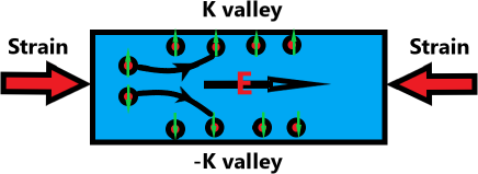
The reduction in dimensionality of 2D materials results in that space inversion symmetry is often eliminated in 2D structures, allowing these materials to become piezoelectricq8 , which is also very important for valleytronics described by Berry curvature . In 2D hexagonal systems with broken space inversion symmetry, the Berry curvature in the K and -K valleys will be nonzero along the out of plane direction, and the Berry curvatures of two valleys are in opposite signs. If the time reversal symmetry is also broken, their absolute values are no longer identical, and the valley contrasting feature will be induced. Under an in-plane longitudinal electric field , the Bloch electrons in these 2D systems will acquire an anomalous Hall velocity due to q9 , and then the anomalous valley Hall effect will be produced, which can be achieved in ferrovalley materialsq10 . Many ferrovalley materials have been predicted, such as 2H-q10 , (X=N and P)q11 , q12 , q13 ; q13-1 , q14 , (X =S and Se)q15 , q16 , q17 . It is a natural idea to induce in-plane longitudinal electric field with an applied uniaxial in-plane strain by piezoelectric effect, and then anomalous valley Hall effect can be produced, which is illustrated in Figure 1.
To well achieve PAVHE, a 2D material should possess the strong FM coupling with PMA (The out-of-plane magnetization easy axis is important not only for FM order but also for valley behavior.), the appropriate energy band gap and valley splitting (The band gap and valley splitting should be large enough to overcome the thermal noise.), and the pure in-plane piezoelectric effect with only (The only independent means only in-plane longitudinal electric field.). Recently, a kind of exotic 2D ferromagnetic semiconductors (X=Cl, Br and I) based on rare-earth ions with f-electrons are predicted to have a large magnetization with high Curie temperature beyond 220 Kg1 ; g2 . The monolayer is predicted as a promising candidate material for valleytronic applications, which is spontaneously valley polarized with a giant splitting of 149 meVg3 . However, possesses in-plane magnetic anisotropy, not PMAg1 ; g2 . Among (X=Cl, Br and I) monolayers, the easy axis of only monolayer is along the out of plane directiong2 . The monolayer has point-group symmetry, which means that only independent is nonzero.
In light of PMA and independent , monolayer is likely to be a potential ferrovalley material to realize PAVHE. In this work, we investigate the valley physics and piezoelectric properties of monolayer by the first-principles calculations. The monolayer exhibits a pair of valleys in the valance band at the K and -K points with a valley splitting of 42.3 meV due to its intrinsic ferromagnetism and SOC. The predicted is -2.708 pm/V, which is comparable to one of -quartz (=2.3 pm/V). To confirm the reliability of our results, the biaxial in-plane strain and electronic correlation effects on valley physics and piezoelectric properties are considered. Finally, the monolayer is predicted to be likely to be a potential ferrovalley material. Our works provide potential 2D valleytronic materials to achieve PAVHE for developing high-performance and controllable valleytronics.




The rest of the paper is organized as follows. In the next section, we shall give our computational details and methods. In the next few sections, we shall present structure and stability, electronic structure and valley Hall effect, and piezoelectric properties of monolayer , along with strain and electronic correlation effects on its valleytronic and piezoelectric properties. Finally, we shall give our discussion and conclusions.
II Computational detail
First-principles calculations with spin-polarization are performed within density functional theory (DFT)1 , as implemented in the Vienna Ab Initio Simulation Package (VASP)pv1 ; pv2 ; pv3 within the projector augmented-wave (PAW) method. The generalized gradient approximation (GGA) in the form of the Perdew-Burke-Ernzerhof (PBE) functional is used as the exchange-correlation interactions. The kinetic energy cutoff is set to 500 eV, and the total energy convergence criterion eV is used. The optimized convergence criterion for atomic coordinates is less than 0.0001 for force on each atom. The vacuum space is set to more than 18 to avoid adjacent interactions. The 18181 Monkhorst-Pack k-point mesh is used to sample the Brillouin zone for calculating electronic structures and elastic properties, and 10201 Monkhorst-Pack k-point mesh for piezoelectric calculations. To account for the localized nature of 4 orbitals of Gd atoms, a Hubbard correction is employed within the rotationally invariant approach proposed by Dudarev et al., where is set as 4 eV, 5 eV, 8 eVg1 ; g2 for for monolayer , and , respectively. The SOC is incorporated for self-consistent energy and band structure calculations. The elastic stiffness tensor are calculated by using strain-stress relationship (SSR) with GGA, and the piezoelectric stress tensor are carried out by density functional perturbation theory (DFPT) methodpv6 with GGA. The 2D elastic coefficients and piezoelectric stress coefficients have been renormalized by = and =, where the is the length of unit cell along z direction. Within finite displacement method, the interatomic force constants (IFCs) of monolayer are calculated based on the 551 supercell with FM ground state. Based on the harmonic IFCs, phonon dispersion spectrum of monolayer is obtained by the Phonopy codepv5 .
III Structure and stability
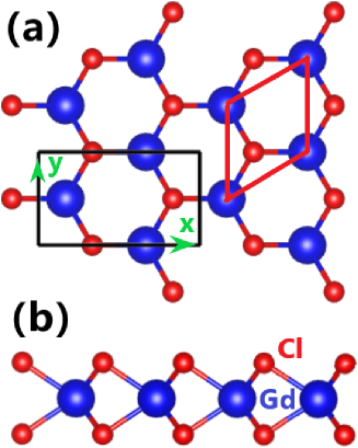
The monolayer belongs to the hexagonal crystal system with 2H- type structure, which contains one Gd atomic layer, sandwiched by two Cl atomic layers (See Figure 2). The corresponding point group is with broken inversion symmetry. The magnetic ground state of monolayer is determined by comparing the energies of antiferromagnetic (AFM) and FM states with rectangle supercell, which is shown in Figure 3. Calculated results show that the FM order is the most stable magnetic state, and the optimized lattice constants with FM order is 3.78 , which is consist with the reported valueg2 . Magnetic anisotropy plays a important role to realize the long-range magnetic ordering in 2D materials, which can be described by magnetic anisotropy energy (MAE). The monolayer and possess in-plane magnetic anisotropyg1 ; g2 . This means that the spin orientations of Gd atoms can be random, and it is difficult to realize the long-range magnetic ordering without external field. However, the easy axis of monolayer is along out of plane directiong2 . By considering SOC interaction, the MAE of monolayer is calculated as the difference between the in-plane and out-of-plane magnetization stability energy, and the corresponding value is 93 /Gd.
The thermal and dynamic stabilities of monolayer have been proved by Ab initio molecular dynamics (AIMD) simulations and phonon dispersiong2 . It is also important to check the mechanical stability of monolayer by calculating elastic constants. Using Voigt notation, the elastic tensor with point-group symmetry for 2D materials can be reduced into:
| (1) |
The calculated results show that and are 45.95 and 13.53 , respectively. The calculated satisfy the Born criteria of mechanical stabilityela : 0 and 0, which confirms the mechanical stability of monolayer . Due to hexagonal symmetry, the monolayer is mechanically isotropic. The 2D Young s moduli , shear modulus and Poisson’s ratios can simply be expressed asela :
| (2) |
| (3) |
| (4) |
The calculate Young’s moduli , shear modulus and Poisson’s ratio are 41.97 , 16.21 and 0.295, respectively. The is less than that of graphene (340 )gra , which indicates that monolayer can be easily tuned by strain, being favorable for novel flexible piezotronics.
IV Electronic structure and valley Hall effect
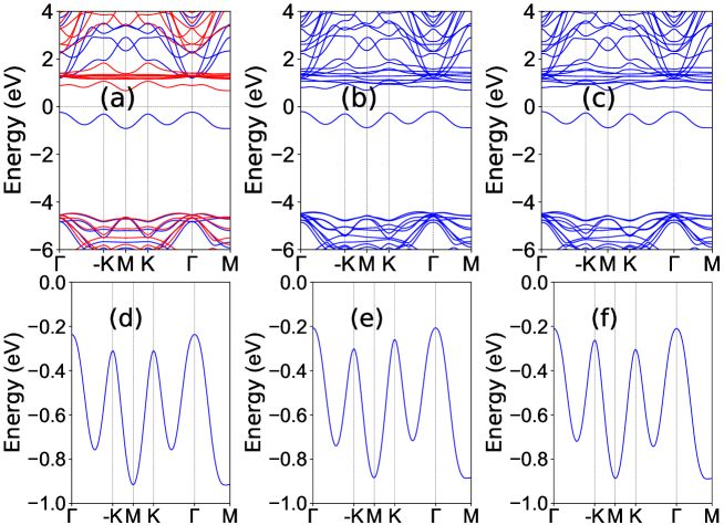
The electronic configuration of isolated Gd atom is . For monolayer , two electrons of one Gd atom are transferred to the six neighboring I atoms, and the electronic configuration of Gd becomes , which will introduce an 8 magnetic moment. The calculated magnetic moment of Gd is 7.463 , and the total magnetic moment per unitcell is 8 . The spin-polarized band structure of monolayer without SOC is shown in Figure 4. The calculated results show that the monolayer is a semiconductors with an indirect band gap of 0.91 eV. The VBM and CBM are provided by the majority spins and minority spins, and they locate at the and M high symmetry points, respectively. This makes monolayer to be a bipolar magnetic semiconductor, which can generate 100 % spin-polarized currents with inverse spin-polarization direction for electron or hole doping. It is clearly seen that the energy extremes of K and -K high-symmetry points are degenerate in the valence band (Figure 4 (d)), and monolayer is a potential ferrovalley material.
The band structures of monolayer with SOC for magnetic moment of Gd along the positive and negative z direction (out of plane) are also plotted in Figure 4. When the SOC is included, the degeneracy between the K and -K valley states is removed in the valence band, and a spontaneous valley polarization is induced with valley splitting of 42.3 meV, which is higher than or compared to ones of reported ferrovalley materials, such as (15 meV)q12 , (33 meV)q13 ; q13-1 , (22 meV)q17 , (49.4 meV)q14 and 2H- (89 meV)q10 . It is found that the energy of K valley state is higher than one of -K valley (Figure 4 (e)). It is interesting that an external magnetic field can tune valley polarization of monolayer . By reversing the magnetization of Gd atoms, the spin and valley polarization can be flipped simultaneously, and the energy of -K valley becomes higher than one of K valley (Figure 4 (f)). These mean that manipulating magnetization direction is an efficient way to tune the valley properties of the monolayer . Furthermore, the band related with valley properties is separated well from other energy bands. Although the VBM of monolayer occurs at point, the K/-K valleys are still well defined and not far in energy. In fact, very small compressive strain (about 1%) can change VBM from to K/-K point (next section). As is well known, the GGA overestimates the lattice constants of materials, and the VBM of monolayer may intrinsically locate at K/-K point.
The combined effects of the intrinsic magnetic exchange field and strong SOC give rise to the spontaneous valley polarization. When the spin polarization is performed without SOC, the spin-up and spin-down states are completely split by the magnetic exchange interaction, but he energy extremes of K and -K high-symmetry points are degenerate in the valence band. When the magnetic exchange interaction is absent, SOC still can induce spin nondegeneracy at both K and -K valley due to missing spatial inversion symmetry, but K and -K valleys are energetically degenerate with opposite spins because of existing time reversal symmetry. In a word, combined with high Curie temperature (224 K)g2 and PMA, is an ideal ferrovalley material for the valleytronic devices.
The valley Hall effect can be described by Berry curvature, and a nonzero Berry curvature along the out of plane direction can be attained in the K and -K valleys for hexagonal systems with broken space inversion symmetry. With the missing time reversal symmetry, the valley contrasting feature can be produced. To study these properties of monolayer , the Berry curvature is calculated directly from the calculated wave functions by using the VASPBERRY code, which is based on Fukui’s methodbm . The calculated Berry curvature distribution of monolayer in the 2D Brillouin zone without SOC and with SOC for magnetic moment of Gd along the positive and negative z direction are shown Figure 5. Without SOC, the Berry curvatures of K and -K valleys are in opposite signs, and the absolute values are the same. When the SOC is included, their absolute values of the Berry curvatures of K and -K valleys are no longer identical, which shows the typical valley contrasting properties. It is also found that the numerical values between K and -K valleys overturn, when the magnetic moment of Gd changes from the positive to negative z direction.
| Name | ||||||
|---|---|---|---|---|---|---|
| 73.87 | 19.61 | 1.365 | -1.048 | 0.317 | 0.584 | |
| 45.95 | 13.53 | 1.028 | -1.906 | -0.878 | -2.708 | |
| 40.46 | 11.68 | 0.847 | -1.742 | -0.895 | -3.110 | |
| 35.49 | 10.09 | 0.658 | -1.356 | -0.698 | -2.748 |
V Piezoelectric properties
The monolayer with point-group symmetry lacks inversion symmetry, but the reflectional symmetry across the xy plane still holds. These mean that only / with defined x and y direction in Figure 2 is nonzero. This is the same with ones of monolayer, but is different from ones of Janus monolayer MoSSe with additional /q7-0 . For 2D materials, only considering the in-plane strain and stressq7-0 ; q7-1 ; q7-2 ; q7-3 ; q7-4 ; q7-5 ; q7-6 ; q7-7 ; q7-8 , the piezoelectric stress and strain tensors by using Voigt notation can be reduced into:
| (5) |
| (6) |
When a uniaxial in-plane strain is imposed, the in-plane piezoelectric polarization (/0) can be induced. However, with an applied biaxial in-plane strain, the in-plane piezoelectric response will be suppressed(/=0). The only independent can be calculated by :
| (7) |
We use the orthorhombic supercell (in Figure 2) to calculate the of monolayer with DFPT method. The calculated is -0.878 C/m with ionic part -1.906 C/m and electronic part 1.028 C/m. The electronic and ionic polarizations have opposite signs, and the ionic contribution dominates the in-plane piezoelectricity. This is different from monolayer , whose electronic and ionic contributions have the same sign, and the electronic part dominates the q7-8 . Based on Equation 7, the can be calculated from previous calculated and . The calculated is -2.708 pm/V, which is comparable to one of -quartz (=2.3 pm/V). The (X= Br and I) monolayers have been predictedg1 ; g2 , and they possess in-plane magnetic anisotropy. Here, we use GGA+ ( = 5.0 and 8.0 eV for monolayer and , respectively) method to investigate piezoelectric properties of (X= Br and I) monolayers. The data related with elastic and piezoelectric properties are summarized in Table 1. It is found that of (X= Br and I) monolayers are comparable with one of .
VI Strain effects
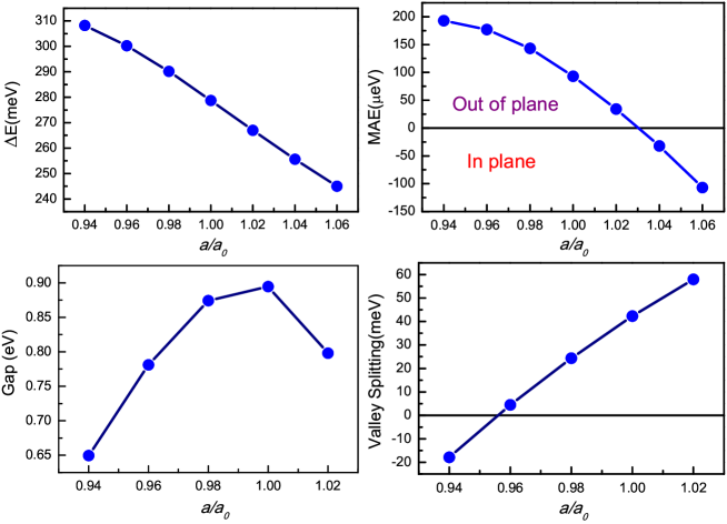
The VBM of unstrained monolayer is at point, and it is necessary to tune VBM to K/-K point by external field for practical applications. As is well known, the strain is a very effective method to tune the electronic structures of 2D materialsc4 ; c5 ; c6 ; c7 ; c8 ; gsd1 ; gsd2 . The is used to simulate the biaxial strain with and being the strained and unstrained lattice constants. In considered strain range, to confirm the FM ground state, the energy differences of AFM with respect to FM state vs with rectangle supercell are plotted in Figure 6. It is fond the energy difference with the biaxial strain varying from 0.94 to 1.06 is always positive, and monotonically decreases. This indicates that the ground state of monolayer is FM in considered strain range, and the strain can strengthen the FM coupling between Gd atoms from tensile strain to compressive one. At applied strain, it is also very important to confirm PMA for stable long-range magnetic ordering without external field. For MAE, Figure 6 shows a decrease with increasing , and the MAE becomes negative value with the strain over 1.03, which means that the easy axis of monolayer turns to in-plane.
We only show energy band structures of monolayer (0.94 to 1.02) with PMA by using GGA+SOC in Figure 7, and the energy band gaps are plotted in Figure 6. At applied strain, monolayer is always an indirect gap semiconductor. It is found that the compressive strain can induce the transition of VBM from point to K/-K point, which can be observed at 0.98 strain. In fact, the change of VBM has been realized at only 0.99 strain, and the corresponding energy band is plotted in FIG.1 of electronic supplementary information (ESI). The tensile strain can make CBM change from M point to one point along -M path. With from 0.94 to 1.02, the energy band gap firstly increases, and then decreases, which can been observed in many 2D materialsgsd1 ; gsd2 . As shown in Figure 6, the valley splitting increases monotonically with the increasing . Conversely, a compressive strain decreases the valley splitting, and the valley splitting will become negative value at about 0.963 strain, which implies that the energy of -K valley is higher than one of K valley. The Berry curvature distributions of monolayer with being 0.94, 0.98 and 1.02 by using GGA+SOC are shown in Figure 8. It is found that the Berry curvatures (absolute value) of two valleys become large with increasing .
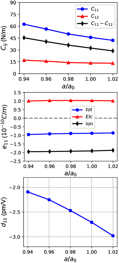
It have been proved that strain engineering can effectively tune piezoelectric properties of 2D materialsr1 ; r2 ; r3 ; r4 , and then we investigate the strain effects on piezoelectric properties of monolayer . The elastic constants (, and -), piezoelectric stress coefficients () along the ionic and electronic contributions, and piezoelectric strain coefficients () of monolayer as a function of are plotted in Figure 9. It is clearly seen that , and - all decrease with increasing strain from 0.94 to 1.02 strain. In the considered strain range, the calculated elastic constants of strained monolayer satisfy the mechanical stability criteriaela , so they are all mechanically stable. It is found that the strain has little effects on , including both the ionic and electronic contributions. However, with increasing , the (absolute value) increases due to reduced - based on Equation 7.
Considering various factors, very small compressive strain (about 0.99 strain) can make monolayer to be a good valley material with PMA, VBM at K/-K point, strong FM coupling, proper valley splitting and to realize PAVHE.
VII electronic correlation effects
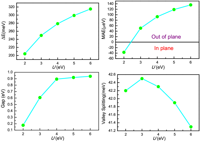
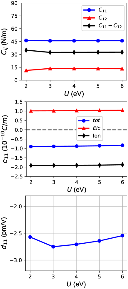
To further confirm the reliability of our results, the electronic correlation effects on magnetic, electronic and piezoelectric properties of monolayer are investigated by choosing different (2-6 eV). The energy differences between AFM and FM states with rectangle supercell and MAE vs are plotted in Figure 10. With increasing , the energy difference is always positive, and monotonically increases. These manifest that the monolayer is always FM order, and the increasing can strengthen the FM coupling between Gd atoms. The MAE shows a decrease with decreasing , and the MAE becomes negative value with easy axis turning to in-plane with being less than about 2.5 eV. The energy band structures of monolayer (=2 to 6 eV) by using GGA+SOC are plotted in FIG.2 of ESI, and the energy band gaps and valley splitting are plotted in Figure 10. When the increases, the VBM is always at K/-K point, and the gap increases. It is found that the electronic correlation has little influence on valley splitting, and the change only 1.2 meV with different (2-6 eV). From FIG.3 of ESI, the electronic correlation has little effects on Berry curvatures of K and -K valleys. The elastic constants (, and -), piezoelectric stress coefficients () along the ionic and electronic contributions, and piezoelectric strain coefficients () of monolayer vs are shown in Figure 11. Calculated results show that electronic correlation has small effects on due to small influence on and , and the change is about 0.21 pm/V.
VIII Discussion and Conclusion
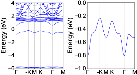
The (X=Cl, Br and I) monolayers have been predictedg1 ; g2 , and the easy axis of monolayer is along the out of plane direction, while monolayer and possess in-plane magnetic anisotropy. When the compressive strain is larger than 3%, the easy axis of monolayer transfers from in-plane to out-of-planeg2 . These mean that monolayer should have PMA due to small atomic radius of F atoms. For monolayer , the energy difference between AFM and FM is 0.285 eV, which means that the FM order is the ground state. The optimized lattice constants is 3.465 , and the calculated and are 73.87 and 19.61 , satisfying the Born criteria of mechanical stabilityela . From FIG.4 of ESI, the monolayer is dynamically stable due to missing imaginary frequency. The PMA of monolayer is confirmed, and the corresponding MAE is 137 eV per Gd atom. The band structures of monolayer with SOC for magnetic moment of Gd along the positive z direction are plotted in Figure 12. The monolayer is a indirect gap semiconductor (0.80 eV) with VBM at K/-K point and CBM at point. It is found that the energy of -K valley is higher than one of K valley with valley splitting of 47.6 meV. Calculated Berry curvature distribution of monolayer with SOC for magnetic moment of Gd along the positive z direction is plotted in FIG.5 of ESI. The absolute values of the Berry curvatures of K and -K valleys are smaller than ones of monolayer , and are no longer identical with the typical valley contrasting properties. Finally, the piezoelectric properties of monolayer are investigated, and the calculated is 0.584 pm/V. With respect to (X=Cl, Br and I) monolayers, the of monolayer becomes positive, which is because the electronic part of monolayer is larger than ionic one. The related data are summarized in Table 1. These results show that monolayer may be a potential valley material to achieve PAVHE.
In summary, a possible way is proposed to achieve anomalous valley Hall effect by piezoelectric effect, and then the valleytronic and piezoelectric properties of monolayer are investigated by the reliable first-principle calculations. Monolayer is a FM semiconductor with a pair of valleys locating at the K and -K points, and possess PMA. Arising from the intrinsic magnetic interaction, broken inversion symmetry and SOC, the valley splitting can be observed between K and -K valleys, and the corresponding value is 42.3 meV. The predicted is -2.708 pm/V, which can provide a suitable in-plane electric field by uniaxial in-plane strain. Moreover, the effects of strain and electronic correlation on the valley physics and piezoelectric properties are also studied. Finally, a 2D FM semiconductor is predicted, which is also a potential ferrovalley material. Our work provides an initial idea for realizing and manipulating the valley physics.
Acknowledgements.
This work is supported by Natural Science Basis Research Plan in Shaanxi Province of China (2021JM-456). We are grateful to the Advanced Analysis and Computation Center of China University of Mining and Technology (CUMT) for the award of CPU hours and WIEN2k/VASP software to accomplish this work.References
- (1) J. R. Schaibley, H. Yu, G. Clark, P. Rivera, J. S. Ross, K. L. Seyler, W. Yao, and X. Xu, Nat. Rev. Mater. 1, 16055 (2016).
- (2) D. Xiao, G. B. Liu, W. Feng, X. Xu, and W. Yao, Phys. Rev. Lett. 108, 196802 (2012).
- (3) S. A. Vitale, D. Nezich, J. O. Varghese, P. Kim, N. Gedik, P. Jarillo-Herrero, D. Xiao, and M. Rothschild, Small 14, 1801483 (2018).
- (4) G. Pacchioni, Nat. Rev. Mater. 5, 480 (2020).
- (5) W. Yao, D. Xiao, and Q. Niu, Phys. Rev. B 77, 235406 (2008).
- (6) D. Xiao, W. Yao, and Q. Niu, Phys. Rev. Lett. 99, 236809 (2007).
- (7) Z. Zhu, A. Collaudin, B. Fauqu, W. Kang, and K. Behnia, Nat. Phys. 8, 89 (2012).
- (8) M. N. Blonsky, H. L. Zhuang, A. K. Singh and R. G. Hennig, ACS Nano, 9, 9885 (2015).
- (9) D. Xiao, M. C. Chang, and Q. Niu, Rev. Mod. Phys. 82, 1959 (2010).
- (10) W. Y. Tong, S. J. Gong, X. Wan, and C. G. Duan, Nat. Commun. 7, 13612 (2016).
- (11) Y. B. Liu, T. Zhang, K. Y. Dou, W. H. Du, R. Peng, Y. Dai, B. B. Huang, and Y. D. Ma, J. Phys. Chem. Lett. 12, 8341 (2021).
- (12) Z. Song, X. Sun, J. Zheng, F. Pan, Y. Hou, M.-H. Yung, J. Yang, and J. Lu, Nanoscale 10, 13986 (2018).
- (13) J. Zhou, Y. P. Feng, and L. Shen, Phys. Rev. B 102, 180407(R) (2020).
- (14) P. Zhao, Y. Ma, C. Lei, H. Wang, B. Huang, and Y. Dai, Appl. Phys. Lett. 115, 261605 (2019).
- (15) X. Y. Feng, X. L. Xu, Z. L. He, R. Peng, Y. Dai, B. B. Huang and Y. D. Ma, Phys. Rev. B 104, 075421 (2021)
- (16) Y. Zang, Y. Ma, R. Peng, H. Wang, B. Huang, and Y. Dai, Nano Res. 14, 834 (2021).
- (17) R. Peng, Y. Ma, X. Xu, Z. He, B. Huang, and Y. Dai, Phys. Rev. B 102, 035412 (2020).
- (18) W. Du, Y. Ma, R. Peng, H. Wang, B. Huang, and Y. Dai, J. Mater. Chem. C 8, 13220 (2020).
- (19) B. Wang, X. W. Zhang, Y. H. Zhang, S. J. Yuan, Y. L. Guo, S. Dong and J. L. Wang, Mater. Horiz. 7, 1623 (2020).
- (20) W. Q. Liu, J. W. Tong, L. Deng, B. Yang, G. M. Xie, G. W. Qin, F. B. Tian, X. M. Zhang, Materials Today Physics 21, 100514 (2021).
- (21) H. X. Cheng, J. Zhou, W. Ji, Y. N. Zhang and Y. P. Feng, Phys. Rev. B 103, 125121 (2021).
- (22) P. Hohenberg and W. Kohn, Phys. Rev. 136, B864 (1964); W. Kohn and L. J. Sham, Phys. Rev. 140, A1133 (1965).
- (23) G. Kresse, J. Non-Cryst. Solids 193, 222 (1995).
- (24) G. Kresse and J. Furthmller, Comput. Mater. Sci. 6, 15 (1996).
- (25) G. Kresse and D. Joubert, Phys. Rev. B 59, 1758 (1999).
- (26) J. P. Perdew, K. Burke and M. Ernzerhof, Phys. Rev. Lett. 77, 3865 (1996).
- (27) X. Wu, D. Vanderbilt and D. R. Hamann, Phys. Rev. B 72, 035105 (2005).
- (28) A. Togo, F. Oba, and I. Tanaka, Phys. Rev. B 78, 134106 (2008).
- (29) E. Cadelano and L. Colombo, Phys. Rev. B 85, 245434 (2012).
- (30) C. Lee, X. Wei, J. W. Kysar and J. Hone, Science 321, 385 (2008).
- (31) T. Fukui, Y. Hatsugai and H. Suzuki, J. Phys. Soc. Japan. 74, 1674 (2005).
- (32) L. Dong, J. Lou and V. B. Shenoy, ACS Nano, 11, 8242 (2017).
- (33) R. X. Fei, We. B. Li, J. Li and L. Yang, Appl. Phys. Lett. 107, 173104 (2015).
- (34) M. N. Blonsky, H. L. Zhuang, A. K. Singh and R. G. Hennig, ACS Nano, 9, 9885 (2015).
- (35) Y. Chen, J. Y. Liu, J. B. Yu, Y. G. Guo and Q. Sun, Phys. Chem. Chem. Phys. 21, 1207 (2019).
- (36) S. D. Guo, Y. T. Zhu, W. Q. Mu and W. C. Ren, EPL 132, 57002 (2020).
- (37) S. D. Guo, Y. T. Zhu, W. Q. Mu, L. Wang and X. Q. Chen, Comp. Mater. Sci. 188, 110223 (2021).
- (38) Y. Guo, S. Zhou, Y. Z. Bai, and J. J. Zhao, Appl. Phys. Lett. 110, 163102 (2017).
- (39) W. B. Li and J. Li, Nano Res. 8, 3796 (2015).
- (40) K. N. Duerloo, M. T. Ong and E. J. Reed, J. Phys. Chem. Lett. 3, 2871 (2012).
- (41) K. L. He, C. Poole, K. F. Mak and J. Shan, Nano Lett. 13, 2931 (2013).
- (42) H. L. Shi, H. Pan, Y. W. Zhang and B. I. Yakobson, Phys. Rev. B 87, 155304 (2013).
- (43) T. Cheiwchanchamnangij, W. R. L. Lambrecht, Y. Song and H. Dery, Phys. Rev. B 88, 155404 (2013).
- (44) H. Y. Lv, W. J. Lu, D. F. Shao, H. Y. Lub and Y. P. Sun, J. Mater. Chem. C 4, 4538 (2016).
- (45) H. Peelaers and C. G. Van de Walle, Phys. Rev. B 86, 241401(R) (2012).
- (46) S. D. Guo and J. Dong, Semicond. Sci. Tech. 33, 085003 (2018).
- (47) S. D. Guo, J. Mater. Chem. C 4, 9366 (2016).
- (48) N. Jena, Dimple, S. D. Behere and A. D. Sarkar, J. Phys. Chem. C 121, 9181 (2017).
- (49) S. D. Guo, X. S. Guo, Y. Y. Zhang and K. Luo, J. Alloy. Compd. 822, 153577 (2020).
- (50) Dimple, N. Jena, A. Rawat, R. Ahammed, M. K. Mohanta and A. D. Sarkar, J. Mater. Chem. A 6, 24885 (2018).
- (51) S. D. Guo, W. Q. Mu and Y. T. Zhu, J. Phys. Chem. Solids 151, 109896 (2021).