An Integrated Quantum Material Testbed with Multi-Resolution Photoemission Spectroscopy
Abstract
We present the development of a multi-resolution photoemission spectroscopy (MRPES) setup which probes quantum materials in energy, momentum, space, and time. This versatile setup integrates three light sources in one photoemission setup, and can conveniently switch between traditional angle-resolved photoemission spectroscopy (ARPES), time-resolved ARPES (trARPES), and micron-scale spatially resolved ARPES (ARPES). It provides a first-time all-in-one solution to achieve an energy resolution meV, a time resolution fs, and a spatial resolution m in photoemission spectroscopy. Remarkably, we obtain the shortest time resolution among the trARPES setups using solid-state nonlinear crystals for frequency upconversion. Furthermore, this MRPES setup is integrated with a shadow-mask assisted molecular beam epitaxy system, which transforms the traditional photoemission spectroscopy into a quantum device characterization instrument. We demonstrate the functionalities of this novel quantum material testbed using FeSe/SrTiO3 thin films and MnBi4Te7 magnetic topological insulators.
I Introduction
Angle-resolved photoemission spectroscopy (ARPES) has been established as a powerful tool to directly reveal the single-particle spectral function , which encodes electronic band structures and many-body interactions Damascelli, Hussain, and Shen (2003); Sobota, He, and Shen (2021). ARPES has played a major role in the discovery of the -wave superconducting gap in cuprate superconductors Shen et al. (1993); Vishik et al. (2012), the Dirac surface state in topological insulators Hsieh et al. (2008); Chen et al. (2009), and recently the putative topological superconducting gap in FeTe0.55Se0.45. Zhang et al. (2018)
Investigations on quantum materials often require the combination of different modalities in photoemission spectroscopy. Current solutions for multi-modal ARPES rely on the utilization of facilities at different geographical locations. For instance, one may use a laboratory-based ARPES setup to measure superconducting gaps in monolayer FeSe/SrTiO3, Liu et al. (2012); Tan et al. (2013); He et al. (2013) but will need micro ()- Iwasawa et al. (2017) or nanoARPES Barbo et al. (2000); Avila et al. (2013); Rotenberg and Bostwick (2014) at specialized synchrotron end stations to understand the microscopic spatial variations Faeth et al. (2021). One may use a time-resolved ARPES (trARPES) setup Perfetti et al. (2007); Schmitt et al. (2008); Sobota et al. (2012); Smallwood et al. (2012); Wang et al. (2013); Yang et al. (2015a); Gerber et al. (2017) to resolve the dynamics of unoccupied electronic states in a topological insulator Bi2Se3 Sobota et al. (2012, 2013), but will need high-photon-energy synchrotron-based measurements to reveal the valence band dispersions Soifer et al. (2019). Importantly, multi-modal ARPES measurements are remarkably challenging due to the limited access to multiple facilities and the potential sample degradations during transportation.
It is thus demanded to integrate multiple modalities in one ARPES setup. This integration brings fundamental challenges if using a single light source. For instance, the energy and temporal widths of light pulses are conjugate quantities dictated by the fundamental uncertainty principle Gauthier et al. (2020). A sub-100-fs time resolution in trARPES is concomitant with an energy resolution meV in static ARPES. Moreover, micron or sub-micron-sized beam spots in ARPES or nanoARPES can lead to a significant space-charging effect which is detrimental in high-energy-resolution applications. This problem is particularly severe for photon energies > 10 eV. Rotenberg and Bostwick (2014); He et al. (2016)
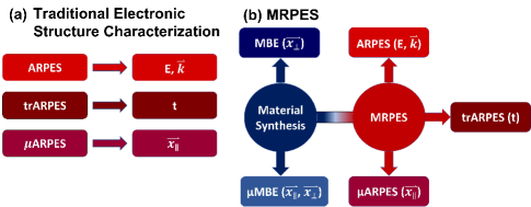
In this report, we present a new integrated platform for multi-resolution photoemission spectroscopy (MRPES). This MRPES setup integrates a Helium discharge lamp, a narrow bandwidth 6 eV laser, and a tunable ultrafast laser, which effectively combines static ARPES, trARPES, and ARPES. This setup provides a first-time all-in-one solution for multi-modal photoemission spectroscopy (Fig. 1(b)). From calibration experiments on Bi2Se3 and MnBi2Te4 we demonstrate an energy resolution meV in static laser-based ARPES, a time resolution of fs in trARPES, and a spatial resolution of m in ARPES. Remarkably, our time resolution sets a new record for trARPES setups with probe pulses generated by solid-state nonlinear crystals. In connection with a molecular beam epitaxy (MBE) system incorporating shadow masks, our setup enables a holistic probing of quantum materials which are engineered both in-plane and out-of-plane. The MRPES setup combines complementary capabilities of low and high photon energies, of energy and time resolutions, and of spatial and momentum probes. We demonstrate the performance of this novel setup using FeSe/SrTiO3 thin film superconductors and MnBi4Te7 magnetic topological insulators.
II Experimental Setup
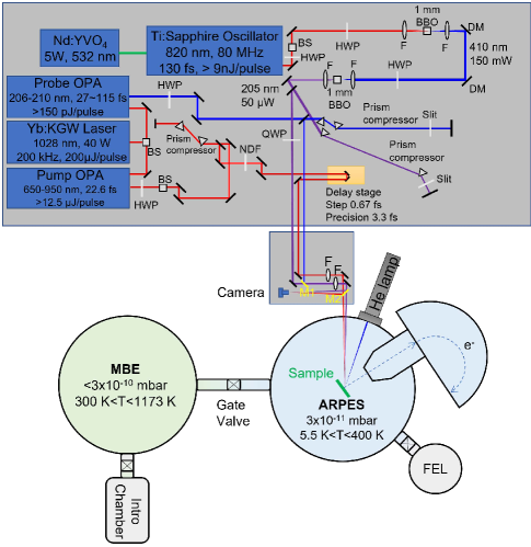
The MRPES platform is schematically illustrated in Fig. 2. Multiple light sources are connected to the photoemission chamber. The first light source is a 6 eV beam operating at a repetition rate of 80 MHz. A mode locked Ti:Sapphire oscillator (Coherent MIRA Optima 900) is pumped by a W continuous wave seed laser (Coherent Verdi V5). The Ti:Sapphire oscillator is tunable between and nm, and is typically set at nm with nJ pulse energies. nm pulses pass through two stages of second harmonic generation using -barium borate (BBO) crystals to yield the fourth harmonic (205 nm) used for photoemission. The fourth harmonic is separated by a prism-pair compressor. A quarter waveplate (QWP) is used to switch between linear and circular polarizations.
The second light source is optimized for trARPES and begins with a diode-pumped Yb:KGW laser (Light Conversion Carbide C3). The laser outputs J, fs pulses with a central wavelength at nm and a repetition rate of kHz. This beam is split by a polarizing beam splitter and sent into two non-collinear optical parametric amplifiers (OPAs). J are sent into a pump OPA to generate a tunable signal beam between 650 nm and 950 nm, and is typically set at 800 nm. The output pulses have a pulse duration of fs and a pulse energy J. The pump beam is directed to a delay stage which varies the beam path length by up to 30 cm (1 ns).
The remaining J from Carbide are sent to the probe OPA where J of signal at nm is generated. J of the second harmonic ( nm) and pJ of the fourth harmonic ( nm) are obtained using BBO crystals built into the probe OPA. The pulse duration of the nm beam varies between and fs, which is tuned by the thicknesses of the BBO crystals Gauthier et al. (2020). A prism-pair compressor compensates for the group velocity dispersion (GVD) and controls the bandwidth of the nm beam. The addition of a remountable mirror M1 switches between the eV beams from the Ti:Sapphire oscillator and from the probe OPA. The remountable mirror M2 can be used to route both the pump and probe beams to a profiling camera where the spatial overlap is established.
The final light source is a Helium discharge lamp (Scienta VUV5000) which is integrated into the MRPES system in vacuo. A grating-based monochromator can switch between the He (21.2 eV), He (23.1 eV), or He (40.8 eV) lines allowing access to full Brillouin zones of most materials, which cannot be accomplished using 6 eV beams.
Integrating three light sources in the MRPES system realizes complementary functionalities. For instance, high photon energies from the Helium discharge lamp reveal the entirety of a Brillouin zone, while the Ti:Sapphire-based 6 eV laser provides a surgical, ultrahigh energy-resolution probe of the band structure near the zone center. With an 80 MHz repetition rate, the Ti:Sapphire-based 6 eV laser minimizes the space-charging effect Corder et al. (2018), and is an ideal source to optimize energy and spatial resolutions. The 200 kHz Yb:KGW system in combination with the non-collinear OPA’s is an ideal light source for ultrafast trARPES measurements.
The heart of the MRPES system is a hemispherical electron analyzer (Scienta DA30-L). The featured deflection voltage enables measurements of electrons emitted up to 15 deg with respect to the surface normal, which leads to convenient band mapping in a limited momentum range without the need to rotate samples. This is particularly important for precise measurements of micron-scale domains. Samples are loaded into a 6-axis manipulator reaching K with liquid Helium. The measurement chamber pressure is at mbar when the manipulator is at room temperature, and drops to mbar at the base temperature. This excellent vacuum condition leads to an extended sample lifetime days as characterized by photoemission experiments.
The MRPES system is connected under ultrahigh vacuum (UHV) to the MBE growth chamber which has a base pressure of 3 10-10 mbar. Substrates can be loaded into MBE separately from the ARPES system through an introduction chamber. The MBE system features up to seven effusion cells, as well as a manipulator providing radiative heating up to C or direct current heating up to C. Notably, we implement laser-cut stainless-steel shadow masks to perform patterned growth. This shadow mask technique allows us to print micron-scale patterns without the need of exposing thin films to ambient or harsh environments for lithographic processing Zhou et al. (2003); Tsioutsios et al. (2020) and is thus termed MBE. The printing resolution is currently limited by the laser cutting precision m. In combination with ARPES, our system enables a new modality to perform microscopic synthesis and characterization on novel quantum materials. A proof-of-principle experiment is shown in Fig. 4.
III MRPES Calibration
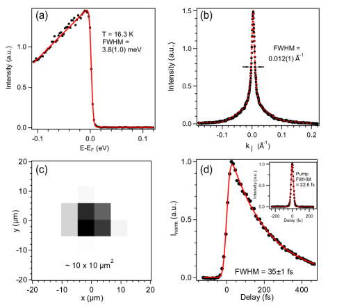
Our best energy resolution is realized by the 80 MHz Ti:Sapphire based beamline. We characterize the overall energy resolution using an exemplary measurement on a cleaved single-crystal Bi2Se3 at K. Figure 3(a) shows an energy distribution curve (EDC) taken through the point near the Fermi level (E). The EDC was fit to a a modified Fermi-Dirac (FD) function, where the original FD distribution is multiplied with a linear density-of-states function and convolved with a Gaussian resolution function. The energy resolution, meV, is close to the theoretical best overall energy resolution of meV. This theoretical estimate is based on the analyzer resolution of meV and the eV laser bandwidth of meV. Gauthier et al. (2020)
While it is difficult to characterize our momentum resolution, we present an upper limit by showing a momentum distribution curve (MDC) taken at the Dirac point of an antiferromagnetic topological insulator MnBi2Te4 (Fig. 3(b)). The Ti:Sapphire oscillator is again used for this characterization. The full width at half maximum (FWHM) is determined to be Å-1 by fitting the MDC to a Lorentzian function. We emphasize that this width is limited by material physics and only provides an upper limit for the momentum resolution.
The spatial resolution of the ARPES module is characterized by imaging the focused beam profile. In a typical setup, the beam is first expanded to a diameter of mm, and then focused by a lens with a focal length of mm. The theoretical diffraction limited FWHM at the focal point is m. Wolfgang (2014) The high repetition rate Corder et al. (2018) and low photon energy Zhou et al. (2005) both lead to a minimal space charging effect. Figure 3(c) shows an image of the focused beam profile using an Imaging Source DMK 23U618 camera. Even though we cannot extract the exact FWHM’s of the beam profile due to the m pixel size, we determine that the central four pixels occupy % of the total integrated intensity. Notably, for a Gaussian beam, the integrated intensity within the central region defined by FWHM’s occupies % of the total integrated intensity. Hence we estimate the beam size to be m2. Importantly, the projected horizontal beam waist will be enlarged by a factor of where is the laser’s angle of incidence.
We demonstrate the time resolution of the trARPES module using the 200 kHz ultrafast pump-probe setup. Prism-pair compressors compensate for any broadening due to the group velocity dispersion (GVD) in both pump and probe pulses. We perform a trARPES experiment on a Bi2Se3 sample with a pump fluence of J/cm2. A cross-correlation is extracted from 1 eV above E and is fitted to an exponential function convolved with a Gaussian resolution function (Figure 3(d)). The fitting yields a FWHM = fs, which is to our knowledge the best time resolution among all trARPES setups using solid-crystal-based frequency upconversion Gauthier et al. (2020); Ishida et al. (2014); Yang et al. (2019); Sobota et al. (2012); Graf et al. (2011); Wang et al. (2012a); Perfetti et al. (2007). This time resolution is obtained using a m-thick BBO for second harmonic generation (SHG), and a m-thick BBO for fourth harmonic generation (FHG). Since our pump pulse duration is fs (inset of Fig. 3(d)), the FWHM duration of the probe pulse is determined to be fs. By utilizing a m-thick SHG BBO and a m-thick FHG BBO, and retuning the probe compressor, we can also obtain an energy resolution of meV and a time resolution of fs. The high-time-resolution and high-energy-resolution setups allow us to reveal sub-50 fs dynamics and sub-20 meV energy features, respectively.
IV Material Application
To demonstrate the multi-modalities of the MRPES system, we present studies on FeSe/SrTiO3 thin film superconductors and MnBi4Te7 antiferromagnetic topological insulators. As demonstrated below, MRPES resolves fine features of FeSe/SrTiO3 in both the energy and time domains, and disentangles termination-dependent topological properties of MnBi4Te7.
IV.1 FeSe
FeSe/SrTiO3 thin film superconductors Wang et al. (2012b); Lee et al. (2014); Song et al. (2019); Yang et al. (2015b); Gerber et al. (2017); Suzuki et al. (2019) are model systems where the key electronic interactions occur at multiple energy scales. A strong coupling between the FeSe electrons and the meV SrTiO3 phonons leads to a substantial boost of the superconducting gap in monolayer FeSe/SrTiO3. Lee et al. (2014); Song et al. (2019) Cooperative electron-electron and electron-phonon interactions yields an orders-of-magnitude enhancement to the coupling with the meV Se A1g mode Yang et al. (2015b); Gerber et al. (2017); Suzuki et al. (2019). Resolving these different interactions on a single sample necessitates the usage of the MRPES setup. We grow an -unit-cell thick (-UC) FeSe thin film using the MBE module following recipes in the literature Lee et al. (2014); Faeth et al. (2021) and transfer the sample in vacuo to the MRPES module for multi-resolution measurements.
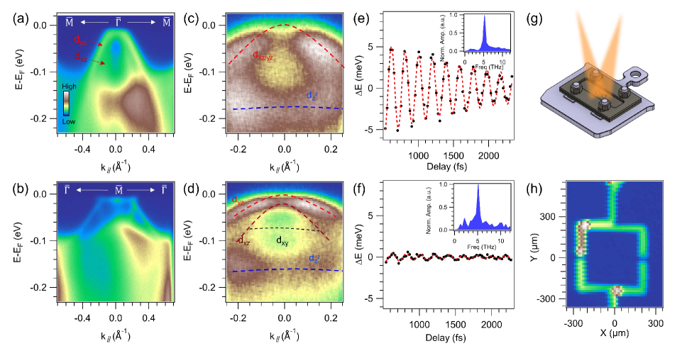
Traditional ARPES measurements based on the Helium discharge lamp are first conducted to resolve the electronic band structure across the entire Brillouin zone. Photoemission spectra taken at K near the and points are shown in Fig. 4(a) and 4(b), respectively. Two distinct hole-like bands are resolved near , which are attributed to the and orbitals. Near the point a complex electronic band structure involving at least two electron-like and one hole-like pockets is resolved, which is due to the nematic splitting of all three orbitals Zhang et al. (2016); Yi et al. (2019). These findings agree with those in the literature Zhang et al. (2016); Yi et al. (2019); Tan et al. (2013), and establish the high quality of our thin films.
To understand the key electronic interactions, we perform trARPES using both the high-time-resolution setup where the time and energy resolutions are fs and meV, as well as a high-energy-resolution setup where the time and energy resolutions are fs and meV. The pump fluence is maintained at mJ/cm2 and the manipulator temperature is kept at K. Notably, the and orbitals cannot be separately resolved in trARPES due to finite energy resolutions, and we denote the overlapping spectral feature as the band.
We extract the time-dependent band shift of the band by fitting the EDCs to a 2-band model Gerber et al. (2017). The non-oscillatory component of the band shift dynamics is approximated using a 7th-order polynomial. We obtain the oscillation amplitude by fitting the oscillatory component to a cosine function modulated by an exponential decay. For the high-time-resolution setup (Fig. 4(c)), a prominent oscillation near THz is observed with an amplitude of 7.95 meV at time zero, which is attributed to the Se A1g mode Yang et al. (2015b); Gerber et al. (2017); Suzuki et al. (2019). In contrast, using the high-energy-resolution setup (Fig. 4(d)) we resolve oscillations with an amplitude of only 0.73 meV at time zero. The reduction of the oscillation amplitude in the latter measurement results from the convolution with the 115 fs time resolution Gerber et al. (2017). This difference clearly demonstrates the advantage of the high-time-resolution setup in resolving fine features in the time domain.
The benefits of the high-energy-resolution setup can be seen in the energy domain (Fig. 4(d)). With a meV energy resolution, trARPES not only resolves overall sharper band dispersions, but more importantly allows the identification of the weak band. This band is of particular interest as it undergoes an orbital selective Mott transition at high temperatures Huang et al. (2021).
In addition to characterizing materials, the MRPES platform allows for micro-fabrication and micro-characterization based on the MBE and ARPES modules. In MBE we grow a patterned 4-UC FeSe/SrTiO3 film using a shadow mask (Fig. 4(g)). A m thick, stainless steel shadow mask is sandwiched between two Tantalum spacers and placed at 0.4 mm over an annealed SrTiO3 substrate. The substrate-mask system is loaded into the MBE chamber and exposed to molecular beams. As a system test, we select a mask that features a square ring pattern with a 50 m linewidth and a 20 m gap between the upper and lower halves. The device quality is characterized using the ARPES module. The ARPES mapping based on overall photoemission counts on the detector (Fig. 4(h)) reveals the targeted m linewidth and m gaps. Higher intensities on the left side are most likely due to the alignment between effusion cells and the shadow mask. A thinner shadow mask possibly made of Si3N4 and a shorter mask-substrate distance will improve the printing resolution down to nm. Zhou et al. (2003); Tsioutsios et al. (2020); Grévin et al. (2011)
IV.2 MnBi4Te7
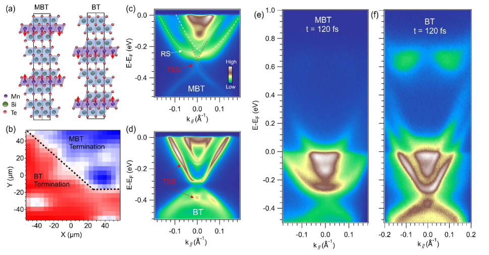
The need for a multi-resolution approach to photoemission characterization can also be seen in MnBi4Te7. MnBi4Te7 is an antiferromagnetic topological insulator which consists of alternating septuple layers of MnBi2Te4 (MBT) and quintuple layers of Bi2Te3 (BT) Hu et al. (2020a); Vidal et al. (2021); Wu et al. (2020); Hu et al. (2020b). As such, there are two possible terminations when a MnBi4Te7 sample is cleaved (Fig. 5(a)). Domains of each termination are on the order of tens of m with sharp boundaries, making it crucial to employ a microscopic beam size to ensure probing of single domains.
We first perform a spatial map of MnBi4Te7 at room temperature (Fig. 5(b)). The spatial map shows a clear distinction between adjacent MBT and BT domains. Measurements at K at selected MBT and BT locations provide a detailed view of the band structures (Fig. 5(c) and 5(d)). While the focus of this work is on the technical capabilities of MRPES, we note that the interpretations of various spectral features from MnBi4Te7 are currently under debates Hu et al. (2020a); Vidal et al. (2021); Ma et al. (2020). Based on our previous studies Yan et al. (2021a, b), we attribute the large electron-like pocket on the MBT termination to a pair of Rashba-split states. On the BT termination, the topological surface state (TSS) hybridizes with the valence bands, resulting in the Dirac point located near -0.38 eV.
We also perform trARPES to reveal the unoccupied band structure. ARPES spectra near are obtained at 120 fs on both terminations (Fig. 5(e) and 5(f)) using the high-energy-resolution ultrafast setup. The unoccupied parts of the conduction bands and TSS’s are resolved up to eV above for both terminations. On the BT termination, additional features near eV are resolved. These high-energy features are results of direct optical transitions, and serve as an electron reservoir to fill the low-energy states Sobota et al. (2012). Obtaining information about both the occupied and unoccupied band structures is crucial for a complete analysis of the material and showcases the necessity of employing a multi-resolution system.
V Conclusion
We have presented a MRPES platform that integrates helium lamp ARPES, static laser ARPES, trARPES, ARPES, MBE, and MBE into one system. The demonstrated energy resolution of meV for static ARPES, time resolution of fs for trARPES, and spatial resolution of m for ARPES allow for a holistic probing of materials’ electronic properties. Our time resolution is the fastest among all trARPES setups using solid-crystal frequency upconversion. The integration with MBE and MBE further enables material engineering both in- and out-of-plane, and opens the door to in situ device fabrication. The performance of the MRPES system is benchmarked by the studies on thin film superconductors FeSe/SrTiO3 and antiferromagnetic topological insulators MnBi4Te7.
We emphasize that MRPES is not merely a combination of different ARPES modules. The simultaneous probing into energy, momentum, space and time, with uncompromised resolutions in each domain, allows us to fully reveal the complex physics in novel quantum materials. The adaptability and level of control unlock the ability to create and understand quantum devices such as superconducting qubits and superconducting quantum interference devices (SQUIDs) which transcends the traditional ARPES tool into a multi-modality quantum device characterization instrument.
Acknowledgements.
This work is partially supported by NSF grant #2019131. E.G. acknowledges support by the UChicago Dean’s Scholars program. R.F. acknowledges support by the UChicago Jeff Metcalf program. The MnBi4Te7 sample preparation was supported by the National Science Foundation through the Penn State 2D Crystal Consortium-Materials Innovation Platform (2DCC-MIP) under NSF cooperative agreement DMR-1539916. We would like to thank Jonathan Sobota, Patrick Kirchmann, Hadas Soifer, Alexandre Gauthier, Brendan Faeth, Kyle Shen, Darrell Schlom, and David Awschalom for helpful discussions. The authors have no conflicts to disclose.Data Availability
The data that support the findings of this study are available from the corresponding author upon reasonable request.
References
- Damascelli, Hussain, and Shen (2003) A. Damascelli, Z. Hussain, and Z.-X. Shen, “Angle-resolved photoemission studies of the cuprate superconductors,” Reviews of Modern Physics 75, 473–541 (2003).
- Sobota, He, and Shen (2021) J. A. Sobota, Y. He, and Z.-X. Shen, “Angle-resolved photoemission studies of quantum materials,” Reviews of Modern Physics 93, 025006 (2021).
- Shen et al. (1993) Z.-X. Shen, D. S. Dessau, B. O. Wells, D. M. King, W. E. Spicer, A. J. Arko, D. Marshall, L. W. Lombardo, A. Kapitulnik, P. Dickinson, S. Doniach, J. DiCarlo, T. Loeser, and C. H. Park, “Anomalously large gap anisotropy in the a-b plane of Bi2Sr2CaCu2O8+δ,” Physical Review Letters 70, 1553–1556 (1993).
- Vishik et al. (2012) I. M. Vishik, M. Hashimoto, R.-H. He, W.-S. Lee, F. Schmitt, D. Lu, R. G. Moore, C. Zhang, W. Meevasana, T. Sasagawa, S. Uchida, K. Fujita, S. Ishida, M. Ishikado, Y. Yoshida, H. Eisaki, Z. Hussain, T. P. Devereaux, and Z.-X. Shen, “Phase competition in trisected superconducting dome,” Proceedings of the National Academy of Sciences 109, 18332–18337 (2012).
- Hsieh et al. (2008) D. Hsieh, D. Qian, L. Wray, Y. Xia, Y. S. Hor, R. J. Cava, and M. Z. Hasan, “A topological Dirac insulator in a quantum spin Hall phase,” Nature 452, 970–974 (2008).
- Chen et al. (2009) Y. L. Chen, J. G. Analytis, J.-H. Chu, Z. K. Liu, S.-K. Mo, X. L. Qi, H. J. Zhang, D. H. Lu, X. Dai, Z. Fang, S. C. Zhang, I. R. Fisher, Z. Hussain, and Z.-X. Shen, “Experimental realization of a three-dimensional topological insulator, Bi2Te3,” Science (2009).
- Zhang et al. (2018) P. Zhang, K. Yaji, T. Hashimoto, Y. Ota, T. Kondo, K. Okazaki, Z. Wang, J. Wen, G. D. Gu, H. Ding, and S. Shin, “Observation of topological superconductivity on the surface of an iron-based superconductor,” Science (2018).
- Liu et al. (2012) D. Liu, W. Zhang, D. Mou, J. He, Y.-B. Ou, Q.-Y. Wang, Z. Li, L. Wang, L. Zhao, S. He, Y. Peng, X. Liu, C. Chen, L. Yu, G. Liu, X. Dong, J. Zhang, C. Chen, Z. Xu, J. Hu, X. Chen, X. Ma, Q. Xue, and X. J. Zhou, “Electronic origin of high-temperature superconductivity in single-layer FeSe superconductor,” Nature Communications 3, 931 (2012).
- Tan et al. (2013) S. Tan, Y. Zhang, M. Xia, Z. Ye, F. Chen, X. Xie, R. Peng, D. Xu, Q. Fan, H. Xu, J. Jiang, T. Zhang, X. Lai, T. Xiang, J. Hu, B. Xie, and D. Feng, “Interface-induced superconductivity and strain-dependent spin density waves in FeSe/SrTiO3 thin films,” Nature Materials 12, 634–640 (2013).
- He et al. (2013) S. He, J. He, W. Zhang, L. Zhao, D. Liu, X. Liu, D. Mou, Y.-B. Ou, Q.-Y. Wang, Z. Li, L. Wang, Y. Peng, Y. Liu, C. Chen, L. Yu, G. Liu, X. Dong, J. Zhang, C. Chen, Z. Xu, X. Chen, X. Ma, Q. Xue, and X. J. Zhou, “Phase diagram and electronic indication of high-temperature superconductivity at 65 K in single-layer FeSe films,” Nature Materials 12, 605–610 (2013).
- Iwasawa et al. (2017) H. Iwasawa, E. F. Schwier, M. Arita, A. Ino, H. Namatame, M. Taniguchi, Y. Aiura, and K. Shimada, “Development of laser-based scanning µ-ARPES system with ultimate energy and momentum resolutions,” Ultramicroscopy 182, 85–91 (2017).
- Barbo et al. (2000) F. Barbo, M. Bertolo, A. Bianco, G. Cautero, S. Fontana, T. K. Johal, S. La Rosa, G. Margaritondo, and K. Kaznacheyev, “Spectromicroscopy beamline at ELETTRA: Performances achieved at the end of commissioning,” Review of Scientific Instruments 71, 5–10 (2000).
- Avila et al. (2013) J. Avila, I. Razado-Colambo, S. Lorcy, J.-L. Giorgetta, F. Polack, and M. C. Asensio, “Interferometer-controlled soft X-ray scanning photoemission microscope at SOLEIL,” Journal of Physics: Conference Series 425, 132013 (2013).
- Rotenberg and Bostwick (2014) E. Rotenberg and A. Bostwick, “MicroARPES and nanoARPES at diffraction-limited light sources: Opportunities and performance gains,” Journal of Synchrotron Radiation 21, 1048–1056 (2014).
- Faeth et al. (2021) B. Faeth, S.-L. Yang, J. Kawasaki, J. Nelson, P. Mishra, C. Parzyck, C. Li, D. Schlom, and K. Shen, “Incoherent Cooper pairing and pseudogap behavior in single-layer FeSe/SrTiO3,” Physical Review X 11, 021054 (2021).
- Perfetti et al. (2007) L. Perfetti, P. A. Loukakos, M. Lisowski, U. Bovensiepen, H. Eisaki, and M. Wolf, “Ultrafast electron relaxation in superconducting Bi2Sr2CaCu2O8+δ by time-resolved photoelectron spectroscopy,” Physical Review Letters 99, 197001 (2007).
- Schmitt et al. (2008) F. Schmitt, P. S. Kirchmann, U. Bovensiepen, R. G. Moore, L. Rettig, M. Krenz, J.-H. Chu, N. Ru, L. Perfetti, D. H. Lu, M. Wolf, I. R. Fisher, and Z.-X. Shen, “Transient electronic structure and melting of a charge density wave in TbTe3,” Science (2008).
- Sobota et al. (2012) J. A. Sobota, S. Yang, J. G. Analytis, Y. L. Chen, I. R. Fisher, P. S. Kirchmann, and Z.-X. Shen, “Ultrafast optical excitation of a persistent surface-state population in the topological insulator Bi2Se3,” Physical Review Letters 108, 117403 (2012).
- Smallwood et al. (2012) C. L. Smallwood, J. P. Hinton, C. Jozwiak, W. Zhang, J. D. Koralek, H. Eisaki, D.-H. Lee, J. Orenstein, and A. Lanzara, “Tracking Cooper pairs in a cuprate superconductor by ultrafast angle-resolved photoemission,” Science (2012).
- Wang et al. (2013) Y. H. Wang, H. Steinberg, P. Jarillo-Herrero, and N. Gedik, “Observation of Floquet-Bloch states on the surface of a topological insulator,” Science (2013).
- Yang et al. (2015a) S.-L. Yang, J. Sobota, D. Leuenberger, Y. He, M. Hashimoto, D. Lu, H. Eisaki, P. Kirchmann, and Z.-X. Shen, “Inequivalence of single-particle and population lifetimes in a cuprate superconductor,” Physical Review Letters 114, 247001 (2015a).
- Gerber et al. (2017) S. Gerber, S.-L. Yang, D. Zhu, H. Soifer, J. A. Sobota, S. Rebec, J. J. Lee, T. Jia, B. Moritz, C. Jia, A. Gauthier, Y. Li, D. Leuenberger, Y. Zhang, L. Chaix, W. Li, H. Jang, J.-S. Lee, M. Yi, G. L. Dakovski, S. Song, J. M. Glownia, S. Nelson, K. W. Kim, Y.-D. Chuang, Z. Hussain, R. G. Moore, T. P. Devereaux, W.-S. Lee, P. S. Kirchmann, and Z.-X. Shen, “Femtosecond electron-phonon lock-in by photoemission and X-ray free-electron laser,” Science 357, 71–75 (2017).
- Sobota et al. (2013) J. A. Sobota, S.-L. Yang, A. F. Kemper, J. J. Lee, F. T. Schmitt, W. Li, R. G. Moore, J. G. Analytis, I. R. Fisher, P. S. Kirchmann, T. P. Devereaux, and Z.-X. Shen, “Direct optical coupling to an unoccupied Dirac surface state in the topological insulator Bi2Se3,” Phys. Rev. Lett. 111, 136802 (2013).
- Soifer et al. (2019) H. Soifer, A. Gauthier, A. Kemper, C. Rotundu, S.-L. Yang, H. Xiong, D. Lu, M. Hashimoto, P. Kirchmann, J. Sobota, and Z.-X. Shen, “Band-resolved imaging of photocurrent in a topological insulator,” Physical Review Letters 122, 167401 (2019).
- Gauthier et al. (2020) A. Gauthier, J. A. Sobota, N. Gauthier, K.-J. Xu, H. Pfau, C. R. Rotundu, Z.-X. Shen, and P. S. Kirchmann, “Tuning time and energy resolution in time-resolved photoemission spectroscopy with nonlinear crystals,” Journal of Applied Physics 128, 093101 (2020).
- He et al. (2016) Y. He, I. M. Vishik, M. Yi, S. Yang, Z. Liu, J. J. Lee, S. Chen, S. N. Rebec, D. Leuenberger, A. Zong, C. M. Jefferson, R. G. Moore, P. S. Kirchmann, A. J. Merriam, and Z.-X. Shen, “Invited Article: High resolution angle resolved photoemission with tabletop 11 eV laser,” Review of Scientific Instruments 87, 011301 (2016).
- Corder et al. (2018) C. Corder, P. Zhao, J. Bakalis, X. Li, M. D. Kershis, A. R. Muraca, M. G. White, and T. K. Allison, “Ultrafast extreme ultraviolet photoemission without space charge,” Structural Dynamics 5, 054301 (2018).
- Zhou et al. (2003) Y. X. Zhou, A. T. Johnson, J. Hone, and W. F. Smith, “Simple fabrication of molecular circuits by shadow mask evaporation,” Nano Letters 3, 1371–1374 (2003).
- Tsioutsios et al. (2020) I. Tsioutsios, K. Serniak, S. Diamond, V. V. Sivak, Z. Wang, S. Shankar, L. Frunzio, R. J. Schoelkopf, and M. H. Devoret, “Free-standing silicon shadow masks for transmon qubit fabrication,” AIP Advances 10, 065120 (2020).
- Wolfgang (2014) D. Wolfgang, Laser Spectroscopy 1: Basic Principles (Springer, 2014).
- Zhou et al. (2005) X. Zhou, B. Wannberg, W. Yang, V. Brouet, Z. Sun, J. Douglas, D. Dessau, Z. Hussain, and Z.-X. Shen, “Space charge effect and mirror charge effect in photoemission spectroscopy,” Journal of Electron Spectroscopy and Related Phenomena 142, 27–38 (2005).
- Ishida et al. (2014) Y. Ishida, T. Togashi, K. Yamamoto, M. Tanaka, T. Kiss, T. Otsu, Y. Kobayashi, and S. Shin, “Time-resolved photoemission apparatus achieving sub-20-meV energy resolution and high stability,” Review of Scientific Instruments 85, 123904 (2014).
- Yang et al. (2019) Y. Yang, T. Tang, S. Duan, C. Zhou, D. Hao, and W. Zhang, “A time- and angle-resolved photoemission spectroscopy with probe photon energy up to 6.7 eV,” Review of Scientific Instruments 90, 063905 (2019).
- Graf et al. (2011) J. Graf, C. Jozwiak, C. L. Smallwood, H. Eisaki, R. A. Kaindl, D.-H. Lee, and A. Lanzara, “Nodal quasiparticle meltdown in ultrahigh-resolution pump–probe angle-resolved photoemission,” Nature Physics 7 (2011).
- Wang et al. (2012a) Y. H. Wang, D. Hsieh, E. J. Sie, H. Steinberg, D. R. Gardner, Y. S. Lee, P. Jarillo-Herrero, and N. Gedik, “Measurement of intrinsic Dirac fermion cooling on the surface of the topological insulator Bi2Se3 using time-resolved and angle-resolved photoemission spectroscopy,” Physical Review Letters 109, 127401 (2012a).
- Wang et al. (2012b) Q.-Y. Wang, Z. Li, W.-H. Zhang, Z.-C. Zhang, J.-S. Zhang, W. Li, H. Ding, Y.-B. Ou, P. Deng, K. Chang, J. Wen, C.-L. Song, K. He, J.-F. Jia, S.-H. Ji, Y.-Y. Wang, L.-L. Wang, X. Chen, X.-C. Ma, and Q.-K. Xue, “Interface-induced high-temperature superconductivity in single unit-cell FeSe films on SrTiO3,” Chinese Physics Letters 29, 037402 (2012b).
- Lee et al. (2014) J. J. Lee, F. T. Schmitt, R. G. Moore, S. Johnston, Y.-T. Cui, W. Li, M. Yi, Z. K. Liu, M. Hashimoto, Y. Zhang, D. H. Lu, T. P. Devereaux, D.-H. Lee, and Z.-X. Shen, “Interfacial mode coupling as the origin of the enhancement of Tc in FeSe films on SrTiO3,” Nature 515, 245–248 (2014).
- Song et al. (2019) Q. Song, T. L. Yu, X. Lou, B. P. Xie, H. C. Xu, C. H. P. Wen, Q. Yao, S. Y. Zhang, X. T. Zhu, J. D. Guo, R. Peng, and D. L. Feng, “Evidence of cooperative effect on the enhanced superconducting transition temperature at the FeSe/SrTiO3 interface,” Nature Communications 10, 758 (2019).
- Yang et al. (2015b) S. Yang, J. A. Sobota, D. Leuenberger, A. F. Kemper, J. J. Lee, F. T. Schmitt, W. Li, R. G. Moore, P. S. Kirchmann, and Z.-X. Shen, “Thickness-dependent coherent phonon frequency in ultrathin FeSe/SrTiO3 films,” Nano Letters 15, 4150–4154 (2015b).
- Suzuki et al. (2019) T. Suzuki, T. Someya, T. Hashimoto, S. Michimae, M. Watanabe, M. Fujisawa, T. Kanai, N. Ishii, J. Itatani, S. Kasahara, Y. Matsuda, T. Shibauchi, K. Okazaki, and S. Shin, “Photoinduced possible superconducting state with long-lived disproportionate band filling in FeSe,” Communications Physics 2, 1–7 (2019).
- Zhang et al. (2016) Y. Zhang, M. Yi, Z.-K. Liu, W. Li, J. J. Lee, R. G. Moore, M. Hashimoto, M. Nakajima, H. Eisaki, S.-K. Mo, Z. Hussain, T. P. Devereaux, Z.-X. Shen, and D. H. Lu, “Distinctive orbital anisotropy observed in the nematic state of a FeSe thin film,” Physical Review B 94, 115153 (2016).
- Yi et al. (2019) M. Yi, H. Pfau, Y. Zhang, Y. He, H. Wu, T. Chen, Z. R. Ye, M. Hashimoto, R. Yu, Q. Si, D.-H. Lee, P. Dai, Z.-X. Shen, D. H. Lu, and R. J. Birgeneau, “Nematic energy scale and the missing electron pocket in FeSe,” Physical Review X 9, 041049 (2019).
- Huang et al. (2021) J. Huang, R. Yu, Z. Xu, J.-X. Zhu, Q. Jiang, M. Wang, H. Wu, T. Chen, J. D. Denlinger, S.-K. Mo, M. Hashimoto, G. Gu, P. Dai, J.-H. Chu, D. Lu, Q. Si, R. J. Birgeneau, and M. Yi, “Non-thermal emergence of an orbital-selective Mott phase in FeTe1-xSex,” (2021), arXiv:2010.13913 .
- Grévin et al. (2011) B. Grévin, M. Fakir, J. Hayton, M. Brun, R. Demadrille, and J. Faure-Vincent, “Qplus AFM driven nanostencil,” Review of Scientific Instruments 82, 063706 (2011).
- Hu et al. (2020a) Y. Hu, L. Xu, M. Shi, A. Luo, S. Peng, Z. Y. Wang, J. J. Ying, T. Wu, Z. K. Liu, C. F. Zhang, Y. L. Chen, G. Xu, X.-H. Chen, and J.-F. He, “Universal gapless Dirac cone and tunable topological states in heterostructures,” Physical Review B 101, 161113 (2020a).
- Vidal et al. (2021) R. C. Vidal, H. Bentmann, J. I. Facio, T. Heider, P. Kagerer, C. I. Fornari, T. R. F. Peixoto, T. Figgemeier, S. Jung, C. Cacho, B. Büchner, J. van den Brink, C. M. Schneider, L. Plucinski, E. F. Schwier, K. Shimada, M. Richter, A. Isaeva, and F. Reinert, “Orbital complexity in intrinsic magnetic topological insulators MnBi4Te7 and MnBi6Te10,” Physical Review Letters 126, 176403 (2021).
- Wu et al. (2020) X. Wu, J. Li, X.-M. Ma, Y. Zhang, Y. Liu, C.-S. Zhou, J. Shao, Q. Wang, Y.-J. Hao, Y. Feng, E. F. Schwier, S. Kumar, H. Sun, P. Liu, K. Shimada, K. Miyamoto, T. Okuda, K. Wang, M. Xie, C. Chen, Q. Liu, C. Liu, and Y. Zhao, “Distinct topological surface states on the two terminations of MnBi4Te7,” Physical Review X 10, 031013 (2020).
- Hu et al. (2020b) C. Hu, K. N. Gordon, P. Liu, J. Liu, X. Zhou, P. Hao, D. Narayan, E. Emmanouilidou, H. Sun, Y. Liu, H. Brawer, A. P. Ramirez, L. Ding, H. Cao, Q. Liu, D. Dessau, and N. Ni, “A van der Waals antiferromagnetic topological insulator with weak interlayer magnetic coupling,” Nature Communications 11, 97 (2020b).
- Ma et al. (2020) X.-M. Ma, Z. Chen, E. F. Schwier, Y. Zhang, Y.-J. Hao, S. Kumar, R. Lu, J. Shao, Y. Jin, M. Zeng, X.-R. Liu, Z. Hao, K. Zhang, W. Mansuer, C. Song, Y. Wang, B. Zhao, C. Liu, K. Deng, J. Mei, K. Shimada, Y. Zhao, X. Zhou, B. Shen, W. Huang, C. Liu, H. Xu, and C. Chen, “Hybridization-induced gapped and gapless states on the surface of magnetic topological insulators,” Physical Review B 102, 245136 (2020).
- Yan et al. (2021a) C. Yan, S. Fernandez-Mulligan, R. Mei, S. H. Lee, N. Protic, R. Fukumori, B. Yan, C. Liu, Z. Mao, and S. Yang, “Origins of electronic bands in the antiferromagnetic topological insulator MnBi2Te4,” Physical Review B 104, L041102 (2021a).
- Yan et al. (2021b) C. Yan, Y. Zhu, S. Fernandez-Mulligan, E. Green, R. Mei, B. Yan, C. Liu, Z. Mao, and S. Yang, “Delicate ferromagnetism in MnBi6Te10,” (2021b), arXiv:2107.08137 .