Multi-band superconductivity in
determined
from the response to a controlled disorder
Abstract
The London penetration depth, , was measured in a single crystal V3Si. The superfluid density obtained from this measurement shows a distinct signature of two almost decoupled superconducting gaps. This alone is insufficient to distinguish between and pairing states, but it can be achieved by studying the effect of a controlled non-magnetic disorder on the superconducting transition temperature, . For this purpose, the same crystal was sequentially irradiated by 2.5 MeV electrons three times, repeating the measurement between the irradiation runs. A total dose of 10 C/cm2 ( electrons/) was accumulated, for which has changed from 16.4 K in a pristine state to 14.7 K (9.3 ). This substantial suppression is impossible for a single isotropic gap, but also it is not large enough for a sign-changing pairing state. Our electronic band-structure calculations show how five bands crossing the Fermi energy can be naturally grouped to support two effective gaps, not dissimilar from the iron pnictides physics. We analyze the results using two-gap models for both, and , which describe the data very well. Thus, the experimental results and theoretical analysis provide strong support for an superconductivity with two unequal gaps, and , and a very weak inter-band coupling in superconductor.
I Introduction
At the time of its discovery in 1953 [1], a cubic (A15 structure) compound had the highest superconducting transition temperature, around 17 K. Despite showing a clear exponential attenuation of all thermodynamic quantities upon cooling towards , which signaled a fully gapped Fermi surface, most of spectroscopic [2, 3], transport [4, 5] and thermodynamic measurements [3, 6, 7, 8] showed unconventional behavior or at least some unusual features. Such behavior can be associated with a peculiar electronic band-structure showing Van Hove singularities in the density of states (DOS) close to the Fermi level [9, 10, 3, 11]. While this certainly plays an important role, now we know that a multi-gap superconductivity is needed as well to understand the measurements. Here we focus on a multi-band, multi-gap nature of superconductivity in this fascinating material.
While [12] is commonly accepted as the first confirmed two-gap superconductor [13, 14, 15], the multi-band superconductivity was studied much earlier, albeit only theoretically. Soon after the development of the microscopic model of superconductivity [16] the possibility of “overlapping bands” was studied [17, 18, 19], eventually leading to a general description of multi-band superconductivity [20, 21, 22, 23], in particular the effects of disorder [23]. Nevertheless, before , there was no attempt to interpret the unusual properties of through the prism of multi-band effects. The observations of the unconventional London penetration depth [2, 3], anisotropic upper critical field, [6], an unexpectedly large decrease of with nonmagnetic disorder, either after neutron irradiation [24, 5] or naturally present in real material [25], a large ratio ( is Fermi temperature) [3] and a variety of vortex lattice configurations [26] all pointed to an unconventional behavior of a confirmed wave superconductor. Surely, modern re-interpretation of many of these results is consistent with, if not fully explained, by multi-gap superconductivity. Therefore, retrospectively, is a much earlier than , “the first” two-band superconductor.
Experimental observation of a two-gap superconducting state relies on a substantial decoupling between the two bands and a substantial difference between them either in terms of dimensionality, electronic properties, pairing mechanism and/or scattering rates [7, 27, 28, 29]. In terms of more recent measurements, when multi-band superconductivity became widely accepted and discussed, circa 2001, while some reports support single-gap conventional wave BCS superconductivity in [28], many more experimental and theoretical studies point to two distinct energy gaps in this material [30, 7, 31, 32]. There is a complication, though. Perhaps due to a variation of stoichiometry, atomic disorder or extremely strain-sensitive structure of Van Hove singularities in the vicinity of the Fermi level, samples show a spread of behaviors, especially in the properties related to a two-gap superconductivity [33, 4, 10, 24, 30, 8, 11]. Furthermore, establishing a multi-band nature from thermodynamic measurements is necessary but insufficient for the microscopic understanding of superconductivity, because the order parameter enters thermodynamic quantities in the even powers, therefore the gaps of the same or opposite signs on different bands contribute similarly [7, 27, 34, 35]. In this situation, phase-sensitive experiments are needed, but it is often difficult to implement experimentally [36, 22, 37]. While in high cuprates direct measurements that depend on the phase variation along the Fermi surface have provided a definitive proof of a sign-changing wave order parameter [36], in multi-band iron-based superconductors, a similar simple arrangement in real space is not possible, and more complicated approaches are needed [37]. The interpretations of more complex phase-sensitive experiments, such as quasiparticles interference, are not straightforward either [38, 39].
Scattering off non-magnetic impurities is a phase-sensitive method, albeit indirect, that was successfully used in iron-based superconductors to probe the sign-changing multi-band order parameter [40, 41, 42]. As we discuss in Section III.E, the suppression of formally depends on the Fermi surface averaging of the order parameter in the first power, , which is sign-sensitive. For example, isotropic wave angular part averages to 1, but wave averages to 0. Of course, more than one measurement is needed for different levels of scattering in the system. In our approach, simultaneous measurements of normal state resistivity (to characterize the amount of introduced disorder), the superconducting transition temperature, (phase-sensitive measurement), and low-temperature variation of the London penetration depth, (to estimate the anisotropy of the order parameter amplitude), provide enough information to make that conclusion. Here we show that this scheme can be applied to prove the existence of two distinct gaps of the same sign, or order parameter, in the title material, . The utility of such an approach was extended significantly by recent theoretical analysis of the impurity scattering in superconductors with non-trivial multi-band structure [43, 44]. For example, it is possible to have a singlet unconventional pairing with a sign-changing superconducting order parameter, yet fully gapped Fermi surface, similar to what we uncover here. However, the electronic band-structure should support such an unconventional scenario in a first place. We note that nodeless unconventional superconductivity has been studied in a context of triplet pairing, such as wave, which shows a variety of nodal and nodeless behaviors depending on the material and experimental conditions, for example, in some heavy-fermion superconductors [45, 46]. However, most superconductors have singlet pairing states and the studies of the effects of a controlled disorder is a powerful tool to study unconventional and exotic states, including multi-gap superconductivity [42]. For example, a similar combination of London penetration depth measurements of electron-irradiated samples was used to study disorder-driven transitions of the superconducting gap [47], the interplay of ferromagnetism and superconductivity [48], proving fully-gapped superconductivity in a heavy-fermion superconductor [49], and following the doping evolution of the order parameter [50]. If we include other types of irradiation, many studies employed neutrons and protons to induce non-magnetic disorder. Such disorder was used to induce a two-gap to a single-gap crossover in MgB2 [51], trace the evolution of symmetry in iron-pnictides [52] and studying its cross-over to state [41], or significantly suppress the superfluid density [53]. Evidently, a controlled disorder in conjunction with thermodynamic measurements is a well-established approach to tune and probe the superconducting state.
II Experimental
Our crystals with K were cut out of a “master boule” single crystal studied previously, for example in Refs.[54, 55] and references therein. The resistivity above of pristine samples was in range of , consistent with the previous reports [25, 55, 54]. The samples were of sub-mm size. In particular, the crystal used in electron irradiation study was .
The variation of the in-plane London penetration depth, , was measured using a self-oscillating tunnel-diode resonator (TDR) technique [34, 56, 27]. The TDR circuit resonates approximately at 14 MHz, and the frequency shift is measured with a precision better than one part per billion (ppb). Its inductor coil generates ac magnetic field, , so that the sample is always in the Meissner state at temperatures of interest. Details of the technique and its principles are given in Ref.[57, 58, 59] and the detailed calibration procedure is described in Refs.[60, 58]. The sample was mounted on a 1 mm diameter sapphire rod and inserted into a 2 mm diameter inductor coil. The coil and the sample were mounted in a vacuum inside a cryostat. The TDR circuit was actively stabilized at 5 K, and the sample was controlled from 0.4 K and up by independent LakeShore controllers. It is straightforward to show that the change of the resonant frequency when a sample is inserted into the coil is proportional to the sample magnetic susceptibility as long as the change of the total inductance is small and one can expand, where with sub-index referring to an empty resonator. The coefficient of proportionality that includes the demagnetization correction is measured directly by pulling the sample out of the resonator at the base temperature [60].
The low-temperature 2.5 MeV electron irradiation was performed at the SIRIUS Pelletron facility of the Laboratoire des Solides Irradiés (LSI) at the École Polytechnique in Palaiseau, France. The acquired irradiation dose is conveniently expressed in C/cm2 and measured directly as a total charge accumulated behind the sample by a Faraday cage. Therefore, 1 C/cm electrons/cm2. In the experiment, the London penetration depth was measured, then the sample was irradiated, and the cycle repeated. The irradiation was carried out with the sample immersed in liquid hydrogen at about 20 K. Low-temperature irradiation is needed to slow down recombination and migration of defects. Upon warming up to room temperature, a quasi-equilibrium population of atomic vacancies remains due to a substantial difference in the migration barriers between vacancies and interstitials. An example of such incremental irradiation/measurement sequence showing the resistivity change measured in-situ, as well as the annealing after warming up, is given elsewhere [61]. In the present case, the sample was dispatched between the lab and the irradiation facility for the measurements and irradiation, and then the sequence was repeated until the sample had accumulated a substantial dose of 10 C/cm2 electrons/cm2. Further information on the physics of electron irradiation can be found elsewhere [62, 63].
Density functional theory (DFT) with Perdew-Burke-Ernzerhof (PBE) exchange-correlation functional [64] has been used to calculate the band structure of at the experimental lattice constant of [65]. The DFT calculations have been done in VASP [66] using projected augmented wave method and a plane-wave basis set with a kinetic energy cutoff of 246 eV. The charge density is converged on a () Monkhorst-Pack point mesh, including the point. For the Fermi surface (FS) calculations, a much denser () point mesh is used. The Fermi velocity for each band has been calculated by the derivative of the DFT band dispersion, i.e., group velocity, and then averaged over the Fermi surface of each band in the Brillouin zone (BZ), the same method as employed previously [67, 68].
III Results and Discussion
III.1 Electronic band-structure
| band | DOS | Two | DOS | ||
| states/eV/cell | bands | st./eV/cell | |||
| 1 | 3.69 | 1.74 | |||
| 2 | |||||
| 3 | 7.70 | 6.80 | |||
| 4 | |||||
| 5 |
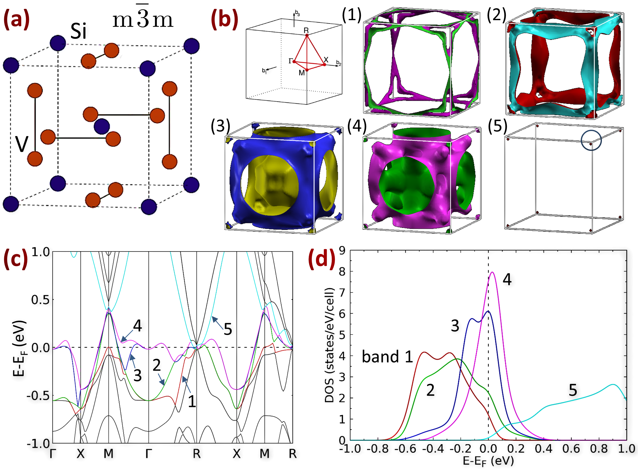
has a primitive cubic crystal structure in space group 223 () with V sitting at 6c and Si at 2a positions as shown in Fig.1(a). The band structure of , Fig.1(c) has flat pieces along -X, -M and -R directions, which is similar to , another A15 superconductor with the same group of elements. There are five bands crossing the as highlighted in different colors in Fig.1(c). The corresponding partial densities of state (DOS) of these bands are plotted in Fig.1(d) and summarized in Table 1. Among them, bands 1 and 2 are hole bands with states gathering along the M-R direction, the edges of the cubic Brillouin zone (BZ) (see Fig.1(b)((1) and (2)). On the other hand, band 5 has a very small electron pocket around the R point, and the contribution to DOS is negligibly small. In contrast, bands 3 and 4 are dominant in DOS at , which corresponds to most of the flat band contributions around the point as seen in Fig.1(c). The three-dimensional (3D) Fermi surfaces (FS) in Fig.1(b)((3) and (4)) show complex FS for both bands 3 and 4, which have multiple sheets at . Analysis of Fig.1(b) suggests that the five bands can be naturally grouped in two effective ones. Specifically, bands 1 and 2 are well separated in energy from bands 3 and 4 at intermediate values inside the BZ, making the inter-band transitions improbable. Furthermore, bands 1 and 2 are much closer in energy, and this is also true for bands 3 and 4, but at different . This suggests grouping bands 1 and 2 into an effective band , bands 3 and 4 into another effective band , and discarding negligible-DOS band 5. Electronic parameters of all five bands are reported in Table.1. The “effective” parameters of two effective bands, and , are given in the last two columns. The multi-band average for band is , and similar for the effective band . As we explain in the two-band model Section III.C, the relative contribution of each band to the superfluid density, is given by the parameter, (hence, model). As shown in Table 1, we estimate , which is quite close to the experimental , discussed in the next Section III.C.
The high DOS at in indicates electronic instability, consistent with literature reports [11, 10, 3]. Although one way to reduce such instability is to promote an exchange splitting, giving a magnetic solution at the DFT level, experimentally is not magnetic. Another way to lift the electronic instability is through the electron-phonon coupling. Similar band structure with flat bands in is susceptible to lattice distortion by a phonon mode [69], indicating a strong electron-phonon coupling in such compounds, hence obvious connection to superconductivity. Thus, the non-magnetic electronic band structure of provides important microscopic details for superconductivity models, such as DOS at and Fermi velocity, which have been used successfully for MgB2, the first proven two-band superconductor. In fact, we calculated the electronic band structure of as a benchmark to compare with with the original model [7, 29] and one of the first DFT calculations of a two-gap system [67], and obtained similar results.
III.2 London penetration depth and superfluid density
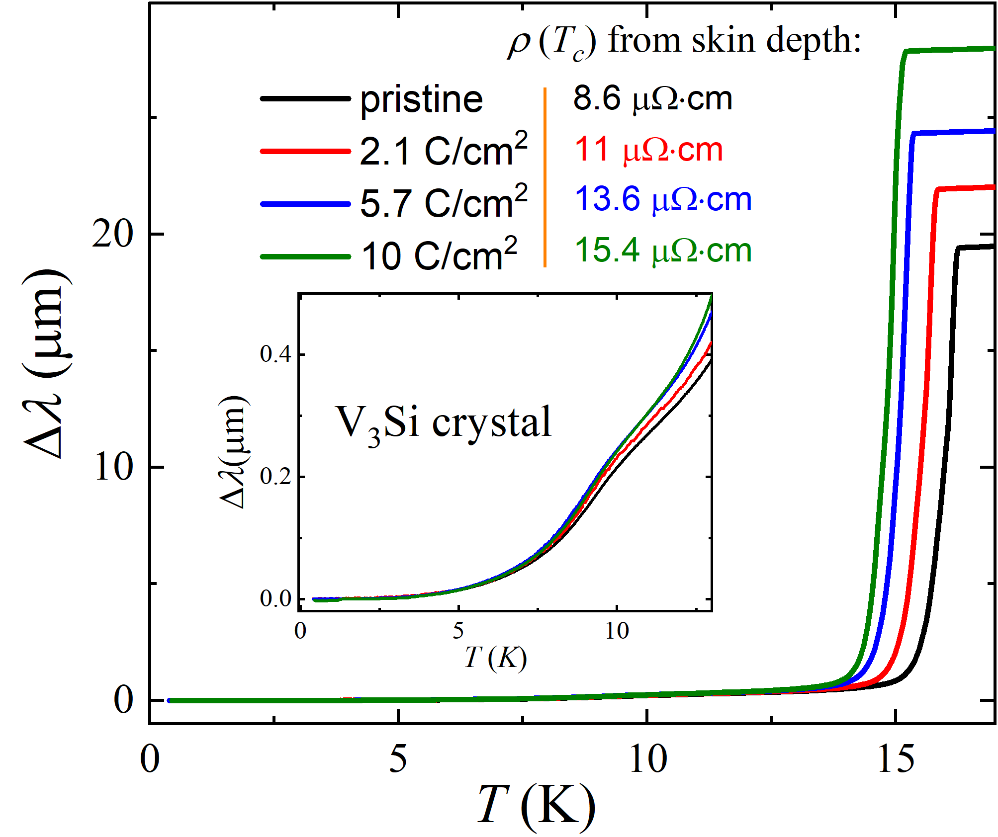
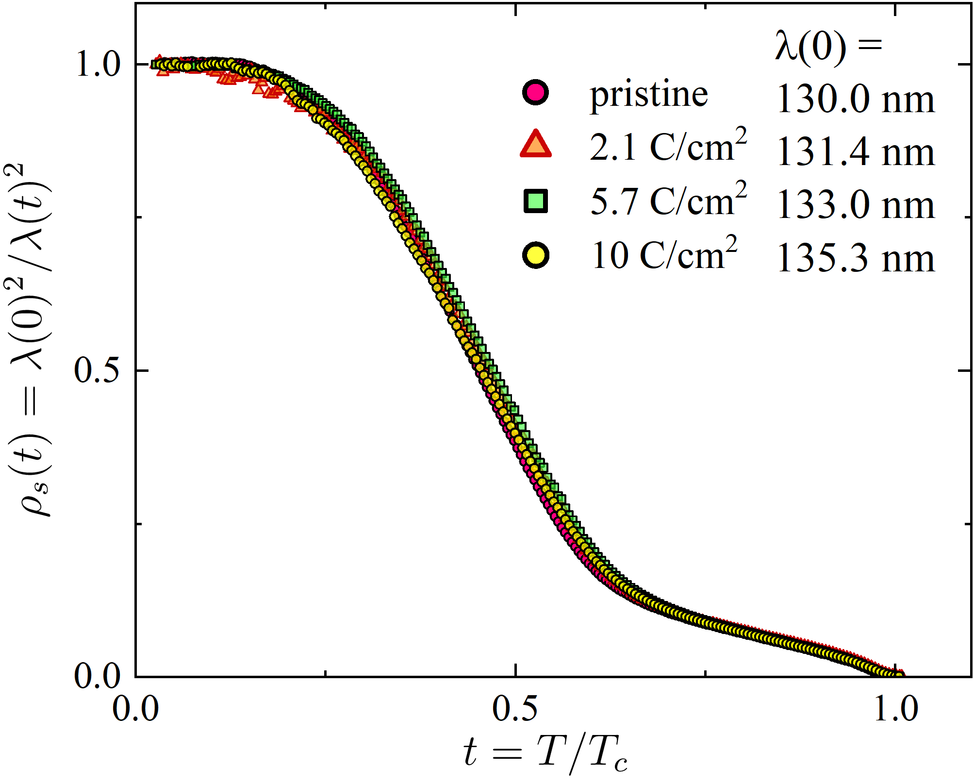
We begin by examining the superfluid density obtained from the measured London penetration depth. Figure 2 shows temperature dependent variation of London penetration depth, , with the increasing dose of electron irradiation. Considering the exponential low-temperature behavior, we can safely assume that and then the normalized superfluid density is calculated as . The inset in Fig.2 zooms at the low-temperature region. There is a clear, almost knee-like feature in around 10 K, which we now know is expected for a two-gap superconductor with different and weakly-coupled gaps [27]. Similar features were reported in high quality crystals before and not surprisingly was interpreted as a definitive evidence of a two-gap superconductivity [7, 30, 7, 30]. The temperature of this kink-like feature is suppressed upon irradiation approximately at the same rate as , signaling that both gaps change at a similar rate. Furthermore, in Fig.2, normal state values above are determined by the skin depth. They increase upon irradiation due to the increase of residual resistivity following the Matthiessen’s rule [70]. Importantly, the superconducting transition temperature, , is monotonically and noticeably suppressed from 16.4 K to 14.7 K (9.3). The upper cut-off at is determined by the normal-metal skin depth, which allows us to estimate the resistivity in a contact-less way using where and , where from Ref.[3, 4]. The extracted resistivity values are 8.6, 11, 13.6, and 15.4 cm for 0, 2.1, 5.7 and 10 C/cm2 electron irradiation doses, respectively. These values appear to be quite comparable with the literature [4, 5, 25]. We note that in a large body of work on , a spread of values ranging from 83 nm to 230 nm can be found. They were obtained using different methods, and in samples of different forms (crystal vs. polycrystalline) and purity [71, 72, 73]. The value we use is within the statistical maximum of the current literature values. Importantly, our results and conclusions are independent of the particular value of .
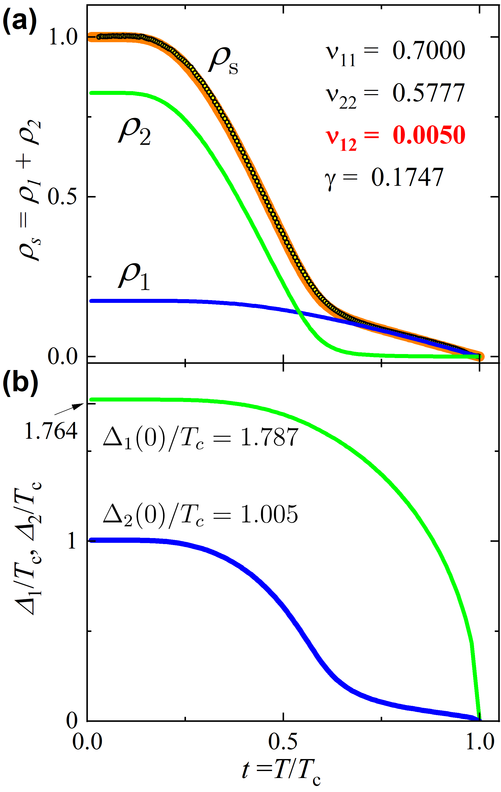
Figure 3 (a) shows the normalized superfluid density of a crystal in pristine state. A similar curve for a different crystal, cut from the same master boule, showing the same two-gap structure, was published in our earlier paper where a self-consistent model based on Eilenberger formalism was introduced [7]. In the original model, two isotropic wave gaps are obtained from the solution of the self-consistency equation, and then all thermodynamic quantities, including the superfluid density, can be calculated. The model was further generalized to include anisotropic or even nodal gaps [74]. Here, it is sufficient to consider the original isotropic approach.
III.3 The isotropic model
The model considers two bands with Fermi velocities, , and the partial densities of states, , where is the total density of states at Fermi level, so that . The dimensionless effective interaction constants are defined as , where is the electron-electron interaction matrix. Note that in the original paper we used for the interaction matrix. To avoid confusion with the London penetration depth, here we use . Also note that this definition differs from that used in the literature, . Our notation has an advantage of being symmetric, . Therefore, for two bands, we have three coefficients of the interaction matrix, two in-band, and , and an inter-band coupling, . In the analysis, we perform a least-squares fit of the experimental superfluid density shown in 3 (a) in Matlab. If all normal-state parameters of a material are known, are the three fitting parameters. They are reduced to two free parameters by the equation for ,
| (1) |
where we assume conventional electron-phonon mechanism of superconductivity with being the Debye frequency. In general, if energy of bosonic pairing “glue” is known, it should be substituted instead of in Eq.1. The pre-factor comes from the weak-coupling approximation used in the model. The effective interaction constant, , is obtained from the solution of algebraic equations containing all coefficients, , see Section II.A of Ref. [7]. To fit the superfluid density, first the self-consistent gap equation is solved at each temperature. Introducing dimensionless quantities, , where , the gaps equations are given by
| (2) |
Note that we often set Boltzmann constant, , where it is obvious, and use it explicitly to emphasize the numerical values or proper dimensions, e.g., Eq.1. For a given set of the coupling constants, , and partial densities of states, , this system can be solved numerically for and therefore provide the energy gaps, . This is a crucial step missing in the so-called model description of the two-band superconductivity [13]. While it was useful early on to explain experimental signatures of two-gap superconductivity in , the fitting parameters of model have little physical meaning. A follow-up study used two-gap functions pre-calculated from the microscopic theory and showed an excellent agreement between experimental and theoretical superfluid density, [75]. Indeed, the wave for which all normal-state parameters are known is a perfect demonstration of the model where different quantities are calculated from obtained from the fit of [7, 29].
Figure 3(b) shows two gaps calculated self-consistently from Eq.2. The individual gap ratios are, and . This should be compared with the results of microwave surface impedance measurements where similar apparent two-gap behavior was observed in the superfluid density and the values of and , quite close to ours, were derived [30]. In the absolute units we obtain, and . After the gaps are calculated, the total superfluid density, can be evaluated and fitted to the experimental data. The partial contributions to the superfluid density are given by [7],
| (3) |
where are the Fermi velocities (not to be confused with Greek of the interaction matrix). Analyzing Fig.1, we group bands 1 and 2 into one effective band , and bands 3 and 4 into another band , and we can safely neglect band 5. (Here we use Roman numerals and to index these “effective” bands). For the first effective band, we find . If we included band 5, it’d make the difference only in 6th decimal digit. Using as another fitting parameter, the best fit of this model to the data gave (fixed by , Eq.1), , , and , with the effective (see Eq.1). Remarkably, the best-fit value of is quite close to the estimate from the electronic band-structure calculations, see Table 1 where we find , . This gives confidence in the model and shows its applicability to describe the superconductivity in . Naturally, overall, smaller partial density of states on band , somewhat counter-intuitively, leads to a larger gap, which is the property of the self-consistent two-band model [7, 35]. We note that the possible uncertainty in the experimental value of leads to some uncertainty in the fitting parameters, but not large enough to alter the general conclusion of the relative amplitudes of the obtained interaction matrix.
III.4 Effect of electron irradiation
In the last three decades, many studies involving particle irradiation were performed on various conventional and unconventional superconductors and there is a vast literature on this topic [76, 77, 78, 42] Due to the differences in the rest mass and irradiation temperature, the number and the morphology of the created defects varies significantly between different projectile particles. It appears that MeV electrons, thanks to a small rest mass, transfer just enough energy upon collision with ions, of the order of tens of eV, to produce well-defined point-like scattering centers [48]. Much larger energy transfer, for example from protons, produce many secondary collisions and less localized damage. A more detailed discussion of electron irradiation and created defects in solids can be found elsewhere [62, 63].
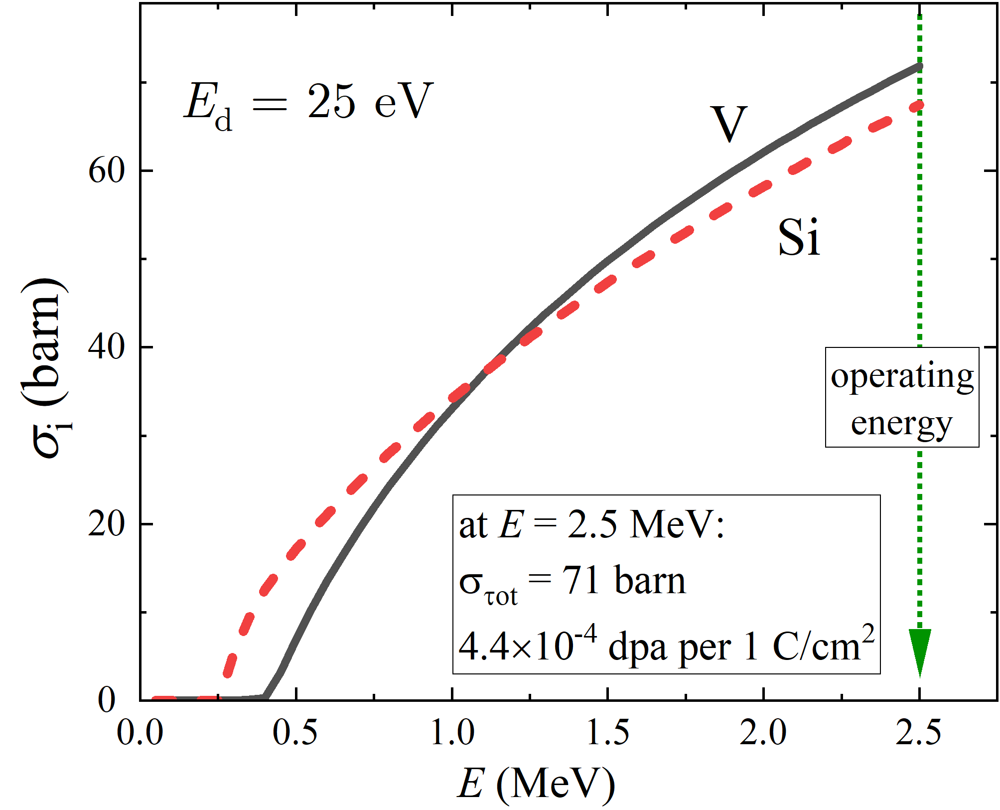
Figure 4 shows the ion-type-resolved cross-sections of the defects creation calculated using SECTE (“Sections Efficaces Calcul Transport d’Électrons”) software, developed at École Polytechnique (Palaiseau, France) by members of the “Laboratoire des Solides Irradiés”, specifically for the interpretation of MeV-range electron irradiation using their Pelletron-type linear accelerator, SIRIUS [79]. Basically, this is a computer-assisted atomic-weights-averaged interpolation of the ion knock-out cross-sections tabulated by O. S. Oen [80]. In the absence of microscopic calculations, we used the commonly assumed value of the ion displacement energy upon a head-on collision, eV. The partial cross-sections are very similar, and we expect a roughly equal number of defects on vanadium and silicon sites. At the operational energy of 2.5 MeV, the total cross-section is estimated as barn, which means that roughly 1.8 defects are produced per 1000 unit formulas per 1 C/cm2. This is a small number of defects that cannot change the electronic structure in any appreciable way, and a significant reduction of observed in our experiments must have a different explanation, such as its pair-breaking nature.
First, let us examine the effect of electron irradiation on superfluid density. While we do not know how much changes, we attempted to adjust its value to scale all curves onto a pristine one. As shown in Fig.5 this worked rather well with a small increase of values shown in the legend. This indicates that scattering does not alter the gap values themselves and, due to very small inter-band coupling, has practically no effect on the total superfluid density. Each isotropic band follows the Anderson theorem [81] and the change in comes mostly from the inter-band scattering between order parameters of different magnitude. We note that the relative change of can be estimated from Tinkham’s widely-used approach [82] that gives for moderate scattering, , where nm is the BCS coherence length, and nm is the electronic mean free path in the pristine state. Both numbers are estimated for V3Si from , Fermi velocity and resistivity, see Table 1 and Fig.2. As shown in Fig.2, at the maximum irradiation dose, the resistivity doubles. Therefore, we expect the increase of by a factor of about 1.3, which is not large and does not alter our conclusions, especially considering an apparent scaling shown in Fig.5 .
III.5 Suppression of by disorder in a two-band superconductor
While it is clear that the superfluid density shows a convincing two-distinct-gaps features implying small inter-band coupling, this still leaves an unanswered important question of the relative sign of the order parameter on each band. This is because superfluid density, as well as any other thermodynamic quantity includes even powers of the gap function, so that an state cannot be distinguished from an state if the gaps are the same, see, for example, Eq.3. The suppression of on the other hand is very sensitive to the overall anisotropy of the order parameter, including a generalized view when two bands are considered side by side along the common path on the entire Fermi surface [83]. This situation can be analyzed employing a very useful ansatz that temperature and angular parts of the order parameter can be separated, , where is Fermi wave vector and the angular part obeys the normalization condition for the Fermi surface average, [83, 84]. For example, for a single band wave, and for a wave, . For a two-gap superconductor Kogan introduced two gaps each described by its own angular part [83]. In this case, the normalization reads,
| (4) |
In the case of an anisotropic gap, even non-magnetic (no spin-flip) scatterers suppress superconducting transition temperature, . With spin-flip scattering both channels reduce . Openov gives a generalized Abrikosov-Gor’kov [85] type expression where gap anisotropy is explicitly taken into account [86, 87]. We note that a more general theory of the suppression by disorder scattering, extended to topologically non-trivial superconductors, is discussed elsewhere [44, 43]. Here it suffice to consider the approach, which gives,
| (5) |
where with being the transition temperature in a pristine state, and is the digamma function. Dimensionless magnetic and non-magnetic scattering rates are given by
| (6) |
where and are non-magnetic and magnetic (spin flip) scattering times, respectively. (Note that original Abrikosov-Gor’kov theory uses a different definition of the scattering rate, , with the actual (suppressed) ). The effect of gap anisotropy can be immediately seen from Eq.5 - it contains in the first power. For a single-band wave, and we obtain recovering the Anderson theorem [81]. For a wave, and we obtain an expression where both magnetic and non-magnetic impurities suppress . It is interesting to note that the critical value for the complete suppression of an wave order parameter by magnetic impurities, , is exactly half of the value for a wave order parameter suppression by non-magnetic impurities, .
We can now use Eq.5 with the two-gaps approach, Eq.4 and that . Specifically, we consider two isotropic gaps described by constant values and . In other words, two bands are represented in a generalized single angular coordinate, - band 1 from to , and band 2 from to , each with its own density of states , so that the partial densities of states are . Introducing the gap ratio, and the ratio of the partial densities of state, =N, we obtain for the total average in this two-gap model:
| (7) |
Without magnetic scattering (), the transition temperature of a two-band superconductor is,
| (8) |
It is important to emphasize that the superfluid density as a function of (reduced) temperature and are two independent measurements, which makes the analysis better defined and constrained.
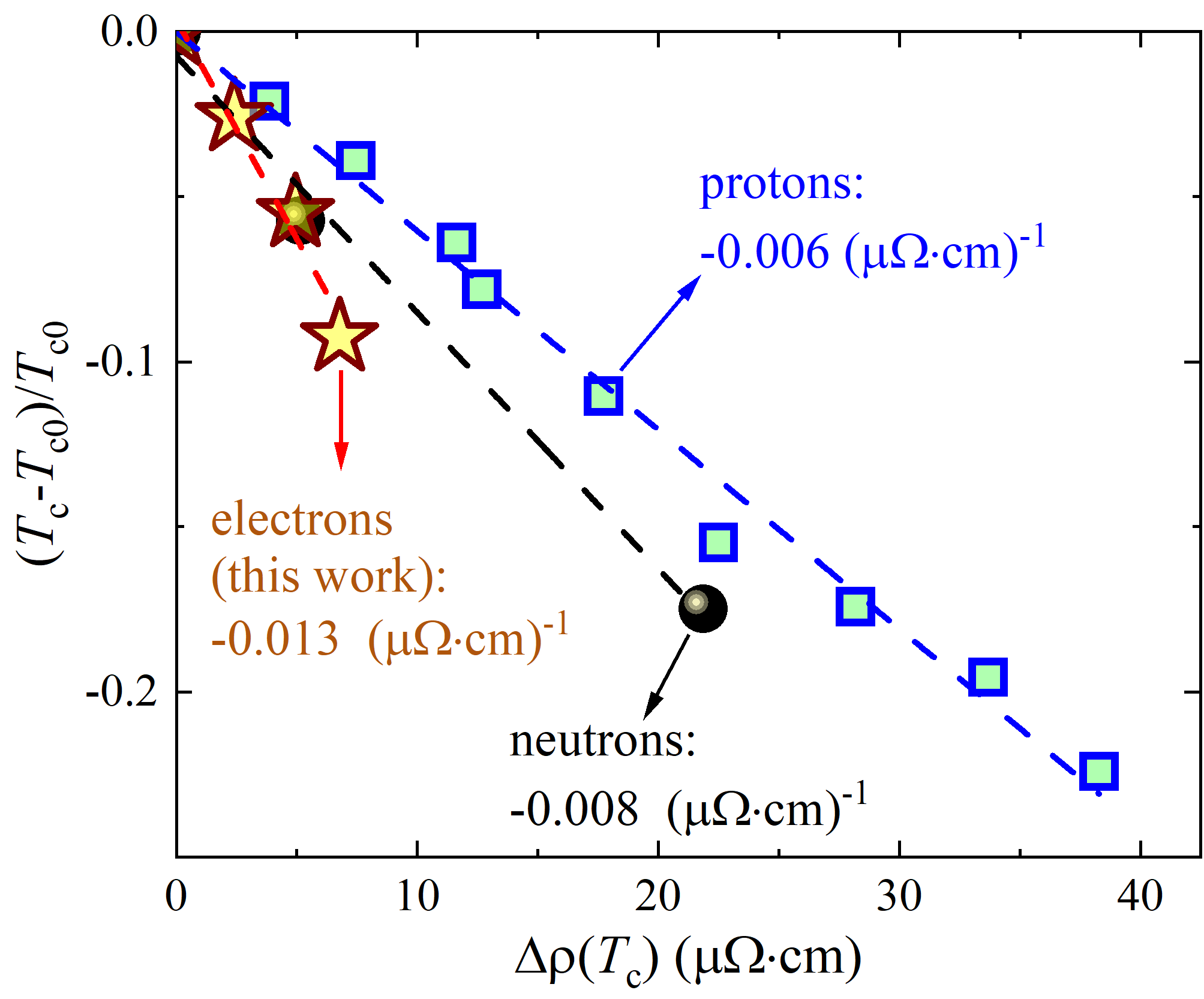
To compare the experimentally observed decrease of with our model, we need a proper parameter characterizing the scattering rate. The problem is that different sources of disorder produce somewhat different effects. Figure 6 compares the relative change of the transition temperature, , in per of resistivity increase caused by electron irradiation in the current study with two previous studies where defects were induced by proton [88] and neutron [5] irradiation. The rates of the relative change are, (electron irradiation), -0.008 (neutron), and -0.006 (proton). Due to their small rest mass and matching range of the energy transfer (1-100 eV), electrons produce the most efficient point-like defects and have the largest suppression rate. A similar trend is observed in other materials, for example, well-studied iron-based superconductors [42, 48]. On the other hand, the observed rates are not too different, roughly 0.01 , and we can put it in a perspective by comparing with other superconductors. For that, we need to calculate the dimensionless scattering rate, Eq.6. In our case of measured and the simplest estimate of the scattering time, , is via the London and Drude electrodynamics, . Note that clean-limit value, , needed for the density of states in the normal metal, enters this estimate, whereas (normal metal) scattering time comes from resistivity. This approach is well justified in isotropic wave superconductors and compounds assuming that the gap smearing caused by the modest amounts of non-magnetic disorder is much smaller than the gap amplitudes.
In our case, we can use Tinkham’s widely-used approach [82] that gives for moderate scattering, , where nm is the BCS coherence length, and nm is the electronic mean free path in the pristine state. Both numbers are estimated for V3Si from , Fermi velocity and resistivity, see Table 1 and Fig.2. As shown in Fig.2, at the maximum irradiation dose, the resistivity doubles. Therefore, we expect the increase of by a factor of about 1.3. This is an insignificant change to alter the main features reported here - the exponential attenuation at low temperatures and a higher temperature kink signaling of two barely-coupled gaps of different magnitude. This is further confirmed by the apparent scaling of the superfluid density for all doses of electron irradiation, Fig.5.
The experimental dimensionless scattering rate can be estimated as,
| (9) |
Note that we measure resistivity change with respect to the pristine sample to subtract inelastic scattering, but this also removes background impurity scattering in samples before irradiation. Fortunately, judging by very low pinning, this correction is negligible [26]. Also, note that this dimensionless rate contains unmodified , which is different from the original Abrikosov-Gor’kov definition [85].
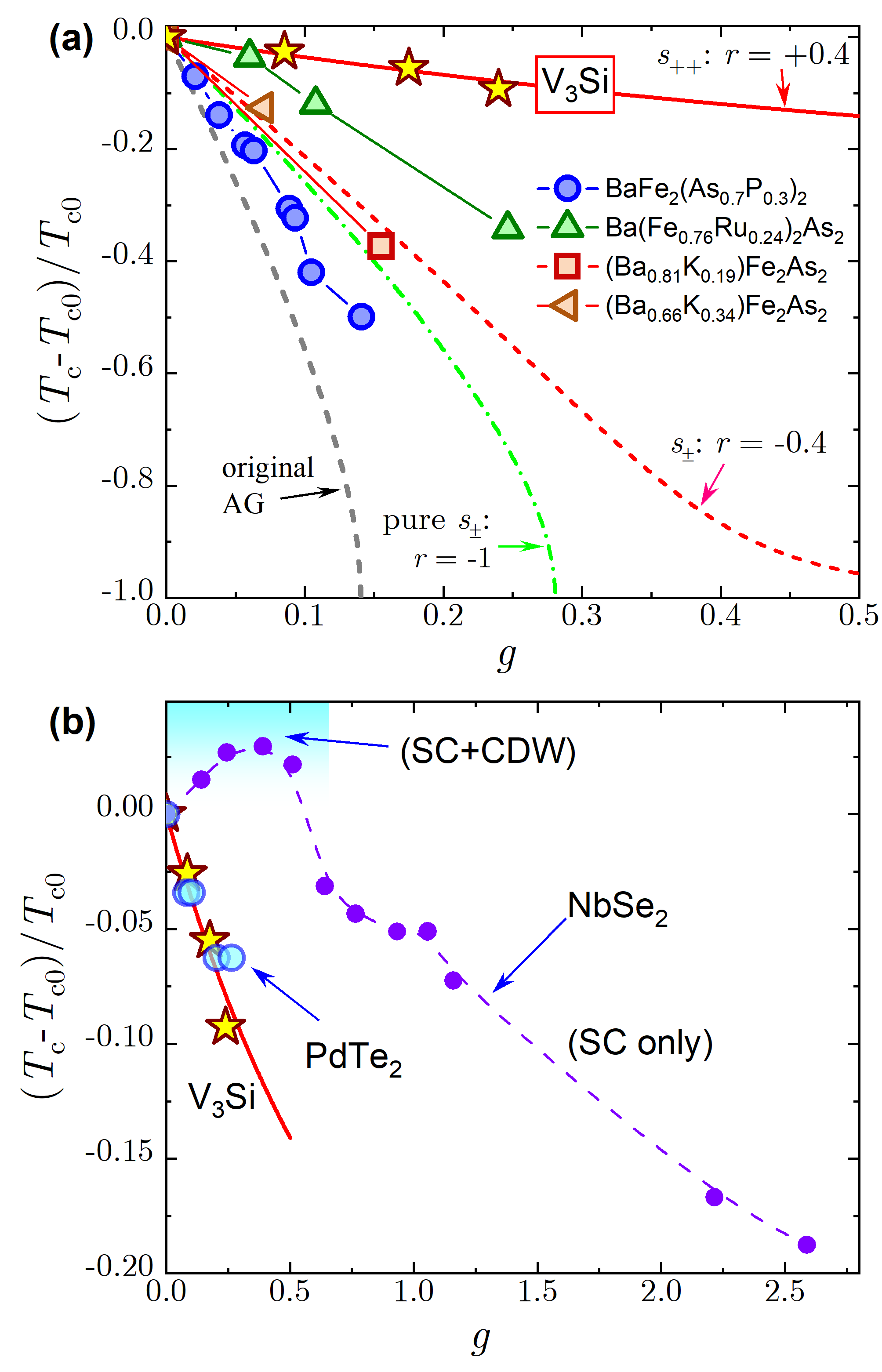
Figure 7 shows the normalized change of superconducting transition temperature, , as function of the dimensionless scattering rate, . Figure 7(a) compares single crystal with known nodeless and nodal superconductors, isovalently substituted and , and hole- doped underdoped and optimally-doped (BaK122) [42]. The theoretical curves from Eq.8 are shown by different lines. Clearly, all sign-changing superconductors show suppression rate significantly higher than in two-gap , which is consistent with theoretical curve for gap ratio, , while the same gap ratio, but of opposite signs, , is close to BaK122 data. Interestingly, a nodal multi-band superconductor, , shows even greater rate of suppression, most likely because in this case the inter-band and in-band scattering channels are both pair-breaking. Figure 7(b) compares with another two-band superconductor, [89], and unconventional Dirac semi-metal compound, [43, 90]. In , the situation is complicated by the charge-density wave (CDW), whose competition with superconductivity (SC) leads to the initial increase of . However, as soon as CDW is destroyed by disorder, further suppression of is quite similar to our subject compound, [89]. The second compound, unconventional shows the rate of suppression quite similar to . Moreover, it also has a fully-gapped Fermi surface leading to exponential attenuation of the penetration depth. However, peculiarities of the electronic band structure of support unconventional pairing mechanism [43, 90], whereas does not have such topological features and is consistent with BCS-type two-gap superconductivity. This is a good example showing that measurements alone cannot answer objectively. They must be supported by theoretical analysis.
IV Conclusions
We used controlled point-like disorder induced by 2.5 MeV electron irradiation at different doses to study superconducting order parameter in a single crystal. Simultaneous measurements of London penetration depth and superconducting transition temperature, , set stringent experimental boundaries on possible superconducting states. Specifically, we observe: (1) exponentially attenuated low-temperature behavior of (which means a fully gapped Fermi surface); (2) a kink at higher reduced temperatures (signaling of two barely-coupled gaps); (3) a significant shift of (gaps of different amplitude). The discussed analysis is applicable for any choice of . Using a two-band analysis for both quantities, and , we conclude that pairing with two barely-coupled gaps of different amplitudes, and , provide an excellent fit and overall self-consistent description of the experiment. This makes the earliest (superconductivity discovered in 1953) proven superconductor, preceding (superconductivity discovered in 2001) by half a century.
Acknowledgements.
We thank David Christen for providing excellent single crystals well-characterized in his earlier papers. This work was supported by the US Department of Energy (DOE), Office of Science, Basic Energy Sciences, Materials Science and Engineering Division. Ames Laboratory is operated for the US DOE by Iowa State University under contract DE-AC02-07CH11358. The authors acknowledge support from the EMIR&A French network (FR CNRS 3618) on the “SIRIUS” platform under proposal # 18-5155. We thank the whole SIRIUS team, O. Cavani, B. Boizot, V. Metayer, and J. Losco, for operating electron irradiation facility.References
- Hardy and Hulm [1953] G. F. Hardy and J. K. Hulm, Phys. Rev. 89, 884 (1953).
- Blezius and Carbotte [1986] J. W. Blezius and J. P. Carbotte, Phys Rev B 33, 3509 (1986).
- Wu et al. [1994] W. D. Wu, A. Keren, L. P. Le, G. M. Luke, B. J. Sternlieb, Y. J. Uemura, D. C. Johnston, B. K. Cho, and P. Gehring, Hyperfine Interact. 86, 615 (1994).
- Testardi et al. [1977] L. R. Testardi, J. M. Poate, and H. J. Levinstein, Phys. Rev. B 15, 2570 (1977).
- Viswanathan and Caton [1978] R. Viswanathan and R. Caton, Phys. Rev. B 18, 15 (1978).
- Khlopkin [1999] M. N. Khlopkin, Journal of Experimental and Theoretical Physics Letters 69, 26 (1999).
- Kogan et al. [2009] V. G. Kogan, C. Martin, and R. Prozorov, Phys. Rev. B 80, 014507 (2009).
- Tanaka et al. [2010] S. Tanaka, A. Miyake, T. Kagayama, K. Shimizu, B. Salce, and D. Braithwaite, J. Phys. Conf. Ser. (Online) 200, 3 (2010).
- Goldberg and Weger [1972] I. B. Goldberg and M. Weger, Le Journal de Physique Colloques 33, C3 (1972).
- Klein et al. [1978] B. M. Klein, L. L. Boyer, D. A. Papaconstantopoulos, and L. F. Mattheiss, Phys. Rev. B 18, 6411 (1978).
- Bok and Bouvier [2012] J. Bok and J. Bouvier, J. Supercond. Novel Magn. 25, 657 (2012).
- Nagamatsu et al. [2001] J. Nagamatsu, N. Nakagawa, T. Muranaka, Y. Zenitani, and J. Akimitsu, Nature 410, 63 (2001).
- Bouquet et al. [2001] F. Bouquet, Y. Wang, R. A. Fisher, D. G. Hinks, J. D. Jorgensen, A. Junod, and N. E. Phillips, Europhys. Lett. 56, 856 (2001).
- Kortus et al. [2001] J. Kortus, I. I. Mazin, K. D. Belashchenko, V. P. Antropov, and L. L. Boyer, Phys. Rev. Lett. 86, 4656 (2001).
- Bud’ko et al. [2001] S. L. Bud’ko, G. Lapertot, C. Petrovic, C. E. Cunningham, N. Anderson, and P. C. Canfield, Phys. Rev. Lett. 86, 1877 (2001).
- Bardeen et al. [1957] J. Bardeen, L. N. Cooper, and J. R. Schrieffer, Phys. Rev. 106, 162 (1957).
- Moskalenko [1959] V. A. Moskalenko, Fiz. Met. Metalloved. (USSR); [Phys. Met. Metallogr. 8, 25 (1959)] 8:4 (1959).
- Suhl et al. [1959] H. Suhl, B. T. Matthias, and L. R. Walker, Phys. Rev. Lett. 3, 552 (1959).
- Geilikman et al. [1967] B. T. Geilikman, R. O. Zaitsev, and V. Z. Kresin, Sov. Phys.- Solid State (Engl. Transl.), 9: 642-7(Sept. 1967). (1967).
- Mazin et al. [1993] I. Mazin, A. Liechtenstein, C. Rodriguez, O. Jepsen, and O. Andersen, Physica C: Superconductivity 209, 125 (1993).
- Golubov et al. [1994] A. Golubov, O. Dolgov, E. Maksimov, I. Mazin, and S. Shulga, Physica C: Superconductivity 235-240, 2383 (1994).
- Golubov and Mazin [1995] A. Golubov and I. Mazin, Physica C: Superconductivity 243, 153 (1995).
- Golubov and Mazin [1997] A. A. Golubov and I. I. Mazin, Phys. Rev. B 55, 15146 (1997).
- Viswanathan et al. [1978] R. Viswanathan, R. Caton, and C. S. Pande, Phys. Rev. Lett. 41, 906 (1978).
- Orlando et al. [1979] T. P. Orlando, E. J. McNiff, S. Foner, and M. R. Beasley, Phys. Rev. B 19, 4545 (1979).
- Kogan et al. [1997] V. G. Kogan, P. Miranović, L. Dobrosavljević-Grujić, W. E. Pickett, and D. K. Christen, Phys. Rev. Lett. 79, 741 (1997).
- Prozorov and Kogan [2011] R. Prozorov and V. G. Kogan, Rep. Prog. Phys. 74, 124505 (2011).
- Zehetmayer and Hecher [2014] M. Zehetmayer and J. Hecher, Supercon. Sci. Tech. 27, 044006 (2014).
- Kim et al. [2019] H. Kim, K. Cho, M. A. Tanatar, V. Taufour, S. K. Kim, S. L. Bud’ko, P. C. Canfield, V. G. Kogan, and R. Prozorov, Symmetry 11, 1012 (2019).
- Nefyodov, Yu. A. et al. [2005] Nefyodov, Yu. A., Shuvaev, A. M., and Trunin, M. R., Europhys. Lett. 72, 638 (2005).
- Perucchi et al. [2010] A. Perucchi, D. Nicoletti, M. Ortolani, C. Marini, R. Sopracase, S. Lupi, U. Schade, M. Putti, I. Pallecchi, C. Tarantini, M. Ferretti, C. Ferdeghini, M. Monni, F. Bernardini, S. Massidda, and P. Dore, Phys. Rev. B 81, 092509 (2010).
- Tanaka et al. [2012] S. Tanaka, Handoko, A. Miyake, T. Kagayama, K. Shimizu, A. Bohmer, P. Burger, F. Hardy, C. Meingast, T. Tsutsami, and Y. Onuki, J. Phys. Soc. Jpn. 81, SB026 (2012).
- Testardi and Bateman [1967] L. R. Testardi and T. B. Bateman, Phys. Rev. 154, 402 (1967).
- Carrington [2011] A. Carrington, C. R. Phys. 12, 502 (2011).
- Kogan and Prozorov [2016] V. G. Kogan and R. Prozorov, Phys. Rev. B 93, 224515 (2016).
- van Harlingen [1995] D. J. van Harlingen, Rev. Mod. Phys. 67, 515 (1995).
- Golubov and Mazin [2013] A. A. Golubov and I. I. Mazin, Appl. Phys. Lett. 102, 032601 (2013).
- Sykora and Coleman [2011] S. Sykora and P. Coleman, Phys. Rev. B 84, 054501 (2011).
- Hanaguri et al. [2010] T. Hanaguri, S. Niitaka, K. Kuroki, and H. Takagi, Science 328, 474 (2010).
- Efremov et al. [2011] D. V. Efremov, M. M. Korshunov, O. V. Dolgov, A. A. Golubov, and P. J. Hirschfeld, Phys. Rev. B 84, 180512 (2011).
- Ghigo et al. [2018] G. Ghigo, D. Torsello, G. A. Ummarino, L. Gozzelino, M. A. Tanatar, R. Prozorov, and P. C. Canfield, Phys. Rev. Lett. 121, 107001 (2018).
- Cho et al. [2018a] K. Cho, M. Kończykowski, S. Teknowijoyo, M. A. Tanatar, and R. Prozorov, Supercon. Sci. Tech. 31, 064002 (2018a).
- Teknowijoyo et al. [2018] S. Teknowijoyo, N. H. Jo, M. S. Scheurer, M. A. Tanatar, K. Cho, S. L. Bud'ko, P. P. Orth, P. C. Canfield, and R. Prozorov, Phys. Rev. B 98, 024508 (2018).
- Krenkel [2021] E. H. Krenkel, arxiv:AAA.BBB (2021).
- Gross et al. [1986] F. Gross, B. S. Chandrasekhar, D. Einzel, K. Andres, P. J. Hirschfeld, H. R. Ott, J. Beuers, Z. Fisk, and J. L. Smith, Zeitschrift für Physik B Condensed Matter 64, 175 (1986).
- Gross-Alltag et al. [1991] F. Gross-Alltag, B. S. Chandrasekhar, D. Einzel, P. J. Hirschfeld, and K. Andres, Zeitschrift für Physik B Condensed Matter 82, 243 (1991).
- Mizukami et al. [2014] Y. Mizukami, M. Konczykowski, Y. Kawamoto, S. Kurata, S. Kasahara, K. Hashimoto, V. Mishra, A. Kreisel, Y. Wang, P. J. Hirschfeld, Y. Matsuda, and T. Shibauchi, Nat Commun 5, 10.1038/ncomms6657 (2014).
- Ghimire et al. [2021] S. Ghimire, M. Kończykowski, K. Cho, M. A. Tanatar, D. Torsello, I. S. Veshchunov, T. Tamegai, G. Ghigo, and R. Prozorov, Materials 14, 3267 (2021).
- Takenaka et al. [2017] T. Takenaka, Y. Mizukami, J. Wilcox, M. Konczykowski, S. Seiro, C. Geibel, Y. Tokiwa, Y. Kasahara, C. Putzke, Y. Matsuda, A. Carrington, and T. Shibauchi, Phys. Rev. Lett. 119, 077001 (2017).
- Cho et al. [2016] K. Cho, M. Kończykowski, S. Teknowijoyo, M. A. Tanatar, Y. Liu, T. A. Lograsso, W. E. Straszheim, V. Mishra, S. Maiti, P. J. Hirschfeld, and R. Prozorov, Sci. Adv. 2, e1600807 (2016).
- Putti et al. [2006] M. Putti, M. Affronte, C. Ferdeghini, P. Manfrinetti, C. Tarantini, and E. Lehmann, Phys. Rev. Lett. 96, 077003 (2006).
- Schilling et al. [2016] M. B. Schilling, A. Baumgartner, B. Gorshunov, E. S. Zhukova, V. A. Dravin, K. V. Mitsen, D. V. Efremov, O. V. Dolgov, K. Iida, M. Dressel, and S. Zapf, Phys. Rev. B 93, 174515 (2016).
- Kim et al. [2012] J. Kim, N. Haberkorn, M. J. Graf, I. Usov, F. Ronning, L. Civale, E. Nazaretski, G. F. Chen, W. Yu, J. D. Thompson, and R. Movshovich, Phys. Rev. B 86, 144509 (2012).
- Yethiraj et al. [1999] M. Yethiraj, D. K. Christen, D. M. Paul, P. Miranovic, and J. R. Thompson, Phys. Rev. Lett. 82, 5112 (1999).
- Yethiraj et al. [2005] M. Yethiraj, D. K. Christen, A. A. Gapud, D. M. Paul, S. J. Crowe, C. D. Dewhurst, R. Cubitt, L. Porcar, and A. Gurevich, Phys. Rev. B 72, 10.1103/PhysRevB.72.060504 (2005).
- Prozorov and Giannetta [2006] R. Prozorov and R. W. Giannetta, Supercon. Sci. Tech. 19, R41 (2006).
- Van Degrift [1975] C. T. Van Degrift, Rev. Sci. Instrum. 46, 599 (1975).
- Prozorov et al. [2000a] R. Prozorov, R. W. Giannetta, A. Carrington, and F. M. Araujo-Moreira, Phys. Rev. B 62, 115 (2000a).
- Prozorov et al. [2000b] R. Prozorov, R. W. Giannetta, A. Carrington, P. Fournier, R. L. Greene, P. Guptasarma, D. G. Hinks, and A. R. Banks, Appl. Phys. Lett. 77, 4202 (2000b).
- Prozorov [2021] R. Prozorov, Phys. Rev. Applied 16, 024014 (2021).
- Prozorov et al. [2014] R. Prozorov, M. Kończykowski, M. A. Tanatar, A. Thaler, S. L. Bud’ko, P. C. Canfield, V. Mishra, and P. J. Hirschfeld, Phys. Rev. X 4, 041032 (2014).
- Damask and Dienes [1963] A. C. Damask and G. J. Dienes, Point Defects in Metals (Gordon & Breach Science Publishers Ltd, 1963).
- Thompson [1969] M. W. Thompson, Defects and Radiation Damage in Metals, September 27, 1974 ed., Cambridge Monographs on Physics (Cambridge University Press, 1969).
- Perdew et al. [1996] J. P. Perdew, K. Burke, and M. Ernzerhof, Phys. Rev. Lett. 77, 3865 (1996).
- Tanaka et al. [2011] S. Tanaka, A. Miyake, T. Kagayama, and K. Shimizu, J. Phys.: Conf. Ser. 273, 012105 (2011).
- Kresse and Furthmüller [1996] G. Kresse and J. Furthmüller, Phys. Rev. B 54, 11169 (1996).
- Belashchenko et al. [2001] K. D. Belashchenko, M. van Schilfgaarde, and V. P. Antropov, Phys. Rev. B 64, 092503 (2001).
- Torsello et al. [2020] D. Torsello, G. Ummarino, J. Bekaert, L. Gozzelino, R. Gerbaldo, M. Tanatar, P. Canfield, R. Prozorov, and G. Ghigo, Phys. Rev. Applied 13, 064046 (2020).
- Sadigh and Ozoliņš [1998] B. Sadigh and V. Ozoliņš, Phys. Rev. B 57, 2793 (1998).
- Matthiessen and Vogt [1864] A. Matthiessen and C. Vogt, Philos. Trans. R. Soc. Lond. 154, 167 (1864).
- Hanaguri et al. [1995] T. Hanaguri, Y. Iino, A. Maeda, and T. Fukase, Phys. C Supercond. its Appl. 246, 223 (1995).
- Greytak and Wernick [1964] T. J. Greytak and J. H. Wernick, J. Phys. Chem. Solids 25, 535 (1964).
- Muto et al. [1979] Y. Muto, N. Toyota, K. Noto, K. Akutsu, M. Isino, and T. Fukase, J. Low Temp. Phys. 34, 617 (1979).
- Li et al. [2016] M. Li, N. R. Lee-Hone, S. Chi, R. Liang, W. N. Hardy, D. A. Bonn, E. Girt, and D. M. Broun, New J. Phys. 18, 082001 (2016).
- Fletcher et al. [2005] J. D. Fletcher, A. Carrington, O. J. Taylor, S. M. Kazakov, and J. Karpinski, Phys. Rev. Lett. 95, 097005 (2005).
- Brown and Cost [1990] R. D. Brown and J. R. Cost, JOM 42, 39 (1990).
- Weber [1986] H. W. Weber, in Advances in Cryogenic Engineering Materials (Springer US, 1986) pp. 853–864.
- Tamegai et al. [2012] T. Tamegai, T. Taen, H. Yagyuda, Y. Tsuchiya, S. Mohan, T. Taniguchi, Y. Nakajima, S. Okayasu, M. Sasase, H. Kitamura, T. Murakami, T. Kambara, and Y. Kanai, Supercon. Sci. Tech. 25, 084008 (2012).
- [79] The SIRIUS linear accelerator: https://portail.polytechnique.edu/lsi/en/facilities/sirius-installation.
- Oen [1973] O. S. Oen, Cross sections for atomic displacements in solids by fast electrons, Tech. Rep. (Office of Scientific and Technical Information (OSTI), ID: 4457758, Report Num.: ORNL-4897, 1973).
- Anderson [1959] P. Anderson, J. Phys. Chem. Solids 11, 26 (1959).
- Tinkham [2004] M. Tinkham, Introduction to Superconductivity, 2nd ed., Dover Books on Physics (Dover Publications, 2004).
- Kogan [2002] V. G. Kogan, Phys. Rev. B 66, 020509 (2002).
- Kogan et al. [2019] V. G. Kogan, R. Prozorov, and A. E. Koshelev, Phys. Rev. B 100, 014518 (2019).
- Abrikosov and Gor’kov [1960] A. A. Abrikosov and L. P. Gor’kov, Zh. Eksp. Teor. Fiz. (Sov. Phys. JETP 12, 1243 (1961)) 39, 1781 (1960).
- Openov [1997] L. A. Openov, Journal of Experimental and Theoretical Physics Letters 66, 661 (1997).
- Openov [2004] L. A. Openov, Phys. Rev. B 69, 224516 (2004).
- Alterovitz et al. [1981] S. A. Alterovitz, D. E. Farrell, B. S. Chandrasekhar, E. J. Haugland, J. W. Blue, and D. C. Liu, Phys. Rev. B 24, 90 (1981).
- Cho et al. [2018b] K. Cho, M. Kończykowski, S. Teknowijoyo, M. A. Tanatar, J. Guss, P. B. Gartin, J. M. Wilde, A. Kreyssig, R. J. McQueeney, A. I. Goldman, V. Mishra, P. J. Hirschfeld, and R. Prozorov, Nat Commun 9, 2796 (2018b).
- Timmons et al. [2020] E. I. Timmons, S. Teknowijoyo, M. Kończykowski, O. Cavani, M. A. Tanatar, S. Ghimire, K. Cho, Y. Lee, L. Ke, N. H. Jo, S. L. Bud'ko, P. C. Canfield, P. P. Orth, M. S. Scheurer, and R. Prozorov, Phys. Rev. Research 2, 023140 (2020).