At the verge of topology: vacancy-driven quantum spin Hall in trivial insulators
Abstract
Vacancies in materials structure – lowering its atomic density – take the system closer to the atomic limit, to which all systems are topologically trivial. Here we show a mechanism of mediated interaction between vacancies inducing a topologically non-trivial phase. Within an ab initio approach we explore topological transition dependence with the vacancy density in transition metal dichalcogenides. As a case of study, we focus on the PtSe2, to which pristine form is a trivial semiconductor with an energy gap of eV. The vacancies states lead to a large topological gap of meV within the pristine system gap. We derive an effective model describing this topological phase in other transition metal dichalcogenide systems. The mechanism driving the topological phase allows the construction of backscattering protected metallic channels embedded in a semiconducting host.
keywords:
Transition metal dichalcogenides, topological insulator, vacancy, phase transition![[Uncaptioned image]](/html/2109.11915/assets/x1.png)
The introduction of defects in materials has allowed extensive experimental modification of their properties. The most basic defect unit in materials is atoms vacancies. These localized defects in contrast with the more complex dislocations and grain boundaries can be directly induced and controlled experimentally 1, 2. Vacancies centers can act as active catalytic sites 3, but also drive exotic effects, for instance, as charge density waves in In nanowires on Si(111) 4 and ferromagnetism on transition metal dichalcogenides (TMD) 5. Electronic phase transition (metal-insulator) have also taken place mediated by vacancy formations in GeSbTe 6.
A recent class of system presenting quantum topological transition have gained the interest in recent year. These systems present insulating behavior in their bulk but metallic surface states with symmetry stabilized backscattering protection. The defect-induced topological transition was observed in alloy systems by replacing atoms keeping within the same atomic density. For instance, in (Bi1-xInx)2Se3 a topological non-trivial to trivial insulating phase is achieved with an increase in the alloying parameter 7, that is, increasing the defect concentration lead to the topological phase to vanishes. Additionally, keeping the same atomic density, Anderson random disorder have also shown to drive a topological transition on HgTe quantum wells 8, 9. Besides substitutional defects, vacancy formation, i.e. reducing the atomic density, takes the systems towards the atomic limit to which all systems are trivial.
In this paper, we show that another phenomena can take place, where the vacancy states give rise to a topological phase, that is, a trivial to non-trivial topological transition with the increase in defects concentration. Taking an ab initio approach based on the density functional theory (DFT) we investigate the vacancy driven topology in the trivial semiconductor PtSe2. Extrapolating to general TMD systems, a simple model was derived to describe the threshold vacancy density for the topology to emerge. The vacancy states within the host bandgap allow topological states to be constructed within a semiconducting matrix.
Se vacancy on PtSe2 is the most energetically favorable defect 10. Experimental Se vacancy formation on PtSe2 can be controlled by electron irradiation 11, while its assembly can be achieved by a thermal treatment 12 by the mobility of such defects 13. Additionally, with the recent advances on controlled atomic positioning on surfaces by AFM/STM tips 14, 15, 16, controlled Se vacancies have been induced on the TMD PdSe2 17.
From the electronic perspective, an isolated Se vacancy introduces localized states in the host PtSe2 bandgap. Upon the removal of a Se atom, three lone pairs arise in the Pt atoms neighboring the vacancy. By increasing the vacancy density, those states can interact with each other forming energy bands. Indeed the in-gap vacancy states, have a major contribution from Pt /, with its interaction mediated by the host Se orbitals 10. Such a picture of interacting vacancy states within the host energy gap, ruling a hopping mediated charge transport, is experimentally observed in TMD 18. The dispersion of those in-gap vacancy states (ruled by the vacancy concentration), allied with the host TMD spin-orbit coupling (SOC) has the ingredients for a possible topologically non-trivial phase. In Figure 1(a) we show a single vacancy on a PtSe2 33 supercell, taking different supercell sizes defines the Se vacancy concentration on this system. In Figure 1(b) we shown the DFT calculated band structure, with the red bands being the vacancy states neatly laying within the host gap states (blue bands). We see that the in-gap states (red bands) are dispersive for higher vacancy densities [Figure 1(b)] (smaller supercell size), with its dispersion getting narrower with decreasing vacancy density. It is worth pointing out that the discussed Se-vacancy densities are within the values achieved experimentally in PtSe2, up to vac/cm2 (PtSe1.75) 12, with observed chalcogenides monovacancies in other TMD reaching up to vac/cm2 (MoS1.54) 19.
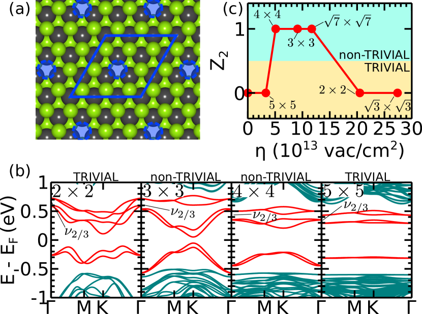
The spin-orbit coupling effect within the vacancy states can lead to topological phases. Indeed we have calculated the invariant for the two energy gaps of the vacancy states, at filing (at the Fermi energy), and filing (above the Fermi energy). At filing all systems are trivial, however at we found a topological transition with the vacancy density increase [Figure 1(c)]. The system with zero vacancies (), pristine PtSe2, is a trivial semiconductor with a eV bandgap. Introducing low vacancy densities, vac/cm2, the system is still trivial as the vacancies states are localized and do not interact with each other. Increasing the vacancy density such scenario change and the interaction between the vacancy states leads to a topological phase up to vac/cm2 (PtSe1.94). The electron doping required to access the filing topological gap is which is accessible in 2D systems by gating interfaces 20. Further increasing of the vacancy density leads to a re-entrant trivial phase. It is worth pointing out that we have introduced the vacancies in other crystalline cell geometries, for instance in a tetragonal cell, and the same behavior is observed concerning the topological phase and vacancy concentration. Additionally, 2D topology was recently characterized as robust against disordered assemblies 21, 22.
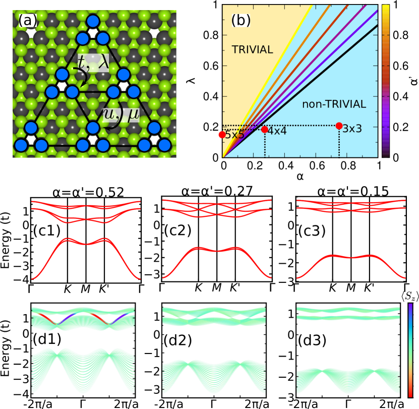
To understand the interplay between the vacancy concentration and the emergence of the non-trivial state, we have extracted a model for the phase transition in the hexagonal geometry. The hamiltonian for the three lone pairs interacting in the presence of SOC is written as
| (1) |
where and describe the hopping between the nearest and next-nearest neighbors sites while and the SOC induced term [as shown in Figure 2(a)]; are the spin Pauli matrix, with the 22 identity matrix, and the sign of the SOC contribution 23. Such Hamiltonian assumes the form
| (2) |
with
| (3) | |||||
| (4) | |||||
| (5) |
Given the preservation of time-reversal, at the point all eigenvalues are double degenerated with energies
| (6) | |||||
| (7) |
while at the K point the SOC terms break the double degeneracy with
| (8) | |||||
| (9) | |||||
| (10) |
We can write and with the attenuation coefficients (, ) capturing the different hopping distances between lone pairs of the same vacant site, and neighboring vacant site. This attenuation coefficient is directly connected with the vacancy density, i.e. for higher vacancy density while for lower density . Those parameters can be directly extracted from the DFT calculations for instance comparing the band-width at (), the gap at K in the filling (), the gap at in the filling () and the SOC split at K of the topmost bands () being
| (11) | |||||
| (12) |
The topological phase boundary at filing can be extracted from the gap closing at the K point given by the relation , such curve in the parameter space is depicted by the diagonal colored lines in Figure 2 (b). Here, for a given value of NN hoping and SOC ( and ), which is material dependent, the decaying factor (associated with the vacancy concentration) define the trivial/topological phase. For instance, taking and we show the tight-binding band structure and spin-projected edge states for going from to [Figure 2(c1)-(d3)]. Here, the model band structure are the vacancy red bands appearing on the DFT calculations of Figure 1(b). For the system resembles the characteristic kagome bands of a triangular assembly [Figure 2(c1)], with the edge states appearing at filing [Figure 2(d1)]. By decreasing the decay factor to , that is, lowering the vacancy concentration, the gap at filing is closed and the edge states vanish [Figure 2(c2) and (d2)]. Further decreasing the vacancy concentration, , the gap reopens, but with a trivial character, and the edge states are no long present [Figure 2(c3) and (d3)]. As a validation of the proposed model we have located the parameters for PtSe2 DFT simulation at the phase diagram [Figure 2(b)]. This tight-binding model is useful to capture the topological phase of the system agreeing with the ab initio topological invariant () calculation, and allow for an interpretation of required vacancy concentration for topology emergence in other TMD systems.
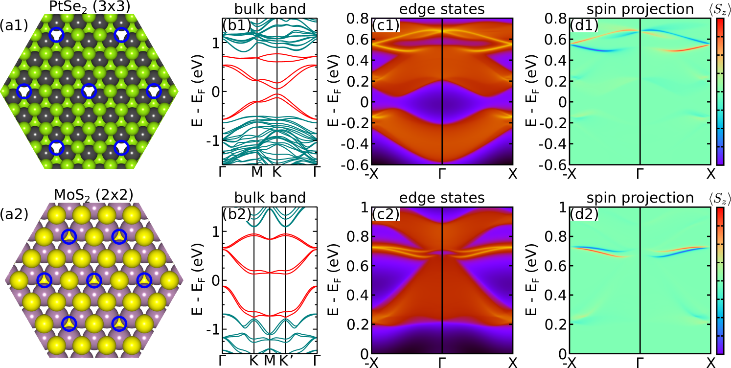
The topological phase in the PtSe2 vacancy system is quite robust, allowing experimental observation. Particularly, for the vacant hexagonal cell vac/cm2 (PtSe1.89) the topological SOC energy gap at is meV. Such values are higher than most predicted quantum spin Hall systems 24, and as we will show below, this guaranteed for a ribbon of only nm to already present the characteristic topological edge states. To highlight the topological phase we have constructed a semi-infinite system and characterize the edge states, as shown in Figure 3. Here, we can observe the edge states appearing within the bulk energy at filing, Figure 3(c1), with the spin-texture of such edge states obeying the backscattering forbidden character, Figure 3(d1). S-vacancy formation is also achieved in MoS2 system 25, 26 up to vac/cm2 19. Here a similar vacancy-driven topological mechanism is observed [Figure 3(a2)-(d2)], however with a smaller topological gap of meV for vac/cm2, given the lower relativistic effect of the Mo atoms.
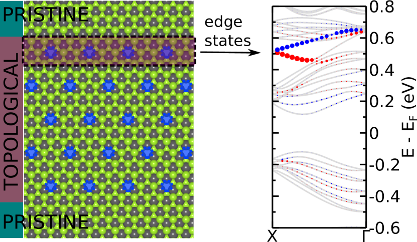
Taking advantage of the vacancy-controlled assembly by thermal treatment 12 in TMD, we have shown that the generation of topological states embedded on the semiconducting 2D systems can be constructed. Here we explicit construct the interface between pristine PtSe2 and a Se vacant region within DFT calculations [Figure 4]. We took a nanoribbon with a non-trivial region (vacant region) of nm separated from its periodic images by a trivial region, pristine PtSe2. The projected edge states’ contribution to the band structure (circles in the Figure 4 band) further confirms the characteristic spin-polarized states arising at the interface.
In conclusion, we report on the topological phase driven by vacancies on transition metal dichalcogenides. We show that the mediated interaction between the vacancies, together with the host SOC, leads to non-trivial states neatly lying on the semiconductor host energy gap. As a case of study, we characterize by ab initio approach the topological states in PtSe2, showing also the emergence on MoS2. In the former a topological gap of meV is among the highest predicted so far. A model enlightening the vacancy density dependence of the topological transition was obtained, which was shown to be useful in the prediction of the vacancy threshold for the topological phase. The proposed mechanism of vacancy-driven topology, allied with recent developments on autonomous control of atoms/vacancies on surfaces could allow an imprint of topological circuits in 2D systems in future device design.
Computational Approach
Density functional theory calculations were performed within the Vienna Ab initio Simulation package 27, with the PBE exchange-correlation term 28, a eV plane-wave base cutoff. The electron-ion interaction is considered within the projected augmented wave method 29, with all atoms relaxed until forces were lower than eV/Å. The special k-point of the 2D Brillouin zone was taken as Monkhorst-Pack grid for the cell and the same k-point density was used for the other cells. The relativistic SOC effect was considered in all calculations. The invariant was calculated by the Wannier base extraction for the vacancy states within the wannier90 package 30.
The authors acknowledge financial support from the Brazilian agencies FAPESP (grants 19/20857-0 and 17/02317-2), INCT-Nanomateriais de Carbono,, and Laboratório Nacional de Computação Científica for computer time.
References
- Corbett and Watkins 1965 Corbett, J. W.; Watkins, G. D. Production of Divacancies and Vacancies by Electron Irradiation of Silicon. Phys. Rev. 1965, 138, A555–A560
- Jiang et al. 2019 Jiang, J.; Xu, T.; Lu, J.; Sun, L.; Ni, Z. Defect Engineering in 2D Materials: Precise Manipulation and Improved Functionalities. Research 2019, 2019, 4641739
- Li et al. 2016 Li, G.; Zhang, D.; Qiao, Q.; Yu, Y.; Peterson, D.; Zafar, A.; Kumar, R.; Curtarolo, S.; Hunte, F.; Shannon, S.; Zhu, Y.; Yang, W.; Cao, L. All The Catalytic Active Sites of MoS2 for Hydrogen Evolution. Journal of the American Chemical Society 2016, 138, 16632–16638
- Park et al. 2004 Park, S. J.; Yeom, H. W.; Min, S. H.; Park, D. H.; Lyo, I. W. Direct Evidence of the Charge Ordered Phase Transition of Indium Nanowires on Si(111). Phys. Rev. Lett. 2004, 93, 106402
- Cai et al. 2015 Cai, L.; He, J.; Liu, Q.; Yao, T.; Chen, L.; Yan, W.; Hu, F.; Jiang, Y.; Zhao, Y.; Hu, T.; Sun, Z.; Wei, S. Vacancy-Induced Ferromagnetism of MoS2 Nanosheets. Journal of the American Chemical Society 2015, 137, 2622–2627
- Bragaglia et al. 2016 Bragaglia, V.; Arciprete, F.; Zhang, W.; Mio, A. M.; Zallo, E.; Perumal, K.; Giussani, A.; Cecchi, S.; Boschker, J. E.; Riechert, H.; Privitera, S.; Rimini, E.; Mazzarello, R.; Calarco, R. Metal-Insulator Transition Driven by Vacancy Ordering in GeSbTe Phase Change Materials. Scientific Reports 2016, 6, 23843
- Wang et al. 2019 Wang, Z.; Zhou, T.; Jiang, T.; Sun, H.; Zang, Y.; Gong, Y.; Zhang, J.; Tong, M.; Xie, X.; Liu, Q.; Chen, C.; He, K.; Xue, Q.-K. Dimensional Crossover and Topological Nature of the Thin Films of a Three-Dimensional Topological Insulator by Band Gap Engineering. Nano Letters 2019, 19, 4627–4633
- Li et al. 2009 Li, J.; Chu, R.-L.; Jain, J. K.; Shen, S.-Q. Topological Anderson Insulator. Phys. Rev. Lett. 2009, 102, 136806
- Groth et al. 2009 Groth, C. W.; Wimmer, M.; Akhmerov, A. R.; Tworzydło, J.; Beenakker, C. W. J. Theory of the Topological Anderson Insulator. Phys. Rev. Lett. 2009, 103, 196805
- Absor et al. 2017 Absor, M. A. U.; Santoso, I.; Harsojo,; Abraha, K.; Ishii, F.; Saito, M. Defect-induced large spin-orbit splitting in monolayer PtSe2. Phys. Rev. B 2017, 96, 115128
- Komsa et al. 2012 Komsa, H.-P.; Kotakoski, J.; Kurasch, S.; Lehtinen, O.; Kaiser, U.; Krasheninnikov, A. V. Two-Dimensional Transition Metal Dichalcogenides under Electron Irradiation: Defect Production and Doping. Phys. Rev. Lett. 2012, 109, 035503
- Lin et al. 2017 Lin, X. et al. Intrinsically patterned two-dimensional materials for selective adsorption of molecules and nanoclusters. Nature Materials 2017, 16, 717–721
- Gao et al. 2017 Gao, J.; Cheng, Y.; Tian, T.; Hu, X.; Zeng, K.; Zhang, G.; Zhang, Y.-W. Structure, Stability, and Kinetics of Vacancy Defects in Monolayer PtSe2: A First-Principles Study. ACS Omega 2017, 2, 8640–8648
- Pavliček et al. 2017 Pavliček, N.; Mistry, A.; Majzik, Z.; Moll, N.; Meyer, G.; Fox, D. J.; Gross, L. Synthesis and characterization of triangulene. Nature Nanotechnology 2017, 12, 308–311
- Slot et al. 2017 Slot, M. R.; Gardenier, T. S.; Jacobse, P. H.; van Miert, G. C. P.; Kempkes, S. N.; Zevenhuizen, S. J. M.; Smith, C. M.; Vanmaekelbergh, D.; Swart, I. Experimental realization and characterization of an electronic Lieb lattice. Nature Physics 2017, 13, 672–676
- Crasto de Lima and Miwa 2020 Crasto de Lima, F.; Miwa, R. H. Engineering Metal-spxy Dirac Bands on the Oxidized SiC Surface. Nano Letters 2020, 20, 3956–3962
- Nguyen et al. 2018 Nguyen, G. D.; Liang, L.; Zou, Q.; Fu, M.; Oyedele, A. D.; Sumpter, B. G.; Liu, Z.; Gai, Z.; Xiao, K.; Li, A.-P. 3D Imaging and Manipulation of Subsurface Selenium Vacancies in PdSe2. Phys. Rev. Lett. 2018, 121, 086101
- Qiu et al. 2013 Qiu, H.; Xu, T.; Wang, Z.; Ren, W.; Nan, H.; Ni, Z.; Chen, Q.; Yuan, S.; Miao, F.; Song, F.; Long, G.; Shi, Y.; Sun, L.; Wang, J.; Wang, X. Hopping transport through defect-induced localized states in molybdenum disulphide. Nature Communications 2013, 4, 2642
- Li et al. 2016 Li, H.; Tsai, C.; Koh, A. L.; Cai, L.; Contryman, A. W.; Fragapane, A. H.; Zhao, J.; Han, H. S.; Manoharan, H. C.; Abild-Pedersen, F.; Nørskov, J. K.; Zheng, X. Activating and optimizing MoS2 basal planes for hydrogen evolution through the formation of strained sulphur vacancies. Nature Materials 2016, 15, 48–53
- Liang et al. 2020 Liang, S.-J.; Cheng, B.; Cui, X.; Miao, F. Van der Waals Heterostructures for High-Performance Device Applications: Challenges and Opportunities. Advanced Materials 2020, 32, 1903800
- Focassio et al. 2021 Focassio, B.; Schleder, G. R.; Costa, M.; Fazzio, A.; Lewenkopf, C. Structural and electronic properties of realistic two-dimensional amorphous topological insulators. 2D Materials 2021, 8, 025032
- Pezo et al. 2021 Pezo, A.; Focassio, B.; Schleder, G. R.; Costa, M.; Lewenkopf, C.; Fazzio, A. Disorder effects of vacancies on the electronic transport properties of realistic topological insulator nanoribbons: The case of bismuthene. Phys. Rev. Materials 2021, 5, 014204
- de Lima et al. 2017 de Lima, F. C.; Ferreira, G. J.; Miwa, R. H. Tuning the topological states in metal-organic bilayers. Phys. Rev. B 2017, 96, 115426
- Marrazzo et al. 2019 Marrazzo, A.; Gibertini, M.; Campi, D.; Mounet, N.; Marzari, N. Relative Abundance of Z2 Topological Order in Exfoliable Two-Dimensional Insulators. Nano Letters 2019, 19, 8431–8440
- Hong et al. 2015 Hong, J. et al. Exploring atomic defects in molybdenum disulphide monolayers. Nature Communications 2015, 6, 6293
- Lu et al. 2014 Lu, C.-P.; Li, G.; Mao, J.; Wang, L.-M.; Andrei, E. Y. Bandgap, Mid-Gap States, and Gating Effects in MoS2. Nano Letters 2014, 14, 4628–4633
- Kresse and Furthmüller 1996 Kresse, G.; Furthmüller, J. Efficiency of ab-initio total energy calculations for metals and semiconductors using a plane-wave basis set. Computational Materials Science 1996, 6, 15–50
- Perdew et al. 1996 Perdew, J. P.; Burke, K.; Ernzerhof, M. Generalized Gradient Approximation Made Simple. Phys. Rev. Lett. 1996, 77, 3865–3868
- Blöchl 1994 Blöchl, P. E. Projector augmented-wave method. Phys. Rev. B 1994, 50, 17953–17979
- Pizzi et al. 2020 Pizzi, G. et al. Wannier90 as a community code: new features and applications. Journal of Physics: Condensed Matter 2020, 32, 165902