Enhancing the hybridization of plasmons in graphene with 2D superconductor collective modes
Abstract
We explore ways in which the close proximity between graphene sheets and monolayers of 2D superconductors can lead to hybridization between their collective excitations. We consider heterostructures formed by combinations of graphene sheets and 2D superconductor monolayers. The broad range of energies in which the graphene plasmon can exist, together with its tunability, makes such heterostrucutres promising platforms for probing the many-body physics of superconductors. We show that the hybridization between the graphene plasmon and the Bardasis-Schrieffer mode of a 2D superconductor results in clear signatures on the near-field reflection coefficient of the heterostructure, which in principle can be observed in scanning near-field microscopy experiments.
1 Introduction
Within the broad class of quantum two-dimensional (2D) materials, superconductors are arguably the most challenging, both from the theoretical and the experimental perspectives. On the other hand, their complex behaviour is teeming with possibilities, from unveiling new physics to providing the basis for disruptive technologies.
As with any other material, elementary excitations can provide insight about the fundamental physics of 2D superconductors. The strongly correlated nature of superconductors endows them with several collective modes, each carrying complementary pieces of information about the superconducting state. For instance, the Higgs mode, associated with oscillations of the amplitude of the superconducting order parameter, has energy dispersion [1, 2]
| (1) |
to leading order in the wave vector . Here, is the superconducting gap and is the Fermi velocity and is the dimensionality of the superconductor. Since its energy range lies close to and above the single particle excitation edge, the Higgs mode is damped. Moreover, its coupling to far-field electromagnetic radiation is rather weak [2], being suppressed by the small factor . Back in 1961, Bardasis and Schrieffer proposed [3] the existence of exciton-like collective modes in superconductors. Their eponymous excitation is a bound quasiparticle pair, and has a dispersion relation very similar to that of the Higgs mode. Its exciton-like character, however, implies its energy lies deep within the superconducting gap, making them long-lived excitations. They arise whenever the effective attractive electron-electron interaction, responsible for the pairing instability, has competing angular momentum components. It has been noted in the recent literature that characterization of the Bardasis-Schrieffer mode can help shed light on the nature of unconventional superconductivity, especially in Fe-based superconductors [4, 5].
From the recently synthesized 2D superconductors, one of the most promising and intriguing is FeSe, due to the record-high critical temperatures achieved for monolayers [6, 7]. Despite all the activity this system has attracted, the microscopic mechanisms by which is dramatically enhanced from the modest bulk value of K to K or even K [8] remain largely unknown [9].
It has been shown recently that combining graphene with superconductors in heterostructures can lead to fruitful interplay between their collective modes [10, 11, 12]. For instance, hybridization with graphene plasmons can enhance the visibility of the superconductor’s collective modes in optical experiments. By carefully designing the geometry of the heterostructure, several features of its electromagnetic response can be fine-tuned. Moreover, the incorporation of graphene provides a very convenient “handle” to modify the behavior of the heterostructure during operation, namely its doping level.
In this paper we study the near-field electromagnetic response of planar heterostructures combining monolayers of a 2D superconductor and graphene. We considered three kinds of heterostructures (shown schematically in figure 1): graphene-SC bilayers, graphene-SC-graphene sandwiches and SC-graphene-SC sandwiches. In all of them, a uniaxial dielectric (such as hexagonal boron nitride) is assumed as spacer between graphene and superconductor monolayers or between two superconductor monolayers. We calculate the heterostructure’s reflection coefficient associated with the incidence of -polarized waves by solving Maxwell’s equations subject to appropriate boundary conditions. The optical properties of hBN are incorporated into the calculations through its relative permittivity tensor, . Given the two-dimensional character of both graphene and the 2DSC, their properties only enter the calculations through BC. We model both graphene and the 2DSC by their non-local optical conductivity tensors [13, 14, 2]. For the superconductor we consider contributions coming from the Higgs mode and the Bardasis-Schrieffer mode [2]. As noted above, their features are directly tied to parameters that characterize the superconducting state, such as the superconducting gap and its symmetry, which makes them valuable probes into the nature of unconventional superconductivity. Moreover, their small dispersion in energy makes them perfect candidates for hybridizing with graphene plasmons [12]. The parameters that characterize FeSe were taken from reference [7]. There, through a multi-step annealing procedure, it was possible to change the carrier density from to electrons per Fe atom. They observe a pure superconducting phase for electrons per Fe atom.
Our results show a strong hybridization between the Bardasis-Schrieffer mode and the graphene plasmon, specially in the Gr-SC-Gr geometry. All geometries allow for tuning the optical response by changing either the heterostructure geometry (the thickness of the hBN spacer layers) or graphene’s doping level. The SC-Gr-SC geometry displays long-lived hybrid modes, which can be relevant for future applications. Moreover, we show that the hybridized modes impart their signature to the Purcell factor, which can be probed in scanning near-field optical microscopy (SNOM) experiments [15].
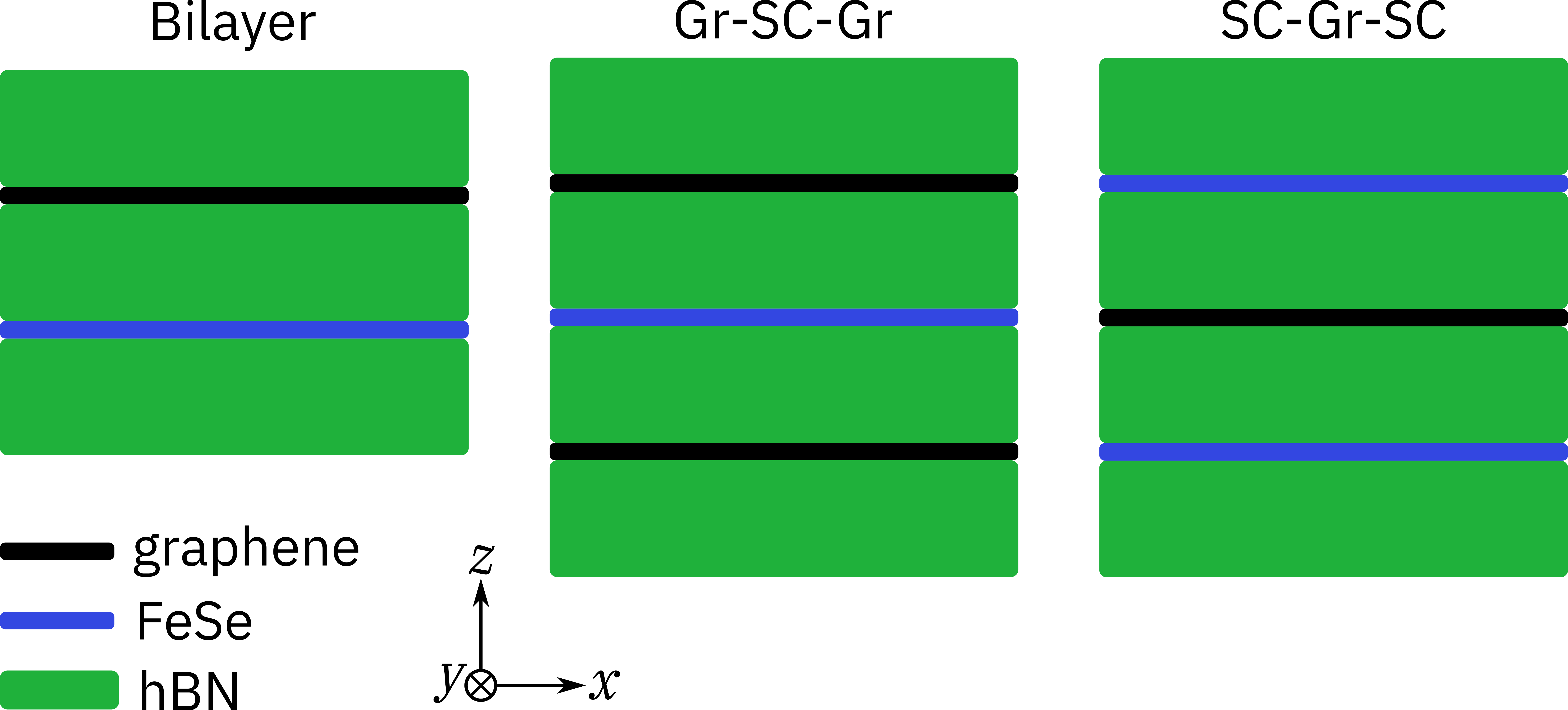
2 Bilayers
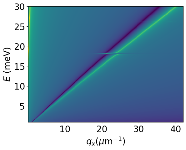
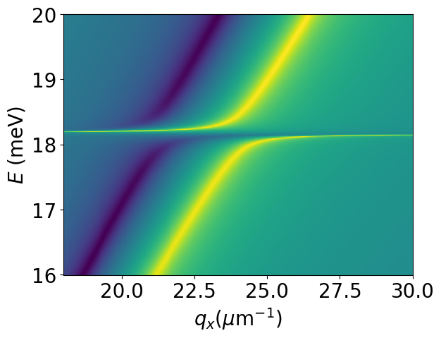
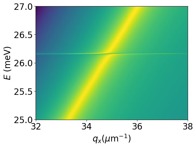
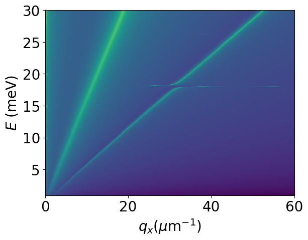
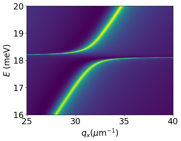
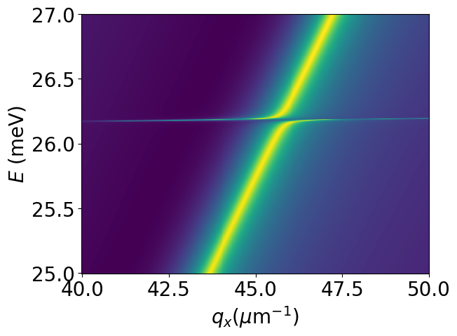
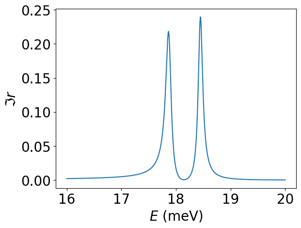
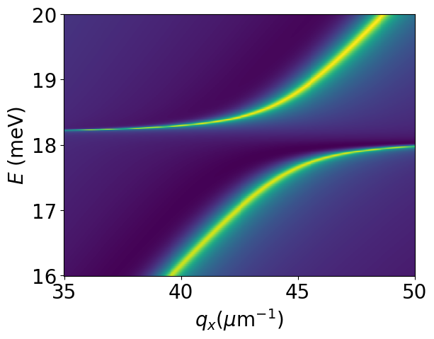
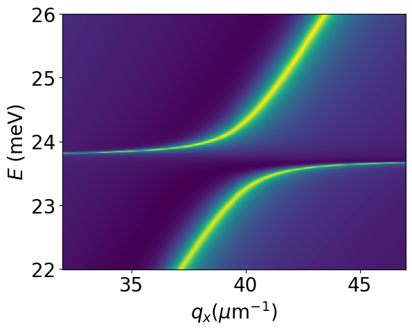
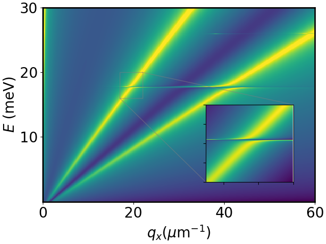
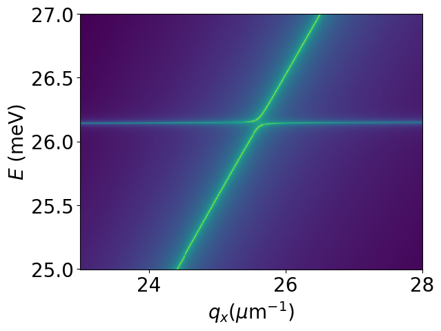
Here we consider the simplest heterostructure containing one graphene sheet and one monolayer of FeSe, separated by a thin layer of the insulator hBN of thickness . We calculate the frequency and wave vector dependent reflection coefficient to look for signatures of the FeSe collective modes. In fig. 2 we show the spectrum of electromagnetic waves as revealed by the imaginary part of the reflection coefficient for -polarized waves, . By zooming into the spectral region where the SC collective modes live we can get a clear picture of their hybridization with the graphene plasmon. It is known that the coupling of the Bardasis-Schrieffer mode with the electromagnetic field is stronger than the corresponding Higgs’ coupling by a factor of [2]. This is reflected by the size of the splitting between branches around the respective anticrossings, seen in fig. 2b and c. In the case of the Higgs mode, the tiny splitting between branches (eV) makes it harder to observe it than the Bardasis-Schrieffer mode.
3 Planar cavities
Here we consider two kinds of planar cavities: i) FeSe sandwiched between two graphene sheets, ii) or a graphene sheet is sandwiched between two monolayers of FeSe. Again, the separation between graphene and FeSe is achieved by a thin layer of hBN.
3.1 Gr - FeSe - Gr
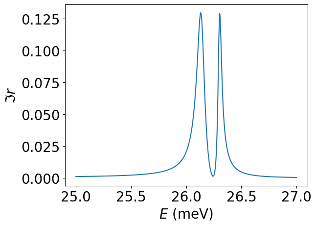
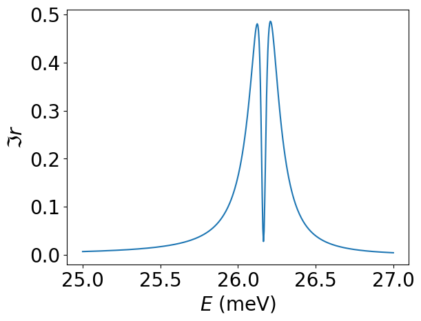
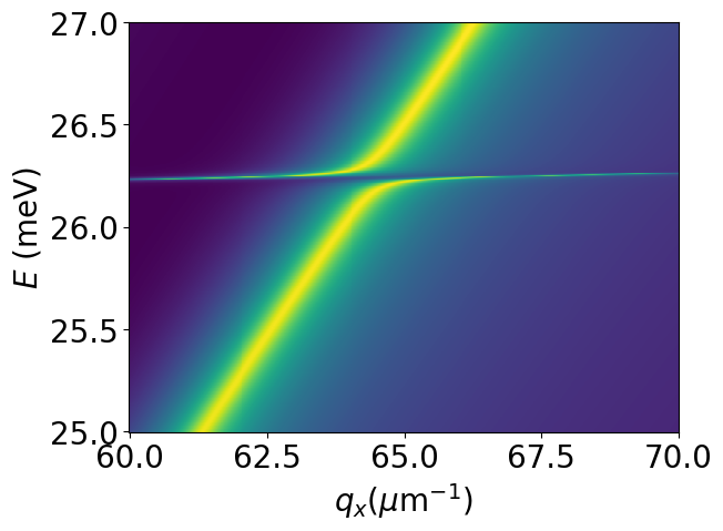
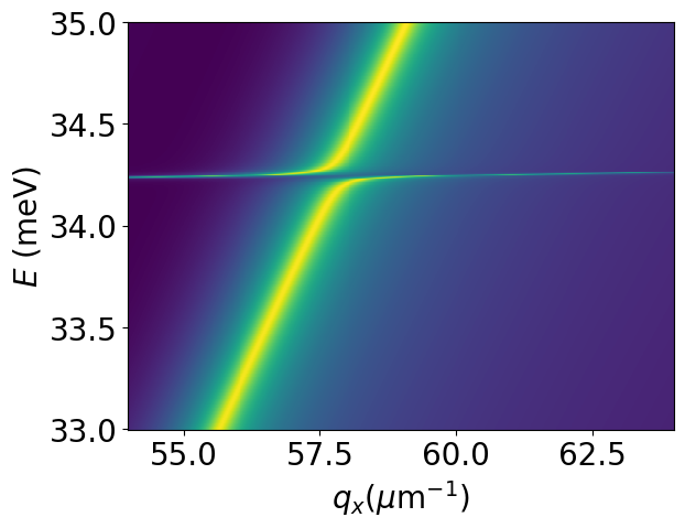
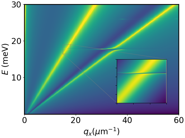
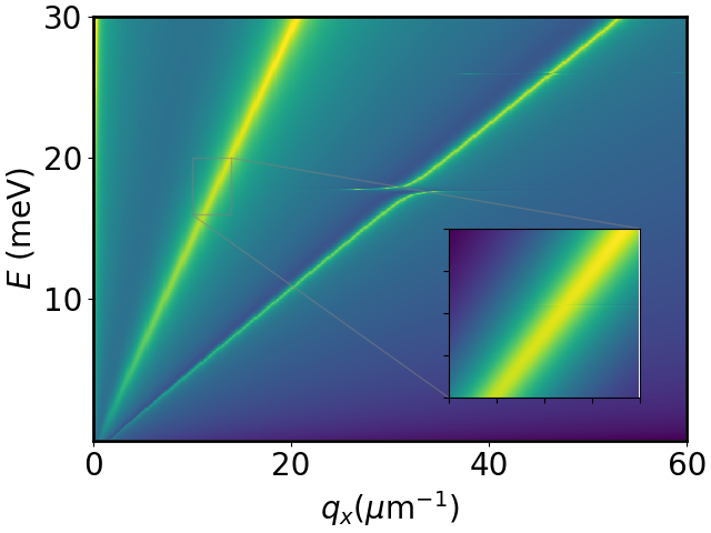
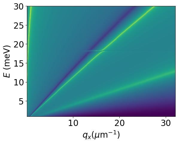
When compared with the results for the bilayer geometry, we see an increase in the splitting between the branches around the anticrossing, both for the Bardasis-Schrieffer and for the Higgs mode (fig. 3). Also noticeable is a reduction of the linewidth of both branches (better seen in an energy cut along a fixed wave vector, as in fig 4. This means that the sandwich geometry produces longer-lived hybrid modes than the simpler bilayer geometry, which could be important for applications. Also relevant for potential applications is the fact that the features of the hybrid modes can be controlled electrostatically via graphene’s doping level. Changing the thickness of the insulator layers provides one way to control the features of the hybrid modes, as seen in fig. 6.
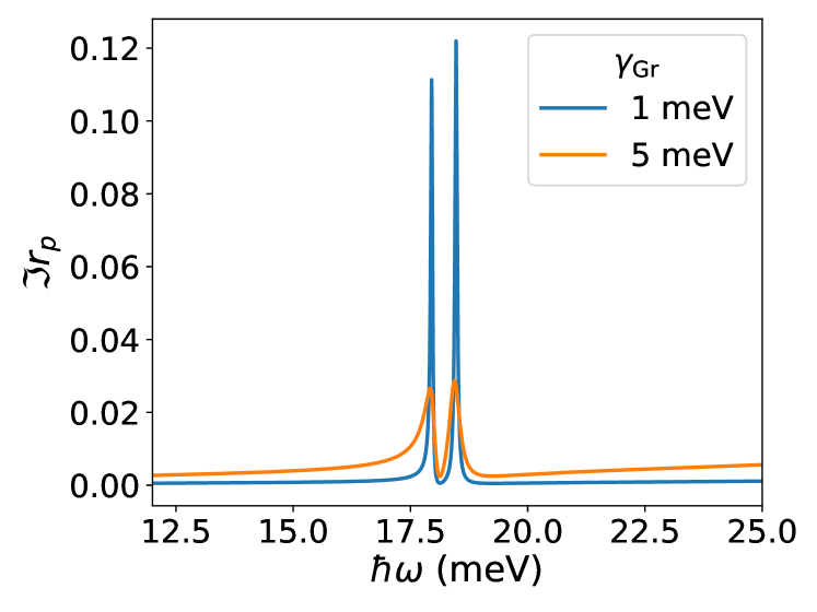
In order to enhance the visibility of the features associated with the hybridized modes, we have adopted a fairly small relaxation rate for graphene ( meV). Nevertheless, the hybrid modes can still be clearly seen at higher relaxation rates, as shown in figure 5. In fact, those linewidths are considerably smaller than . For meV the linewidths are meV, and for meV we find linewidths meV. This means that observation of the hybrid graphene plasmon – Bardasis-Schrieffer mode is possible with existing graphene preparation techniques.
We note that, in this sandwich geometry, only the anti-symmetric graphene plasmon (the lower energy branch) couples to the superconductor. This is related to the fact that the electric field at the position of the SC sheet (right in the middle of the sandwich) is zero for the symmetric mode. To allow both branches to couple to the SC we must break the symmetry, either by placing the SC sheet off center, or by applying different gate voltages to the two graphene sheets. In figure 8 we show the results for the latter case. It is interesting to note that Fermi energy imbalance between the graphene sheets must be relatively large to make the coupling of the high energy mode to the SC visible.
3.2 FeSe - Gr - FeSe
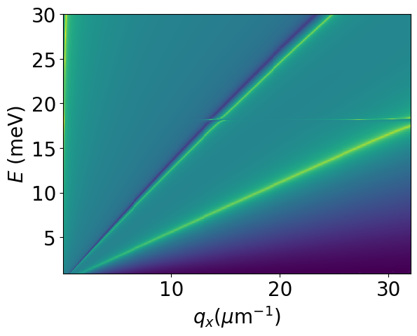
Superconducting waveguides have been discussed in the literature [16] as promising building blocks for future plasmonic technologies, due to the intrinsic low-loss associated with the dynamics of the Cooper-pair condensate. In the original proposal [16], the cavity geometry serves the purpose of overcoming the problem of weak confinement of the plasmon to the surface of bulk superconductors. In the context of 2D superconductors, the same geometry can be exploited to promote the coupling of the (small dispersion) Bardasis-Schrieffer and Higgs modes to the anti-symmetric Cooper-pair plasmon, as shown in figure 9. Of course, the anti-symmetric mode itself can be used as a resource for plasmonic technologies, as suggested in the literature [16]. The features of the anti-symmetric mode can be tuned in the manufacturing process, by adjusting the distance between the SC monolayers and/or changing the insulating spacer material. It may be desirable, however, to have the ability to control those features on-the-fly. Incorporating a graphene sheet into the device may provide such a control. Due to the anti-symmetric nature of the mode, however, it couples weakly to objects that are placed close to the middle point between the two FeSe monolayers. Thus, to obtain control over the dispersion relation of the anti-symmetric mode, the graphene sheet must be placed much closer to one of the FeSe monolayers than to the other.
For the sake of comparison, we start by showing the results for a cavity formed by two FeSe monolayers separated by a 12 nm thick slab of hBN. The anti-crossings between the Ba-Sh anti-symmetric plasmon mode is clearly visible. To notice the anti-crossing in the case of the Higgs mode it is necessary to zoom in, as shown in fig. 9.
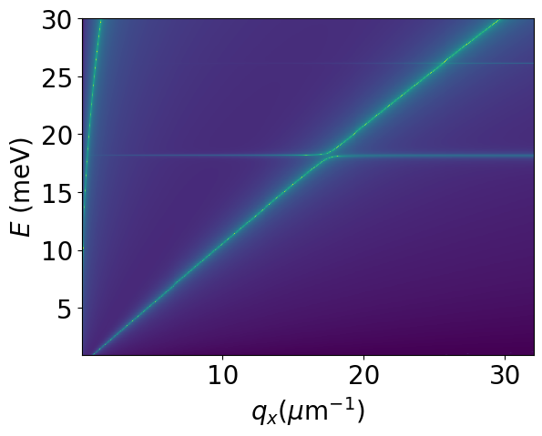
By sandwiching one graphene sheet between the two FeSe monolayers, we add the possibility to tune certain features of the excitation spectrum of the heterostructure. For instance, by changing the graphene sheet’s doping level it is possible to control the dispersion relation of the anti-symmetric plasmon branch associated with the cooper-pairs, as seen in fig. 10.
4 Purcell factor
Direct observation of the hybrid graphene plasmon-superconductor is difficult because of the mismatch between the wave vector of light and that of the hybrid excitation. One way to partially circumvent this difficulty is to consider the effects of the hybrid modes on a nearby quantum emitter [13, 17, 18, 19]. Its rate of spontaneous emission is modified by the presence of the heterostructure, and this modification carries information about the reflection coefficients of the heterostructure. This is encoded in the ratio between the electromagnetic local density of states (LDOS) in the presence of the heterostructure and the LDOS of free space, given by [13]
| (2) |
where , with and is the distance between the emitter and the topmost hBN layer. This ratio is known as the Purcell factor [20, 21, 22], and can be very large when the emitter is placed close to surfaces that support localized electromagnetic modes.
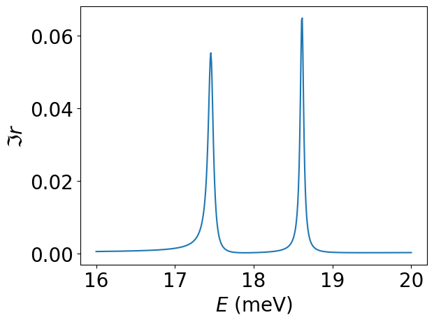
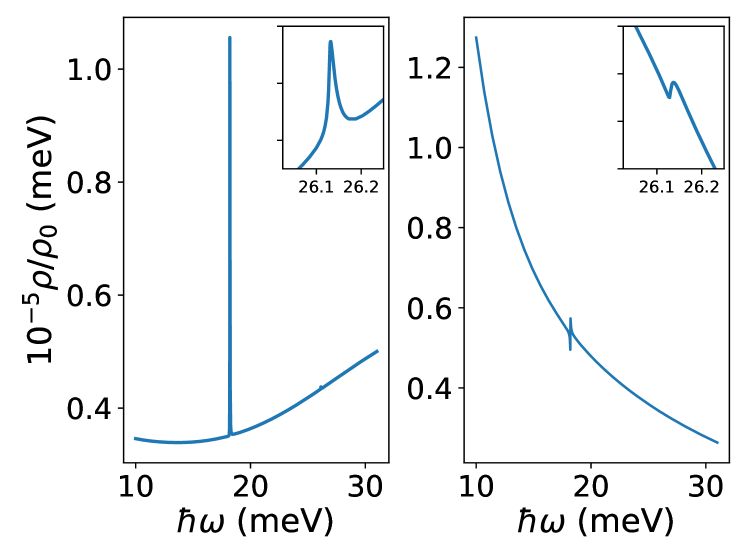
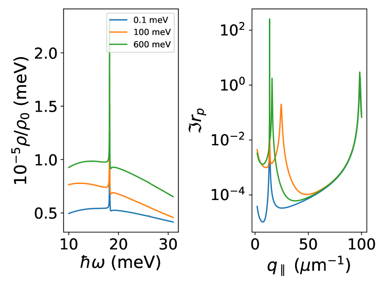
In figure 11 we show the Purcell factor for a Gr-FeSe-Gr heterostructure as a function of the emitter frequency. The emitter has been placed at a distance nm from the surface, corresponding to an effective wave vector of . In the limit of vanishing graphene doping ( meV, left panel) the LDOS displays a clear peak at the frequency of the Bardasis-Schrieffer mode. It also has a much smaller peak at the frequency of the Higgs mode, as expected due to the weakness of the coupling between the Higgs mode and the electromagnetic field [2]. In the right panel we show the Purcell factor for meV. Both the lineshape and the size of the features (relative to the background) are strongly influenced by the charge density in the graphene sheets. These changes reflect the fact that the hybridization between the SC modes and the graphene plasmon transfers spectral weight from a very narrow frequency range (corresponding to the very weakly dispersing SC modes) to the hybrid excitations, both of which have significant dispersion.
The Purcell factor for the SC-Gr-SC heterostructure displays a much sharper feature when compared to the Gr-SC-Gr structure, as seen in figure 12. The Purcell factor in this case is dominated by the very sharp peak in at small wave vector, associated with hybridization between the anti-symmetric Cooper pair plasmon and the Bardasis-Schrieffer mode (see the right panel of figure 12). The hybridization between the graphene plasmon and the Bardasis-Schrieffer mode occurs at a larger wave vector (close to 100 m-1). Thus, as we will show below, its contribution is much attenuated due to the filtering property of the Purcell factor.
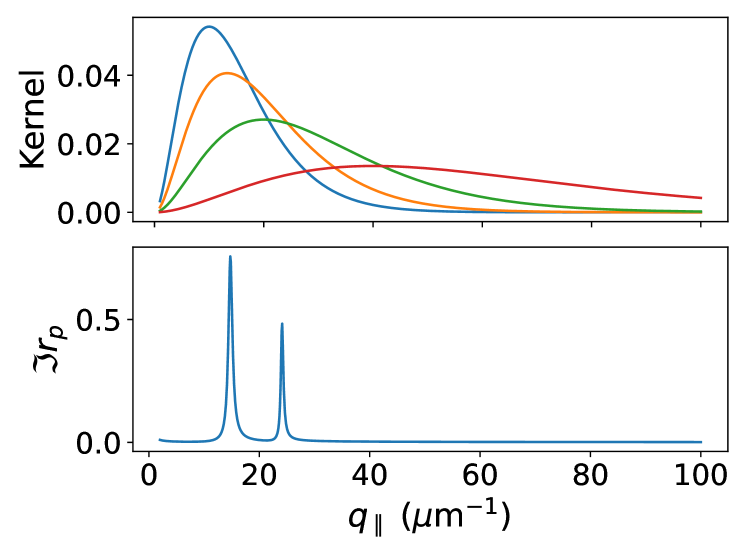
We now comment briefly on the relationship between features in the near-field reflection coefficient and in the Purcell factor. Notice that the kernel
| (3) |
acts as a filter for the reflection coefficient . In particular, for , and
| (4) |
This function has a maximum close to , but the width of this peak depends strongly on both and . To illustrate the filtering property of the kernel we fix meV, which is close to the energy of the Bardasis-Schrieffer mode, and plot
| (5) |
as a function of for a few values of . The normalization factor
| (6) |
is introduced to facilitate the visual comparison between the curves with different values of . The results are shown in figure 13. It is readily noticeable that the filtering function is much broader than the typical features of the reflection coefficient. This constrains the degree of detail with which features in can be resolved, depending on the wave vector around which they appear. This is important to keep in mind when choosing the placement of the LDOS probe relative to the system.
5 Concluding remarks
We have shown that heterostructures of simple geometry, formed by graphene and 2D superconductors separated by a few nanometers, display clear signatures of hybridization between their respective collective modes. The planar cavity geometry Gr-SC-Gr promotes a strong enhancement of the hybridization. It also provides tunability, either through adjustment of geometric parameters or on-the-fly modification of graphene’s doping levels. On the other hand, in the SC-Gr-SC cavity the hybridization is typically weak, but still the graphene doping level can be used to control the features of the SC collective modes. Our results show that graphene-2D superconductor heterostructures are promising platforms for probing the fundamental properties of 2D superconductors and for future applications.
References
References
- [1] Littlewood P B and Varma C M 1982 Phys. Rev. B 26(9) 4883–4893 URL https://link.aps.org/doi/10.1103/PhysRevB.26.4883
- [2] Sun Z, Fogler M M, Basov D N and Millis A J 2020 Phys. Rev. Research 2(2) 023413 URL https://link.aps.org/doi/10.1103/PhysRevResearch.2.023413
- [3] Bardasis A and Schrieffer J R 1961 Phys. Rev. 121(4) 1050–1062 URL https://link.aps.org/doi/10.1103/PhysRev.121.1050
- [4] Müller M A, Volkov P A, Paul I and Eremin I M 2021 Phys. Rev. B 103(2) 024519 URL https://link.aps.org/doi/10.1103/PhysRevB.103.024519
- [5] Maiti S and Hirschfeld P J 2015 Phys. Rev. B 92(9) 094506 URL https://link.aps.org/doi/10.1103/PhysRevB.92.094506
- [6] Wang Q Y, Li Z, Zhang W H, Zhang Z C, Zhang J S, Li W, Ding H, Ou Y B, Deng P, Chang K, Wen J, Song C L, He K, Jia J F, Ji S H, Wang Y Y, Wang L L, Chen X, Ma X C and Xue Q K 2012 Chinese Physics Letters 29 037402 URL https://doi.org/10.1088/0256-307x/29/3/037402
- [7] He S, He J, Zhang W, Zhao L, Liu D, Liu X, Mou D, Ou Y B, Wang Q Y, Li Z, Wang L, Peng Y, Liu Y, Chen C, Yu L, Liu G, Dong X, Zhang J, Chen C, Xu Z, Chen X, Ma X, Xue Q and Zhou X J 2013 Nature Materials 12 605–610 ISSN 1476-4660 URL https://doi.org/10.1038/nmat3648
- [8] Ge J F, Liu Z L, Liu C, Gao C L, Qian D, Xue Q K, Liu Y and Jia J F 2015 Nat Mater 14 285–289
- [9] Huang D and Hoffman J E 2017 Annual Review of Condensed Matter Physics 8 311–336 (Preprint https://doi.org/10.1146/annurev-conmatphys-031016-025242) URL https://doi.org/10.1146/annurev-conmatphys-031016-025242
- [10] Reserbat-Plantey A, Epstein I, Torre I, Costa A T, Gonçalves P A D, Mortensen N A, Polini M, Song J C W, Peres N M R and Koppens F H L 2021 ACS Photonics 8 85–101 (Preprint https://doi.org/10.1021/acsphotonics.0c01224) URL https://doi.org/10.1021/acsphotonics.0c01224
- [11] Berkowitz M E, Kim B S Y, Ni G, McLeod A S, Lo C F B, Sun Z, Gu G, Watanabe K, Taniguchi T, Millis A J, Hone J C, Fogler M M, Averitt R D and Basov D N 2021 Nano Letters 21 308–316 pMID: 33320013 (Preprint https://doi.org/10.1021/acs.nanolett.0c03684) URL https://doi.org/10.1021/acs.nanolett.0c03684
- [12] Costa A T, Gonçalves P A D, Basov D N, Koppens F H L, Mortensen N A and Peres N M R 2021 Proceedings of the National Academy of Sciences 118 ISSN 0027-8424 (Preprint https://www.pnas.org/content/118/4/e2012847118.full.pdf) URL https://www.pnas.org/content/118/4/e2012847118
- [13] Gonçalves P A D and Peres N M R 2016 An Introduction to Graphene Plasmonics 1st ed (Singapore: World Scientific) URL http://www.worldscientific.com/worldscibooks/10.1142/9948
- [14] Dias E J C, Iranzo D A, Gonçalves P A D, Hajati Y, Bludov Y V, Jauho A P, Mortensen N A, Koppens F H L and Peres N M R 2018 Phys. Rev. B 97(24) 245405 URL https://link.aps.org/doi/10.1103/PhysRevB.97.245405
- [15] Ni G X, McLeod A S, Sun Z, Wang L, Xiong L, Post K W, Sunku S S, Jiang B Y, Hone J, Dean C R, Fogler M M and Basov D N 2018 Nature 557 530–533 URL https://doi.org/10.1038/s41586-018-0136-9
- [16] Tsiatmas A, Fedotov V A, de Abajo F J G and Zheludev N I 2012 New Journal of Physics 14 115006 URL https://doi.org/10.1088/1367-2630/14/11/115006
- [17] Koppens F H L, Chang D E and García de Abajo F J 2011 Nano Lett. 11 3370–3377 ISSN 1530-6984 URL https://doi.org/10.1021/nl201771h
- [18] Schädler K G, Ciancico C, Pazzagli S, Lombardi P, Bachtold A, Toninelli C, Reserbat-Plantey A and Koppens F H L 2019 Nano Lett. 19 3789–3795 ISSN 1530-6984 URL https://doi.org/10.1021/acs.nanolett.9b00916
- [19] Kurman Y, Rivera N, Christensen T, Tsesses S, Orenstein M, Soljačić M, Joannopoulos J D and Kaminer I 2018 Nat. Photon. 12 423–429 ISSN 1749-4893 URL https://doi.org/10.1038/s41566-018-0176-6
- [20] Purcell E M 1946 Phys. Rev. 69 681 URL https://link.aps.org/doi/10.1103/PhysRev.69.674.2
- [21] Novotny L and Hecht B 2012 Principles of Nano-Optics 2nd ed (Cambridge University Press)
- [22] Gonçalves P A D 2020 Plasmonics and Light–Matter Interactions in Two-Dimensional Materials and in Metal Nanostructures: Classical and Quantum Considerations (Springer Nature) URL http://doi.org/10.1007/978-3-030-38291-9